

Page 1
AN3232
Application note
Mounting recommendations
for STAC
Introduction
RF power transistors are amongst the highest power density devices in the semiconductor
industry. It is crucial to the reliability and performance of such devices to consider
mechanical stress and thermal and electrical resistance within the application environment.
®
boltdown packages
The general purpose of this application note is to provide guidelines for mounting various
types of STAC
by soldering. Specific attention is paid to the STAC244B and STAC265B boltdown styles and
the STAC244F and STAC265F flangeless styles, which are used to encapsulate numerous
VDMOS and LDMOS technology products.
This application note is intended to provide mounting tips and design guidelines. For actual
data please refer to the relevant product datasheet.
STAC
is a registered trademarks of STMicroelectronics.
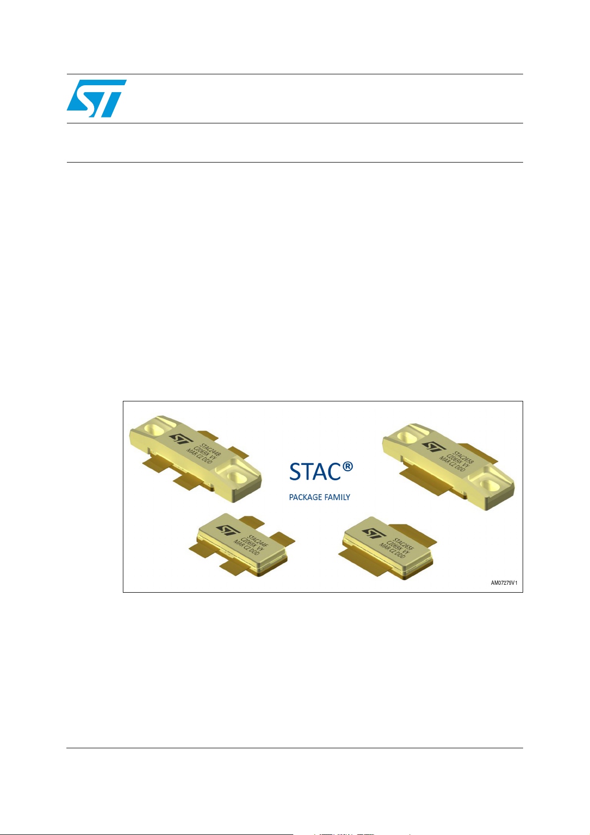
Figure 1. STAC boltdown packages
®
packages in amplifiers or application boards (PCB) by means of bolting or
August 2011 Doc ID 17594 Rev 3 1/26
www.st.com
Page 2

Contents AN3232
Contents
1 Epoxy sealed, non-hermetic RF power packages . . . . . . . . . . . . . . . . . 5
2 Exceptional thermal performance potential of the STAC package
concept . . . . . . . . . . . . . . . . . . . . . . . . . . . . . . . . . . . . . . . . . . . . . . . . . . . . 7
3 Heatsink selection . . . . . . . . . . . . . . . . . . . . . . . . . . . . . . . . . . . . . . . . . . . 9
4 Core preparation . . . . . . . . . . . . . . . . . . . . . . . . . . . . . . . . . . . . . . . . . . . 10
5 Mounting base surface conditions . . . . . . . . . . . . . . . . . . . . . . . . . . . . 11
6 Thermal interface material . . . . . . . . . . . . . . . . . . . . . . . . . . . . . . . . . . . 12
7 Seating plane . . . . . . . . . . . . . . . . . . . . . . . . . . . . . . . . . . . . . . . . . . . . . . 13
8 Printed circuit board (PCB) considerations . . . . . . . . . . . . . . . . . . . . . 15
9 Package attachment to core by means of boltdown method . . . . . . . 16
9.1 Required hardware . . . . . . . . . . . . . . . . . . . . . . . . . . . . . . . . . . . . . . . . . . 16
9.2 Considerations . . . . . . . . . . . . . . . . . . . . . . . . . . . . . . . . . . . . . . . . . . . . . 16
9.3 Procedure summary . . . . . . . . . . . . . . . . . . . . . . . . . . . . . . . . . . . . . . . . . 19
10 Package attachment to thermal base by means of soldering . . . . . . . 20
10.1 Hardware . . . . . . . . . . . . . . . . . . . . . . . . . . . . . . . . . . . . . . . . . . . . . . . . . 20
10.2 Solder reflow equipment and methods . . . . . . . . . . . . . . . . . . . . . . . . . . . 20
11 Electrical connection . . . . . . . . . . . . . . . . . . . . . . . . . . . . . . . . . . . . . . . 23
12 Conclusion . . . . . . . . . . . . . . . . . . . . . . . . . . . . . . . . . . . . . . . . . . . . . . . . 24
13 Revision history . . . . . . . . . . . . . . . . . . . . . . . . . . . . . . . . . . . . . . . . . . . 25
2/26 Doc ID 17594 Rev 3
Page 3

AN3232 List of tables
List of tables
Table 1. Preferred copper core thickness . . . . . . . . . . . . . . . . . . . . . . . . . . . . . . . . . . . . . . . . . . . . . . 9
Table 2. Surface conditions . . . . . . . . . . . . . . . . . . . . . . . . . . . . . . . . . . . . . . . . . . . . . . . . . . . . . . . 11
Table 3. Common TIMs . . . . . . . . . . . . . . . . . . . . . . . . . . . . . . . . . . . . . . . . . . . . . . . . . . . . . . . . . . 12
Table 4. Recommended screw torque . . . . . . . . . . . . . . . . . . . . . . . . . . . . . . . . . . . . . . . . . . . . . . . 18
Table 5. Pb-free process - package classification reflow temperatures . . . . . . . . . . . . . . . . . . . . . . 21
Table 6. Document revision history . . . . . . . . . . . . . . . . . . . . . . . . . . . . . . . . . . . . . . . . . . . . . . . . . 25
Doc ID 17594 Rev 3 3/26
Page 4

List of figures AN3232
List of figures
Figure 1. STAC boltdown packages . . . . . . . . . . . . . . . . . . . . . . . . . . . . . . . . . . . . . . . . . . . . . . . . . . 1
Figure 2. Drying times . . . . . . . . . . . . . . . . . . . . . . . . . . . . . . . . . . . . . . . . . . . . . . . . . . . . . . . . . . . . . 5
Figure 3. Infrared imaging of a STAC package . . . . . . . . . . . . . . . . . . . . . . . . . . . . . . . . . . . . . . . . . . 7
Figure 4. Pocket depth consideration (mm) . . . . . . . . . . . . . . . . . . . . . . . . . . . . . . . . . . . . . . . . . . . . 13
Figure 5. Lead bending . . . . . . . . . . . . . . . . . . . . . . . . . . . . . . . . . . . . . . . . . . . . . . . . . . . . . . . . . . . 13
Figure 6. Package cut and pads layout . . . . . . . . . . . . . . . . . . . . . . . . . . . . . . . . . . . . . . . . . . . . . . . 15
Figure 7. Ideal screw-center spacing . . . . . . . . . . . . . . . . . . . . . . . . . . . . . . . . . . . . . . . . . . . . . . . . . 17
Figure 8. First boltdown mounting steps . . . . . . . . . . . . . . . . . . . . . . . . . . . . . . . . . . . . . . . . . . . . . . 18
Figure 9. SEHO FDS “MAXIPOWER” reflow oven . . . . . . . . . . . . . . . . . . . . . . . . . . . . . . . . . . . . . . 20
Figure 10. Component level temperature profile . . . . . . . . . . . . . . . . . . . . . . . . . . . . . . . . . . . . . . . . . 21
4/26 Doc ID 17594 Rev 3
Page 5
AN3232 Epoxy sealed, non-hermetic RF power packages
1 Epoxy sealed, non-hermetic RF power packages
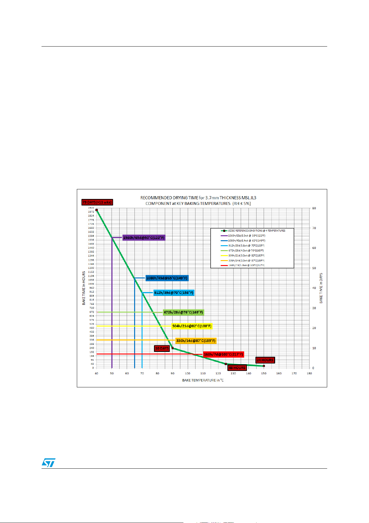
Epoxy sealed products, such as the STAC package family, should be received in an N2backfilled, vacuum-sealed ESD bag containing a desiccant. This decreases the possibility of
moisture uptake by the package materials during transit and long-term storage. STAC
packages carry a moisture sensitivity rating of 3 (MSL3), but have demonstrated capabilities
of up to MSL1.
Even with such shipping methods, it is advised to store epoxy sealed packages in the
original containers, or in a dry box, until required for soldering. When the environmental
history of devices is not well-known, such as after a prolonged storage period, it is a wellpracticed safety measure to bake non-hermetic packages for 24 hrs at 125 °C prior to
soldering operations. These conditions can be accelerated or lengthened as a function of
temperature, up to the limits imposed by shipping containers, by trays, or by device
maximum ratings. Refer to Figure 2 for recommended baking conditions.
Figure 2. Drying times
Under no circumstances should any epoxy-sealed package be treated as a hermetically
sealed package, due to the fact that such sealing materials are not impervious to moisture
ingress. However, it is important to point out that RF Power packages are typically
constructed using engineering ceramics and polymers which, on their own, demonstrate
high resistance to moisture penetration, such as the proprietary liquid crystal polymer
materials upon which STAC packages are realized.
Doc ID 17594 Rev 3 5/26
Page 6

Epoxy sealed, non-hermetic RF power packages AN3232
Power RF packages typically require a reliable, low thermal resistance attachment to a
heatsink. In this respect, nothing out-performs a direct attachment of the device flange, or
thermal base, to the heatsink by means of soldering. This can be accomplished using any of
the PbSn or Pb-free soldering methods used throughout the electronic industry. The final
soldering step may be preceded by a hot-solder dip of the package base and/or leads, as
required for situations that require attention to Au content of the solder joint. Alternatively,
the packages may be inserted into an amplifier using a pick-and-place methodology, so that
complete soldering is accomplished in a single reflow.
Some amplifier assemblies require a manual approach for device positioning on a PCB
while soldering bases to copper core heatsinks. In such manual operations STAC boltdown
style packages have the unique possibility of serving as a built-in clamp to accomplish both
tasks expeditiously. These manual efforts are rewarded by an extremely low thermal
resistance, achieved by an ultra-thin solder joint case-to-heatsink, referred to as the Rth
. At the same time, the need to allocate valuable amplifier real estate to specialized
HS
C-
clamping fixtures is eliminated.
The approaches to soldering RF transistors in amplifier housings are as numerous as the
quantity of RF package outlines. While the traditional demand for high levels of ruggedness
in RF devices assures an intrinsic high tolerance to a wide variety of assembly methods, the
high-stress nature of any soldering operation requires careful consideration. Users
ultimately assume responsibility for developing and qualifying their soldering processes, and
therefore it is strongly recommended to fully evaluate temperature profiles at all steps in the
soldering procedure to avoid excessive peak temperatures and ramp rates.
When amplifier assemblies require cleaning after soldering operations, the use of a nonreactive cleaning agent is recommended. All residue from reactive flux should be removed
according to the flux supplier's recommendations.
If a non-aqueous cleaning method is employed, it must be followed by cleaning with DI water
to remove all ionic contamination. It is recommended to periodically check the conductivity
of the DI rinse to insure that levels of ionic contamination are as low as possible. In cases
where heavy ionic contamination is present, multiple DI rinses in isolated baths should be
used. Proceed from the most to the least contaminated rinsing system to maximize cleaning
effectiveness.
In general it is recommended to minimize the use of flux, to use no-clean flux, or to adopt
fluxless soldering techniques. When there is doubt as to the behavior of residual flux or flux
levels, consider a two-step solder approach. Since the PCB and other components may
involve flux, an initial soldering step of the majority of non-critical components can be done,
followed by a thorough cleaning. The second solder step, with greatly reduced flux content,
can be planned for more critical components such as epoxy sealed RF transistors. An
added benefit of a two-step operation is that non-solder thermal interface materials (TIMs),
such as thermal compounds, are not influenced by aggressive flux cleaning.
Following DI rinsing operations, the entire assembly should be baked, as determined by
user experimentation, before power is applied. It is suggested to perform this drying at 125
°C for 24 hrs, if all components are rated for this condition. A longer bake time is
recommended at lower temperatures. Refer to Figure 2 for some suggestions.
OEM equipment operating conditions should be specified for operation only in a “noncondensating” environment. If there is a question of humidity in ambient conditions in power
cycling, a heating/drying cycle is recommended before power is applied.
6/26 Doc ID 17594 Rev 3
Page 7
AN3232 Exceptional thermal performance potential of the STAC package concept
2 Exceptional thermal performance potential of the
STAC package concept
RF Power transistors are made up of hundreds of thousands of heat generating cells,
organized in an ultra-compact geometry at the silicon chip level. The necessity to generate
RF power at ever-increasing frequencies leads directly to the shrinking of silicon geometries
to ever-smaller portions of electrical wavelength. The result is unprecedented power density,
unmatched by most devices in the semiconductor industry. Indeed, such a power density
approaches those frequently encountered in the realm of high-energy physics.
The highest priority of the power transistor package is efficient evacuation of the incredible
thermal flux from the active regions of semiconductor chips to the external environment.
Great advances made to improve packaging systems and materials have enhanced this
effect, including the use of high thermal conductivity materials, the reduction of thermal path
length, and the improvement of thermal interfaces by way of superior flatness coupled with
enhanced TIMs.
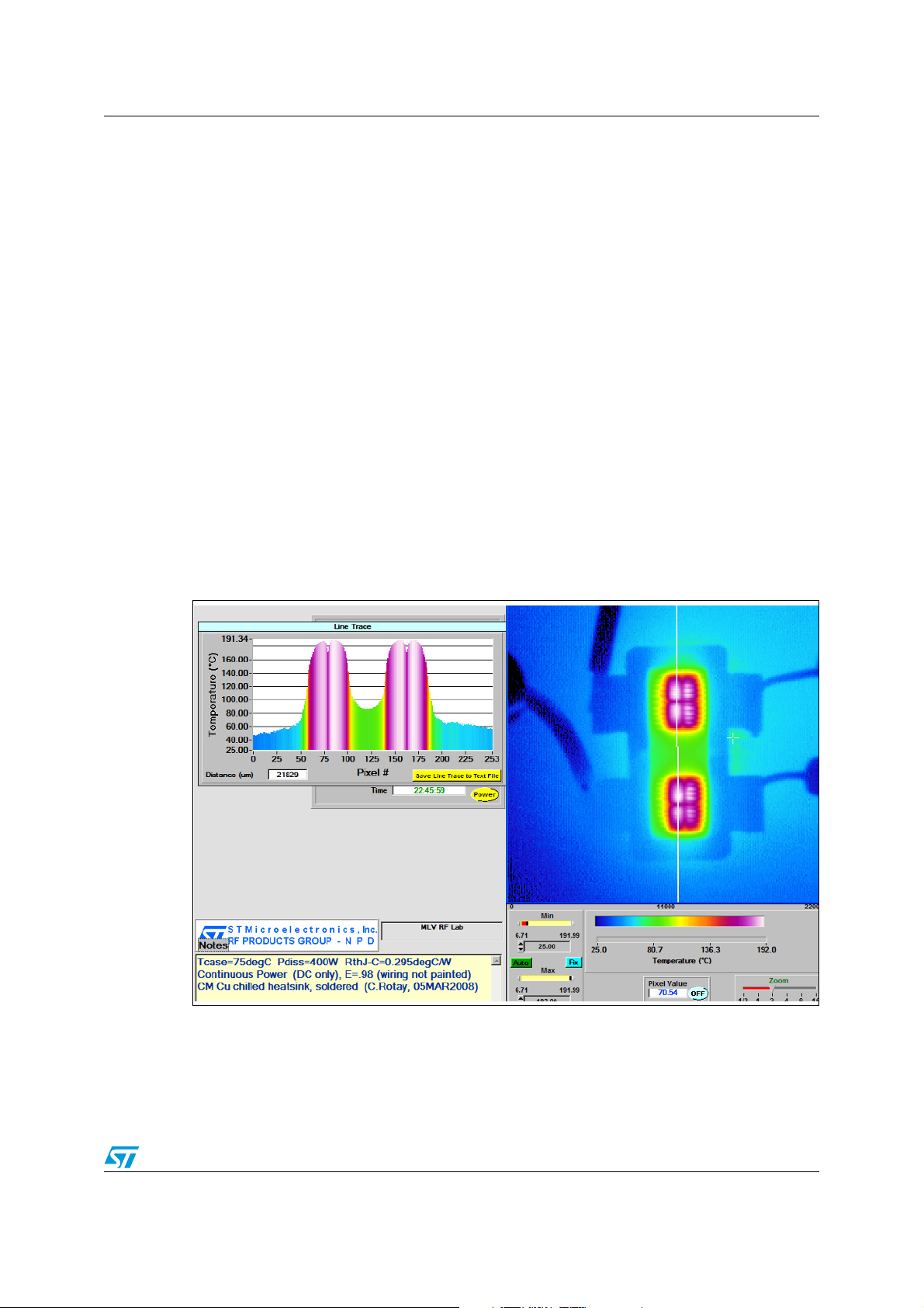
A demonstration of the high power density of one device in the STAC family is shown in
Figure 3 by way of infrared imaging. In this example, the junction temperature of the
semiconductor chips, dissipating a total of 400 W continuously, is maintained uniformly
below the maximum allowable temperature of 200 °C, while the case is elevated almost to
its maximum of 85 °C.
Figure 3. Infrared imaging of a STAC package
As is the case with many RF power devices, thermal resistance is dominated by the chips
themselves, as can be ascertained in Figure 3. In addition, the thermal conductivity of
silicon decreases with increasing temperature, therefore it is common practice to evaluate
power transistors near the maximum operating temperatures. Taking this into account, the
observed thermal resistance, or R
of approximately 0.30 °C/W for this STAC product, is
thJ-C
Doc ID 17594 Rev 3 7/26
Page 8

Exceptional thermal performance potential of the STAC package concept AN3232
approximately 30 % lower than it's ceramic package cousin, the ubiquitous GEMINI
package.
This situation affords amplifier designers extreme flexibility in terms of trade-offs between
power dissipated, output power, power density, and MTTF. For example, higher power can
be dissipated for a target junction temperature, or, on the other hand, increased MTTF can
be achieved for a target case temperature with equivalent power density.
While such flexibility often shifts the burden of cooling to system level, this decision is often
the more cost effective solution or easier to manage. Alternatively, such a solution could
translate into the ability to move an amplifier system from ground level to pole top. In the end
analysis, the choice of heatsinking system depends on the specific device and application
needs.
8/26 Doc ID 17594 Rev 3
Page 9

AN3232 Heatsink selection
3 Heatsink selection
The critical choice of a heatsinking system depends on the specific device and application
requirements. The decision results in the total power dissipation capability for the amplifier
assembly and greatly influences system performance and cost.
When the operating conditions of the device are such that the dissipated power is low, a
basic thermal core layer without fins may be all that is required for maintaining a low case
temperature, a high MTTF, or adherence to other maximum device ratings. Examples of
applications with low average power dissipation can include low duty-cycle pulsed
amplification or backed-off linear power amplifiers.
Most often, RF power devices are operated at the highest power levels possible, to extract
the most value for the cost. Combining the exceptional performance of recent silicon
improvements, having much higher power efficiency than in previous years, with the thermal
performances of STAC packages, allows the possibility for designers to specify relatively
simple systems like low-cost, extruded aluminum heatsinks with fins to provide sufficient
cooling. Such systems have good thermal and electrical properties for a majority of
applications and operating conditions.
One benefit of STAC packages is to enable designers to “push the envelope” in terms of
power density. First, high thermal flux is managed using a heat spreading copper core layer
between the transistor and a high performance heatsink. Second, for the most demanding
applications, system such as water cooling, heat pipes, and others can be coupled to the
first, affording a means of transferring heat very quickly to a more convenient location.
For a high performance package such as STAC, the preferred heatsink material interposed
between the package base and the heatsink is (UNS C10100) copper. Hereafter this
material layer is referred to as the core. Based on requirements for typical applications, the
thickness range for the core layer is listed in Ta bl e 1 .
Table 1. Preferred copper core thickness
Minimum Typical Maximum
0.12 in (3.0 mm) 0.22 in (5.6 mm) 0.32 in (8.1 mm)
Other copper grades and even aluminum may be used for the core layer based on
application needs. In these cases, it is advised to adjust core thickness appropriately to
control spreading of the heat.
Doc ID 17594 Rev 3 9/26
Page 10

Core preparation AN3232
4 Core preparation
By design, the STAC package family does not require complex core preparation, such as
channels, pockets, cavities, etc., assuming a typical PCB thickness is selected for the
application. However, because of the intended use of these packages, some aspects of core
preparation are appropriate. Holes for screws, solder wells, etc., should be slightly
countersunk and/or de-burred to achieve the best performance.
In soft materials such as copper, the tapping operation can lift material above the mounting
surfaces. This may occur on either side of the core layer, so both sides should be inspected.
It is sometimes helpful to fully thread test screws in the holes and tighten, to observe if the
core material is pushed or pulled above the mounting surfaces. If such a mushroom effect is
observed, it is an indication that additional countersinking of the tapped holes is warranted.
It is advised to drill and tap through the entire core layer, whenever possible.
In the case of boltdown mounting of STAC packages, the minimum tapped hole depth
should be 0.12 in (3.0 mm). Depending on the process used to fabricate the core layer, it is
common industry practice to recommend stress relieving the core material, such as an
annealing step before (and sometimes after) the heavy machining steps. This should be
considered whenever there are a large number of cuts, holes, and other machined features
in the core layer. The flatness of the core layer should be inspected after all machining steps
to insure that a buildup of stress has not caused it to become warped or otherwise
deformed.
10/26 Doc ID 17594 Rev 3
Page 11

AN3232 Mounting base surface conditions
5 Mounting base surface conditions
The mounting base, or the surface of the core to which the backside of the package is
mounted, must be flat, clean, and free of tool marks. Recommended specifications for the
surface conditions are shown in Ta bl e 2 .
Table 2. Surface conditions
Flatness Roughness, R
400 µin / in (0.4 µm/mm) < 30 µin (0.8 µm)
Flatness and roughness values can be achieved on the above mentioned materials with
standard machining processes, such as milling. Improved flatness and lower roughness
values reduce both electrical and thermal resistance.
a
Doc ID 17594 Rev 3 11/26
Page 12

Thermal interface material AN3232
6 Thermal interface material
Careful consideration must be paid to the actual interface layer between the backside of the
package and the mounting base. Cleanliness is key: particulates, grease, and oxidation
should be removed using standard practices.
A thermal interface material (TIM) of good thermal conductivity should be used in order to fill
any discontinuities between the package and mounting base surface. The decision of which
TIM material to use is based on many factors. Many types of TIMs are available with an
incredible range of thermal, electrical, and mechanical properties. A few are listed in
Ta bl e 3 .
Table 3. Common TIMs
Type Description Supplier
WPSII (silicone-free) Austerlitz Electronics
Paste or grease
Type 120(silicone based) Wakefield thermal solutions
Foil or film based Indium preform Indium
Solder based
Type 340 Dow Corning
Pb or Pb-free preform Various
Pb or Pb-free paste Various
In all cases, the chosen TIM should be no thicker than necessary and applied as evenly as
possible. For liquidus compounds, it is easiest to apply it to the backside of the package,
keeping in mind that excessive TIM thickness results in a higher thermal resistance than
using no TIM at all. Application of pressure displaces liquidus TIMs in regions of metal-tometal contact, and fills in any remaining air gaps, thus resulting in excellent electrical and
thermal contact.
For foils and soldering, it is best to specify an appropriately sized “preform”, with a thickness
of approximately 0.003 in(0.08 mm), and apply it to the core layer or heatsink.
In soldering of Au plated components which have not been pre-treated by HSD or tinning,
enough solder should be used so that the final Au content of the multi-eutectic alloy is less
than 4 % by weight, to avoid “gold embrittlement” issues. Excessive Au content in Pb and
Pb-free alloys can result in a brittle solder joint which degrades over time with continuous
power/temperature cycling.
12/26 Doc ID 17594 Rev 3
Page 13

AN3232 Seating plane
7 Seating plane
The seating plane refers to the plane determined by the bottom surface of the leads after the
package has been mounted. For design purposes, it is the distance between the bottom
surface of the package base and the bottom surface of the transistor leads. This important
dimension is specified on package outline drawings, and for through-the-board mounting of
high power packages, it indicates total depth of the pocket into which the transistor is
seated. To determine the depth of this pocket, the total thickness of the PCB, Cu traces,
solder layers, and the depth of any machined channel is considered. Some points to factor
into this calculation are shown in Figure 4.
Figure 4. Pocket depth consideration (mm)
Care should be taken to factor in the thickness of the TIM, which is equivalent to increasing
the seating plane dimension. Along similar lines, if the PCB is fused to the heatsink by
means of a bonding film, solder layer, etc., the corresponding thickness of this layer should
be factored into the PCB thickness.
The leads of the transistor should launch perpendicular to the package body onto the traces
of the PCB to reduce mechanical stress to the package and solder joints. In some cases, the
PCB fabrication tolerance is such that the leads extend above the plane defined by the top
of the PCB; this situation is best handled with a judicious selection of solder pad preform or
paste thickness, or by a slight downward bending of the transistor leads [no more than 0.01
in (0.25 mm)].
Figure 5. Lead bending
As with almost all power packages, in no case should the leads be bent higher than the
topside of the PCB, unless specific lead-forming techniques are applied, such as those
shown in Figure 5. Whenever non-coplanarity exists between the bottom of the device leads
and the top surface of the PCB, assembly mechanical stresses and cyclic life stresses
should be considered. Both lead-forming and a PCB pullback, such as that shown in
Doc ID 17594 Rev 3 13/26
Page 14

Seating plane AN3232
Figure 6, are effective methods to reduce shear stress. In applications where there is doubt
concerning lead stress, users can consult STMicroelectronics or it's resellers for analysis
and advice.
14/26 Doc ID 17594 Rev 3
Page 15

AN3232 Printed circuit board (PCB) considerations
8 Printed circuit board (PCB) considerations
A pocket feature through the PCB, with access to the core layer, is necessary for proper
mounting of the package. This pocket may be referred to as the “package-cut”, or an
oversized slot defined on an appropriate routed layer of the PCB stack. One such packagecut design is depicted in Figure 6. In this example, both performance optimization using
positioning notches and mechanical stress relief for the leads are achieved. The dimensions
for slots should be approximately 0.010 to 0.025 in (0.25 to 0.64 mm) greater than the
outside dimensions of the package body.
Figure 6. Package cut and pads layout
STAC244 and STAC265 packages were designed to be compatible with PCBs having
dielectric thicknesses in the range of 0.020 to 0.060 in (0.51 to 1.52 mm) - a wide range,
covering a large scope of applications. Generally, the more the typical PCB thickness
specification deviates from the typical seating plane dimension, the greater the offset
dimensions for the slots.
Often, the PCB traces are slightly pulled back from the edge of the slot. This “pullback”
technique is useful for situations in which the dimensions of the slot offset are constrained.
Among other benefits, trace pullbacks provide for reduced stress upon the leads and
package body.
Solder pad layouts for the transistor leads should be designed as large as the circuit
topology allows, but it is recommended that pad dimensions be at least the maximum width
and the remaining length of the leads (after the above pullbacks are considered). In most
cases a border around the leads of at least 0.01 in (0.25 mm) is advised, which allows for a
good solder fillet along three sides of each transistor lead.
Doc ID 17594 Rev 3 15/26
Page 16

Package attachment to core by means of boltdown method AN3232
9 Package attachment to core by means of boltdown
method
9.1 Required hardware
The recommended fastener system consists of:
● Printed circuit or wiring board (PCB or PWB)
● Core layer, normally copper
● Boltdown STAC package
● Choice of TIM
● 2 each of 4-40 UNC-2A (or M3) TORX, HEX, or PHILLIPS cap screws (one for each
end of the package body)
● 2 each of spring washers, ID=0.150"(3.81 mm) OD=0.275"(6.98 mm), t=0.015"(0.38
mm), h=0.025"(0.62mm)
● Means of measuring torque
9.2 Considerations
The ideal screw-center spacing for STAC244B and STAC265B packages is 1.1 inch (27.94
mm). This dimension is the same as recommended for legacy "GEMINI" package outlines
such as M244, M252, M265 as well as other familiar equivalents in the industry. Regardless
of the spacing, the key objective is to insure that long and short centerlines of the package
body are centered along and between the screws, respectively. This alignment procedure
insures that the clamping forces are correctly balanced, such that the STAC clamping
design directs pressure down and towards the center of the package body.
16/26 Doc ID 17594 Rev 3
Page 17

AN3232 Package attachment to core by means of boltdown method
Figure 7. Ideal screw-center spacing
The boltdown procedure begins with the application of the TIM to the back of the package,
followed by the insertion of the package into the application board. In the partially exploded
view shown in Figure 7, the washers are positioned between the screw head and the bolting
surfaces of the package. It is best to start the screws in both tapped holes as demonstrated
in Figure 8, continuing in an alternating fashion until finger tightness is achieved. This
method insures the package is properly seated and aligned before the final tightening
sequence.
Doc ID 17594 Rev 3 17/26
Page 18

Package attachment to core by means of boltdown method AN3232
Figure 8. First boltdown mounting steps
To further improve the distribution of pressure from the screw head/spring washer
combination, an optional flat washer, with an outer diameter no greater than 0.28 in(7.1
mm), may be inserted between the spring washer and the package bolting surfaces. Many
types of spring washer are available, such as split, conical, Belleville, and wave. The choice
of spring washer is left to the amplifier designer and choices may vary depending on the
application.
Finally, alternately tighten both screws in steps up to the recommended torque value using a
torque driver or equivalent. Depending on the choice of TIM, the final required screw torque
should be adjusted within the range listed in Tab l e 4.
Table 4. Recommended screw torque
Minimum Typical Maximum
3.5 in-lb 5.0 in-lb 6.5 in-lb
0.4 N-m 0.6 N-m 0.75 N-m
4 kg-cm 5.8 kg-cm 7.5 kg-cm
When the above procedure is properly applied, uniform pressure with tolerance for thermal
expansion is provided. The mechanical features designed in the STAC boltdown package
translate the force towards the center of the package at the prescribed screw torque. Along
with the material set featuring low creep and fatigue resistance, the STAC package and the
complete hardware system insure that pressure is maintained uniformly over time.
18/26 Doc ID 17594 Rev 3
Page 19

AN3232 Package attachment to core by means of boltdown method
9.3 Procedure summary
1. Tighten both fastener systems to each end of the package body to a “finger-tight”
condition, approximately 0.4 in-lb (0.05 N-m, 0.5 kg-cm).
2. Use a torque driver or equivalent means to tighten both screws to the recommended
torque of 5 in-lbs (0.6 N-m, 5.8 kg-cm).
Doc ID 17594 Rev 3 19/26
Page 20

Package attachment to thermal base by means of soldering AN3232
10 Package attachment to thermal base by means of
soldering
10.1 Hardware
● Printed circuit or wiring board (PCB or PWB)
● Solderable core layer, normally copper
● STAC package (can be flangeless or boltdown version)
● Pb or Pb-free Solder preform or similar solder paste
● Solder reflow equipment, such as an oven
● Optional mechanical hardware to locate the package
10.2 Solder reflow equipment and methods
There are many methods for soldering; which method to use is based on factors outside the
scope of this application note. For the STAC package comprising a material set in use for
decades, ST feels comfortable recommending a convection reflow oven, preferably with 5
zones plus a cooling strategy. For example, the SEHO FDS “MAXIPOWER” unit depicted in
Figure 9, with independent top and bottom heaters and a refrigerated cooling zone, has
been used in testing STAC packages for reflow soldering and is well-known throughout the
industry.
Figure 9. SEHO FDS “MAXIPOWER” reflow oven
An important consideration for reflowing power packages like the STAC is that the
temperature profile must be adjusted on a case-by-case application basis. No universal
profile can account for the large variation in thermal mass between various RF Power
Amplifier (RFPA) assemblies. An RFPA might consist of a relatively small PCB and thin core
layer, which can be soldered with a relatively fast conveyor speed. On the other hand, a
large area RFPA pallet, having a thick copper core layer, requires much slower movement
through the reflow oven to achieve good soldering. The PCB acts in insulating the top of the
core layer from topside heating, therefore a programming balance between top and bottom
20/26 Doc ID 17594 Rev 3
Page 21
AN3232 Package attachment to thermal base by means of soldering
heating zones may be required to optimize for uniform temperatures at the interface of the
STAC package and copper core layer.
Regardless of the amplifier assembly and choice of soldering method, the industry standard
reflow profile recommended in J-STD-020D for solder reflow operations is acceptable for
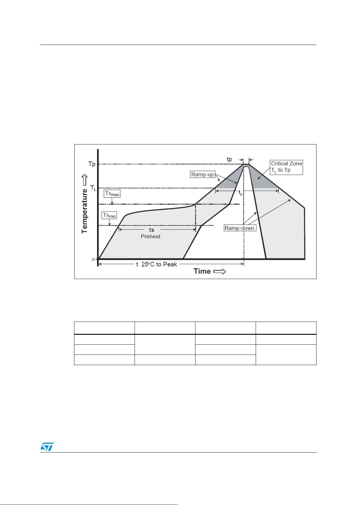
STAC packages. It is important that this profile, as shown in Figure 10, is respected at the
component level. According to table 4-2 of the JEDEC reference, a max Tp of 245 °C is
advised, but STAC packages can survive many reflows at temperatures up to a body
temperature of 265 °C with no damage. However, such excursions up to this extreme
temperature are not recommended because many other board level components may not
survive such stressful conditions.
Figure 10. Component level temperature profile
Note: Tp= 20-40 sec, ramp-up = 3 °C/sec max, T
217 °C, T
= 200 °C, T
Smax
= 150 °C, TS= 60-180 sec, from t 25 °C to peak = 8 minutes
Smin
max, tp = Ta bl e 5 .
Table 5. Pb-free process - package classification reflow temperatures
Package thickness Volume mm3 < 350 Volume mm3 350-2000 Volume mm3 > 2000
< 1.6 mm
1.6 mm - 2.5 mm 250 + 0 °C
> 2.5 mm 250 + 0 °C 245 + 0 °C
1. Tolerance: the device manufacturer/supplier assures process compatibility up to and including the stated
classification temperature (this means peak reflow temperature + 0 °C. For example 260 °C + 0 °C) at the
rated MSL level.
260 + 0 °C
Doc ID 17594 Rev 3 21/26
= 60-150 sec, ramp-down = 6 °C/sec max, TL=
L
(1)
260 + 0 °C 260 + 0 °C
245 + 0 °C
Page 22

Package attachment to thermal base by means of soldering AN3232
Note: The profiling tolerance is + 0 °C, -X °C (based on the machine variation capability)
regardless of what is required to control the profile process, but at no time does it exceed -5
°C. The producer assures process compatibility at the peak reflow temperatures.
Package volume excludes external terminals (balls, bumps, lands, leads) and/or nonintegral heatsinks.
The maximum component temperature reached during reflow depends on package
thickness and volume. The use of convection reflow processes reduces the thermal
gradients between packages. However, thermal gradients due to differences on thermal
mass of SMD packages may still exist.
Ultimately, the most stressful aspect of soldering for packaging consisting of plastic or epoxy
layers is related to rapid transition between process steps. For this reason, it is
recommended to never exceed the ramping rates recommended in J-STD-020D at the
package level.
22/26 Doc ID 17594 Rev 3
Page 23

AN3232 Electrical connection
11 Electrical connection
Leads and/or flanges should be attached to the PCB and/or copper heatsinks using typical
Sn63Pb37 or Pb-free solders, in accordance with the supplier's recommendations.
However, the following guidelines with respect to the package should be considered:
● Avoid, as much as possible, the use of flux or flux solutions as it is a potential source of
contamination to the device.
● The leads of the transistor may be tinned prior to assembly on the PCB. This practice is
used in situations when it is undesirable to introduce even a small amount of gold into
the solder composition, forestalling the possibility of solder embrittlement issues. The
source of Au stems from the lead and/or backside surfaces, which are plated with 40 to
100 µin (1 to 2.5 µm) of Au.
● The amount of solder to be used depends on the type of solder and the amount of
allowable Au in the final solder composition. It is desirable to increase the amount of
solder when Au content is a concern, such as in Pb-free soldering applications.
● It is recommended to use either a solder preform or solder paste having a thickness of
0.001 to 0.010 in (0.03 to 0.3 mm), typically 0.006 in (.15 mm).
● Adjustment of the solder preform or paste thickness may be used advantageously to
account for thickness variations in the PCB manufacturing process.
● In cases where the backside of the flange is soldered to a copper core or heatsink, the
package design and previously discussed mechanical mounting procedure provide
sufficient downward pressure on the solder preform, resulting in a thin, high-quality
bondline after a typical solder reflow procedure. In such cases, solder-wells or a soldermoat around the perimeter of the flange should be considered, to provide a region for
excess solder to flow.
● A solder preform or other metallic foil may be used as both a TIM and electrical
interface between the backside of the package (source) and amplifier ground (normally
the core layer or the heatsink) even without soldering.
● Electrically insulative thermal pastes must be applied sufficiently thin, such that the
downward pressure is high enough to force metal-to-metal contact over a significant
area of the surfaces between the package (source) and amplifier ground.
Doc ID 17594 Rev 3 23/26
Page 24

Conclusion AN3232
12 Conclusion
This application note provides a set of guidelines to be considered for the proper attachment
of STAC packages. While these recommendations are intended to address the majority of
user applications, the flexibility afforded by this new generation of package technology
enables new approaches for amplifier assembly as well as novel system architectures. In
the search for constant improvement, ST continues to address customer needs by
improving the robustness of the STAC package line and by releasing additional outlines with
more functionality and versatility. For these reasons, it is expected that these guidelines are
to be revisited and updated over time. At present, these recommendations are expected to
result in reliable mechanical, electrical, and thermal performance.
Regarding the thermal expectations of STAC packages, this application note demonstrates
the exceptional performance that can be attained when utilizing the solder-down mounting
method; this can be viewed as the limiting case for lowest achievable thermal resistance.
While the STAC package concept embodies highly customizable thermal solutions by
means of chip carrier material substitution, the importance of an exceptionally low thermal
resistance between the transistor case and the heatsink (R
the case presented, this interface accounts for only 0.025 °C/W, roughly half of what is
achievable with industry standard flanged packages. In this regard, STAC packages afford
intrinsic flatness and the highest available thermal conductivity materials, further enhancing
cooling efficiency. Even without soldering, judicious selection of TIMS and respect to this set
of guidelines results in R
values on the order of 0.05 °C/W.
thC-HS
) cannot be overstated. In
thC-HS
24/26 Doc ID 17594 Rev 3
Page 25

AN3232 Revision history
13 Revision history
27-Jul
Table 6. Document revision history
Date Revision Changes
03-Aug-2010 1 Initial release.
08-Jun-2011 2
31-Aug-2011 3 Introduction on cover page has been updated.
Updated Figure 7: Ideal screw-center spacing and Section 9.2:
Considerations.
Doc ID 17594 Rev 3 25/26
Page 26

AN3232
Please Read Carefully:
Information in this document is provided solely in connection with ST products. STMicroelectronics NV and its subsidiaries (“ST”) reserve the
right to make changes, corrections, modifications or improvements, to this document, and the products and services described herein at any
time, without notice.
All ST products are sold pursuant to ST’s terms and conditions of sale.
Purchasers are solely responsible for the choice, selection and use of the ST products and services described herein, and ST assumes no
liability whatsoever relating to the choice, selection or use of the ST products and services described herein.
No license, express or implied, by estoppel or otherwise, to any intellectual property rights is granted under this document. If any part of this
document refers to any third party products or services it shall not be deemed a license grant by ST for the use of such third party products
or services, or any intellectual property contained therein or considered as a warranty covering the use in any manner whatsoever of such
third party products or services or any intellectual property contained therein.
UNLESS OTHERWISE SET FORTH IN ST’S TERMS AND CONDITIONS OF SALE ST DISCLAIMS ANY EXPRESS OR IMPLIED
WARRANTY WITH RESPECT TO THE USE AND/OR SALE OF ST PRODUCTS INCLUDING WITHOUT LIMITATION IMPLIED
WARRANTIES OF MERCHANTABILITY, FITNESS FOR A PARTICULAR PURPOSE (AND THEIR EQUIVALENTS UNDER THE LAWS
OF ANY JURISDICTION), OR INFRINGEMENT OF ANY PATENT, COPYRIGHT OR OTHER INTELLECTUAL PROPERTY RIGHT.
UNLESS EXPRESSLY APPROVED IN WRITING BY TWO AUTHORIZED ST REPRESENTATIVES, ST PRODUCTS ARE NOT
RECOMMENDED, AUTHORIZED OR WARRANTED FOR USE IN MILITARY, AIR CRAFT, SPACE, LIFE SAVING, OR LIFE SUSTAINING
APPLICATIONS, NOR IN PRODUCTS OR SYSTEMS WHERE FAILURE OR MALFUNCTION MAY RESULT IN PERSONAL INJURY,
DEATH, OR SEVERE PROPERTY OR ENVIRONMENTAL DAMAGE. ST PRODUCTS WHICH ARE NOT SPECIFIED AS "AUTOMOTIVE
GRADE" MAY ONLY BE USED IN AUTOMOTIVE APPLICATIONS AT USER’S OWN RISK.
Resale of ST products with provisions different from the statements and/or technical features set forth in this document shall immediately void
any warranty granted by ST for the ST product or service described herein and shall not create or extend in any manner whatsoever, any
liability of ST.
ST and the ST logo are trademarks or registered trademarks of ST in various countries.
Information in this document supersedes and replaces all information previously supplied.
The ST logo is a registered trademark of STMicroelectronics. All other names are the property of their respective owners.
© 2011 STMicroelectronics - All rights reserved
STMicroelectronics group of companies
Australia - Belgium - Brazil - Canada - China - Czech Republic - Finland - France - Germany - Hong Kong - India - Israel - Italy - Japan -
Malaysia - Malta - Morocco - Philippines - Singapore - Spain - Sweden - Switzerland - United Kingdom - United States of America
www.st.com
26/26 Doc ID 17594 Rev 3
 Loading...