

Page 1

PCB design guidelines for the STM32W108 platform
1 Introduction
STMicroelectronics provides a IEEE 802.15.4 product design engineer with a number of
paths towards the successful design of a IEEE 802.15.4-compliant solution based on the
STMicroelectronics STM32W108 family of system-on-chip (SoC) platforms. The
STM32W108xx kits contain software, hardware, and documentation designed for
developers to create applications efficiently on a tested and controlled platform. Once the
design team is familiar with ST's STM32W108xx products and the available IEEE 802.15.4
software libraries and stacks, the next step in the design path involves designing applicationspecific hardware to meet product requirements.
This application note is intended to accompany the reference designs and provide detailed
information regarding the design decisions employed within STMicroelectronics designs. In
addition, it details the design guidelines for developing an application-specific IEEE 802.15.4
design using an STM32W108xx device.
AN3206
Application note
After reading this document, developers should be able to successfully implement a design
with an STM32W108xx device. For further information, visit the STMicroelectronics web site
at www.st.com/stm32w.
Due to the application-specific nature of STMicroelectronics reference designs, ST
recommends that hardware designers familiarize themselves with the most recent reference
design available. This document is applicable to the following STM32W108xx kits:
● STM32W108xx starter kit (part number: STM32W-SK)
● STM32W108xx extension kit (part number: STM32W-EXT)
● STM32W108xx low-cost RF control kit (part number: STM32W-RFCKIT)
Note: The STM32W108 Reference Design is built on a 4-layer, FR-4 epoxy PCB.
The STM32W108-based Reference Design includes the following elements:
■ Schematics (in PDF format)
■ Bill of materials (BOM)
■ Gerber files
While the Reference Design includes most of the information required to start an
application-specific design, if additional items needed, please contact STMicroelectronics
Customer Support on the STMicroelectronics web site www.st.com/stm32w.
March 2011 Doc ID 17406 Rev 3 1/14
www.st.com
Page 2

Contents AN3206
Contents
1 Introduction . . . . . . . . . . . . . . . . . . . . . . . . . . . . . . . . . . . . . . . . . . . . . . . . 1
2 Reference design . . . . . . . . . . . . . . . . . . . . . . . . . . . . . . . . . . . . . . . . . . . 3
2.1 RF design guidelines . . . . . . . . . . . . . . . . . . . . . . . . . . . . . . . . . . . . . . . . . 4
2.1.1 STM32W108 RF ports . . . . . . . . . . . . . . . . . . . . . . . . . . . . . . . . . . . . . . . 4
2.1.2 Optimizing for TX (Boost mode) . . . . . . . . . . . . . . . . . . . . . . . . . . . . . . . . 4
2.1.3 Matching network circuit design . . . . . . . . . . . . . . . . . . . . . . . . . . . . . . . . 5
2.1.4 Harmonic filter design . . . . . . . . . . . . . . . . . . . . . . . . . . . . . . . . . . . . . . . 8
2.1.5 Band-pass filter . . . . . . . . . . . . . . . . . . . . . . . . . . . . . . . . . . . . . . . . . . . . 8
2.1.6 Antenna matching circuit . . . . . . . . . . . . . . . . . . . . . . . . . . . . . . . . . . . . . 8
2.2 RF layout guidelines . . . . . . . . . . . . . . . . . . . . . . . . . . . . . . . . . . . . . . . . . . 9
2.2.1 PCB tolerance . . . . . . . . . . . . . . . . . . . . . . . . . . . . . . . . . . . . . . . . . . . . . 9
2.3 Other design considerations . . . . . . . . . . . . . . . . . . . . . . . . . . . . . . . . . . . . 9
3 Non-RF design considerations . . . . . . . . . . . . . . . . . . . . . . . . . . . . . . . 10
3.1 High-frequency (24-MHz) crystal reference (X1, C5, and C6) . . . . . . . . . 10
3.2 Optional Low-frequency crystal reference (X2, C27 and C26) . . . . . . . . . 11
3.3 1.8V regulator load capacitor . . . . . . . . . . . . . . . . . . . . . . . . . . . . . . . . . . 12
3.4 1.2V regulator loading . . . . . . . . . . . . . . . . . . . . . . . . . . . . . . . . . . . . . . . 12
3.5 1.8V net decoupling . . . . . . . . . . . . . . . . . . . . . . . . . . . . . . . . . . . . . . . . . 12
3.6 1.8V analog to 1.8V digital filtering . . . . . . . . . . . . . . . . . . . . . . . . . . . . . . 12
3.7 RF test connector . . . . . . . . . . . . . . . . . . . . . . . . . . . . . . . . . . . . . . . . . . . 13
4 Revision history . . . . . . . . . . . . . . . . . . . . . . . . . . . . . . . . . . . . . . . . . . . 13
2/14 Doc ID 17406 Rev 3
Page 3
AN3206 Reference design
2 Reference design
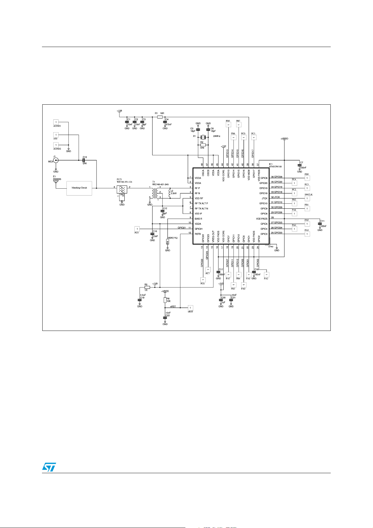
Figure 1 shows a block diagram of the reference design.
Figure 1. Block diagram of STM32W108 reference design (48-pin package)
The STM32W108 reference design uses an external 50/100 Balun as its primary RF
component. It provides an unbalanced to differential 50-to-100 Ohms conversion to present
the STM32W108 with its optimal load. A single inductor makes up the matching network and
optimizes RF performance. A band pass filter keeps the conducted harmonics within FCC
and ETSI limits.
Due to the market demand that IEEE 802.15.4 software maximize their communication
range, this design has been optimized accordingly. In Boost mode, the STM32W108
reference design achieves a high transmit output power across the 16 channels. This
section describes the design decisions behind each of the items shown in Figure 1.
Doc ID 17406 Rev 3 3/14
Page 4
Reference design AN3206
2.1 RF design guidelines
2.1.1 STM32W108 RF ports
The STM32W108's bi-directional RF port (pins RF_P and RF_N) provides access to a low
noise amplifier (LNA) and a power amplifier (PA) through a shared differential interface. The
disabled high-Z state of either the PA or the LNA enables transmitting and receiving through
the shared port without the need for a conventional T/R switch.
An ‘alternate’ PA-only port (pins RF_TX_ALT_P and RF_TX_ALT_N) is also provided. This
function is achieved via an additional PA. Design considerations for this alternate PA are not
covered in this document.
Note: The on-chip parasitic capacitance is different between the two ports and will slightly alter the
off-chip matching component values.
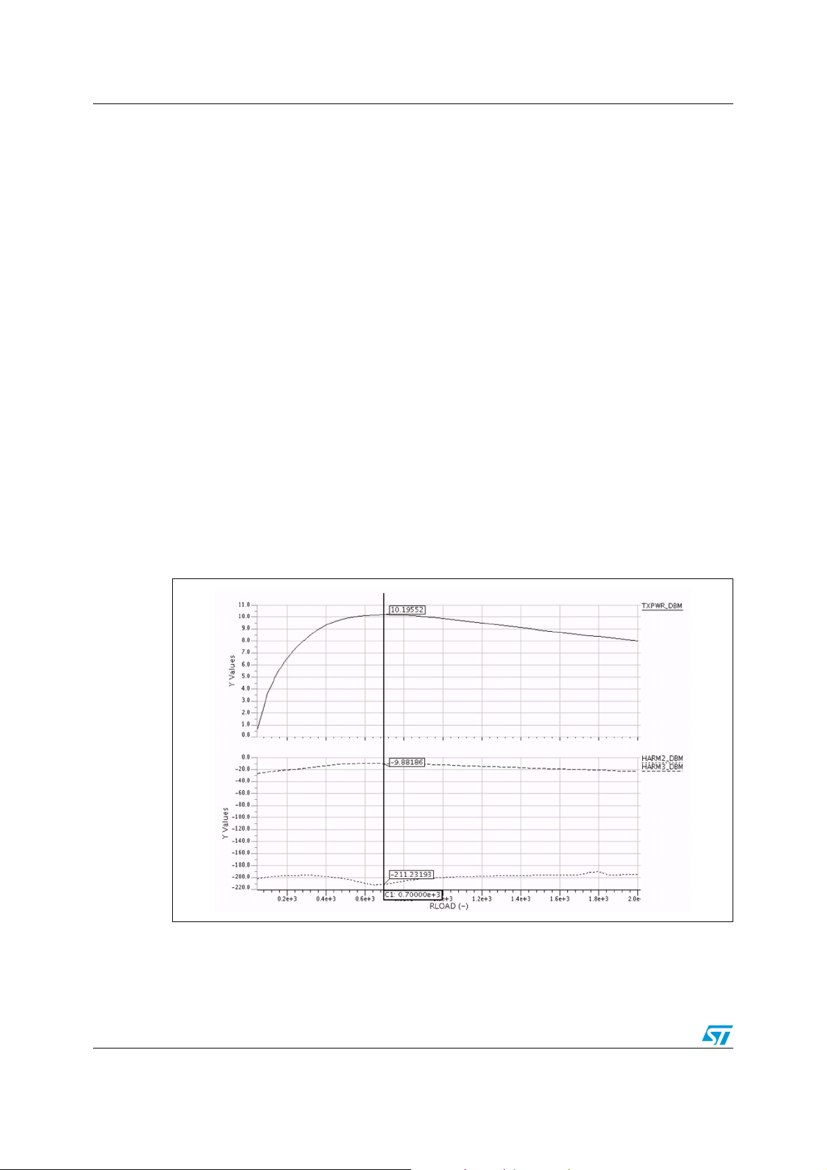
2.1.2 Optimizing for TX (Boost mode)
The STM32W Reference Design has been optimized for maximum transmitter (TX) output
power in Boost mode using practical components and readily available printed circuit board
(PCB) substrates. The optimum load at the PA on the silicon die is approximately 700Ω
when the PA/LNA device capacitance is resonated-out. This maximizes the voltage swing at
the drains of the PA devices within the available supply voltage. Too large a load causes
voltage limiting whereas too small a load does not make full use of the available supply
voltage. Figure 2 illustrates a die-level simulation of the load impedance and its effect on PA
output power.
Figure 2. Simulated Boost output power with PA load resistance
Optimizing the TX output performance in Boost mode does not cause degradation in either
Normal mode or RX sensitivity. Because the receiver is CMOS-based, it amplifies the input
signal voltage, rather than its current. The receiver noise is a fixed value of noise voltage
that may be referred to its input. It might be expected that increasing the transformation
4/14 Doc ID 17406 Rev 3
Page 5

AN3206 Reference design
would yield higher signal voltage swings at the LNA input, making the input referred noise
less significant and thereby improving sensitivity. However, this also increases the source
resistance, thereby increasing the source noise voltage. In practice at the 700Ω level, the
improvement gradient is very small and the transmit output power exhibits far greater
sensitivity to load variation than receiver sensitivity. The main objective for receive sensitivity
is to minimize network loss, which is a common objective when transmitting.
The optimum load presented to the pins of the STM32W108 device must take into
consideration not only the optimum PA load but also on-chip parasitic capacitance and
package bond-wire inductance. It is estimated that the optimum load presented to the pins is
27 + j95Ω (series impedance). This is equivalent to a parallel resistance of 368Ω combined
with a parallel inductance of 6.6 nH.
Optimal Load for STM32W (series impedance) 27 + j95 Ohms
2.1.3 Matching network circuit design
The term “matching” typically implies conjugate power matching. It is important to
understand that the STM32W PA is not power matched according to the traditional
definition. The term is used in this document to describe the design of an optimal PA
impedance.
The best way to understand ST's approach towards optimizing the STM32W “matching” is to
plot on the Smith chart the impedance of the ideal 700Ω PA load transformed by the
chip/package parasitic elements. The combination of the ideal load with the parasitic
elements is the conjugate of the ideal load presented to the package pins. Knowing the
combined load and its conjugate allows the designer to approach matching in a more
traditional sense, namely, “How do we get to 50Ω?”
It is also necessary at some point in the network to include a balanced-to-unbalanced
(balun) conversion. Use of a ‘proper’ balun has performance benefits related to commonmode suppression both on transmit and receive sides.
There are a variety of balun architectures and solutions available. The primary objective of
any of ST's reference designs is to minimize design complexity and maximize time to
market. Therefore, ST decided to implement its primary reference design with a ceramic
balun. The cost of ceramic baluns is low, and they are available from a number of vendors.
Ceramic baluns are available in 1:1 (50 to 50Ω), 2:1 (100 to 50Ω), and 4:1 ratios (200 to
50Ω).
The magnitude of the reflection coefficient, | ⎡
● 1:1 (50Ω) → 0.8
● 2:1 (100Ω) → 0.76
● 4:1 (200Ω) → 0.8
|, in these three cases is:
L
This implies that a 2:1 ceramic balun should offer the lowest network loss, assuming
identical balun loss because it requires the least transformation.
Investigation into ceramic balun performance from various vendors reveals that 1:1 and 2:1
ratio baluns often have an approximate 0.3 dB insertion loss advantage over a 4:1 ratio.
Thus the use of a 2:1 ceramic balun is preferred.
Doc ID 17406 Rev 3 5/14
Page 6

Reference design AN3206
To minimize network loss, the matching topology should try to keep Smith chart loci towards
the center of the Smith chart. To do that, the following impedance transformation options are
available:
● Series inductance followed by Shunt capacitance
– This option favors lower balun ratios.
– It leads to comparatively large inductance values.
– It requires either long PCB traces or two discrete inductors (balanced network)
which means inductor Q becomes an issue.
● Series inductance followed by Shunt inductance
– Similar to auto-transformer action.
– Sweet-spot for 100Ω balun if series inductance fabricated from PCB traces since
neither too long nor too short.
● Shunt inductance followed by series capacitance
– Not allowed because DC feed to PA is required from balun centre-tap.
● Shunt inductance followed by Series inductance
– Favors lower balun ratios, but even at 1:1 the required series inductance is
comparatively large.
– It requires either long PCB traces or two discrete inductors (balanced network)
which means inductor Q becomes an issue.
PCB parasitic elements play a part in the impedance transformation and even with the
tightest of layouts, traces between the matching elements will add significant reactance at
2.4 GHz. In particular, there will be some series inductance between the package pins and
the first matching element. This is significant when that element is shunted because it
cannot be absorbed into that reactance. Since this effect cannot be avoided, it is best to take
advantage of it.
The option with the lowest loss and least complex arrangement is series inductance
followed by shunt inductance. To make use of the PCB traces, it must be recognized that
they operate more like transmission lines which travel slightly differently on the Smith chart
compared with real inductors and this affects the shunt inductance value.
Traces of 100Ω which equate to 150um wide on a 0.4mm thick FR-4 substrate should be
used. In ST's simple single-ended representation in the Smith chart, the balanced pair must
be modeled as a single 200Ω transmission line. Figure 3 illustrates the impedance
transformation.
6/14 Doc ID 17406 Rev 3
Page 7

AN3206 Reference design
Figure 3. STM32W Ceramic Balun matching network
Figure 4 shows a PCB layout (layer 1). It is important that the PCB designer notice the
routes between the STM32W and the balun. ST recommends the use of an 0603 inductor to
allow ample space for the traces to go to the balun first with deterministic lengths. Trace
inductance between the inductor and balun is then absorbed into the total shunt inductance,
so it may be predictably offset by reducing the physical component value. The tuned value
on the reference design came out to be 3.3 nH.
Figure 4. Layer 1 except showing the balun routes
The PCB designer has the option to route the traces to the inductor first and the balun
second, but this has the effect of moving the components further away from the STM32W.
Doc ID 17406 Rev 3 7/14
Page 8

Reference design AN3206
By routing in this manner, PCB area and cost are wasted. It also requires the model to be
updated to a three-element match, generally making it more difficult to simulate.
An added benefit of using an 0603 inductor over an 0402 inductor is that better Q is
obtainable. The STM32W Ceramic Balun Reference Design uses a Murata LQG18H series
inductor which has a typical Q of approximately 100 at 2.4 GHz. Compare this to the
commonly used LQP15M 0402 inductor, which has a typical Q of approximately 50. This is
worth nearly 0.2 dB. The disadvantage is that it is not possible to get E24 values in 0603
style at these sorts of component values. So a small price is paid on design centering.
As previously mentioned, the balun center tap is fed with a 1.8V DC feed. A decoupling
capacitor is required to define the common-mode RF potential. The balun decoupling
capacitor needs to be as close as possible to the balun pins and with a high quality ground
connection. Its value is chosen to be series resonant with its parasitic inductance at 2.4GHz.
While it would be possible to tune-out longer tracks by using a smaller capacitor value, this
has the effect of making the decoupling more narrow-band, which can impact commonmode harmonic suppression.
2.1.4 Harmonic filter design
FCC Rule 15.35 allows for a duty-cycle relaxation to the regulatory limits. For EmberZNet
Pro, the relaxation is 6.9 dB.
FCC Rule 15.205 defines 'restricted bands' where harmonics must meet the levels set out in
FCC Rule 15.209. This is defined as -41.2 dBm/MHz up to 12.5 GHz. This applies to the
2nd, 3rd, and 5th harmonics, but not the 4th harmonic.
ETSI EN 300 440-1 requires spurious emissions to be less than -30 dBm/MHz,
1GHz~24GHz, so this becomes the default limit for the 4th harmonic.
Generally, if FCC limits are met it is extremely unlikely that harmonics to 24 GHz would fail
ETSI requirements, so frequencies above the 5th harmonic are not considered here.
The overall requirement is shown in Tabl e 1 .
Table 1. Harmonic power limits
Harmonic Frequency Limit
2nd 4810~4960 MHz
3rd 7215~7440 MHz
4th 9620~9920 MHz
5th 12025~12400 MHz
2.1.5 Band-pass filter
ST decided to use a band-pass filter as it is a convenient way to ensure that unwanted
harmonics are filtered out and 50 Ohms adaptation is guaranteed between the balun and
the antenna matching circuitry.
2.1.6 Antenna matching circuit
≤–34.3 dBm/MHz
≤–34.3 dBm/MHz
≤–30.0 dBm/MHz
≤–34.3 dBm/MHz
A matching circuit is needed to adapt the impedance between the 50-Ohm band-pass filter
and the antenna. Ideally a 50-Ohm trace should be enough, but, in reality, antenna
impedance varies with its environment. Once the antenna characteristics as been measured
8/14 Doc ID 17406 Rev 3
Page 9

AN3206 Reference design
using a vector network analyzer (VNA), it is easy to figure out with the help of a Smith chart
the value needed to compensate the de-adaptation. In our practical case, a serial capacitor
(C8) and inductor (L1) have been selected.
Figure 5. Antenna matching circuit
2.2 RF layout guidelines
At 2.4GHz it does not take much for a poorly designed PCB to build up enough parasitic
reactance to noticeably compromise RF performance. The following notes describe how the
PCB design was implemented and some of the pitfalls that could arise in transferring the
design to a product.
2.2.1 PCB tolerance
Volume manufacturing requires the least expensive materials to be used while meeting an
acceptable level of performance. The effects of component choice have already been
discussed, but the PCB also plays a major part in the matching network and so you must
consider its performance.
For the types of cost-sensitive applications targeted, a low-cost PCB substrate is mandatory,
which means using a standard FR-4 epoxy. But within the FR4 classification there are cost
trade-offs to be made against:
● Dissipation Factor, DF (also known as loss tangent, tanδ)
● Dielectric Constant, DK (also known as relative permittivity, ε
Generally, materials are split into 'standard loss' and 'low loss' categories, with a
corresponding cost penalty. Other product considerations such as flammability rating and
lead-free assembly will narrow these choices. These are beyond the scope of this
document.
Modern PCB manufacturing achieves very accurate etching and so this is not considered as
a performance variable. Z-axis expansion depends on the FR-4 material and does not alter
much between vendors' material.
2.3 Other design considerations
Please refer to Section 3 for the non-RF requirements of the STM32W-based design.
)
r
Doc ID 17406 Rev 3 9/14
Page 10
Non-RF design considerations AN3206
3 Non-RF design considerations
To operate properly, each STM32W Reference design contains additional, non-RF
components. These include a 24-MHz crystal, appropriate decoupling capacitors and RF
test point as well as an InSight Port connector.
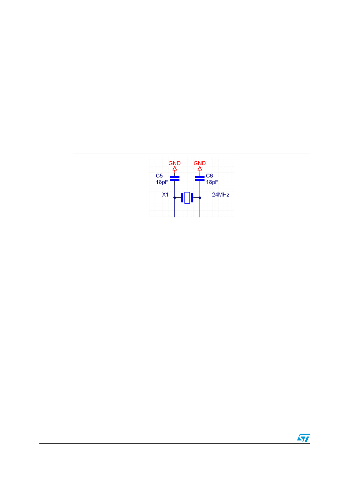
3.1 High-frequency (24-MHz) crystal reference (X1, C5, and C6)
The STM32W requires a single, accurate 24-MHz crystal source in order to develop the
proper STM32W clock distribution and IEEE 802.15.4 timing (see Figure 6).
Figure 6. 24MHz high-frequency crystal
ST recommends that the shunt loading capacitors, C5 and C6, be located fairly close
together and share a common ground via. The shunt capacitors and the crystal form a
resonant circuit with a reasonably high Q, so the circulating currents are high. As a result,
despite only consuming 1mA (for example), the circulating current through the shunt
capacitors may be several mA. If the grounds of the capacitors are widely separated, this
several mA loop current has to flow through the ground plane to get between the two
capacitors. The high current causes voltage to be developed due to the via inductance, as
well as potentially inducing a voltage in the ground plane. Bringing the capacitors closer
together means the majority of the loop current flows in surface tracks-only and an
imbalance current flows to ground, which should be small if the signal across the crystal is
symmetric and sinusoidal. It is difficult to say if this really makes a difference or not, and
capacitors are commonly taken to ground separately. However, the crystal is very near the
RF and the VCO in particular, and 24 MHz tones of the VCO are very detrimental, so the
problem is best avoided.
Due to the timing requirements of the IEEE 802.15.4-2003 Standard, this 24-MHz crystal
must meet an accuracy of ±40 ppm over tolerance, temperature, and aging. In addition, the
crystal must have a maximum ESR of 60Ω to control the integrated oscillator signal
strengths.
A manufacturing token within the STM32W device stores the crystal bias register setting.
This setting is automatically determined during PCB manufacturing testing when ST's
NodeTest or MFG Library software is used, and it is dependent upon the selected crystal.
For more information on this token, refer to application note AN3188: Preparing custom
devices for the STM32W108 platform. Loading capacitors C5 and C6 should be chosen
according to the crystal manufacturer's requirements.
10/14 Doc ID 17406 Rev 3
Page 11

AN3206 Non-RF design considerations
Table 2. High frequency crystal requirements
Parameter Test Conditions Min. Typ. Max. Unit
Frequency 24 MHz
Duty cycle 40 60 %
Phase noise from 1kHz to
100kHz
Accuracy
Crystal ESR Load capacitance of 10pF 100
Crystal ESR Load capacitance of 18pF 60
Start-up time to stable clock
(max. bias)
Start-up time to stable clock
(optimum bias)
Initial, temperature, and
aging
- 40 + 40 ppm
- 120 dBc/Hz
1ms
2ms
3.2 Optional Low-frequency crystal reference (X2, C27 and C26)
The STM32W contains an integrated sleep timer that allows for software configuration of
sleep/wake cycles of the wireless node. There are two options for driving the sleep timer: a
32.768 kHz crystal oscillator or an internal RC oscillator. The crystal oscillator is more
accurate but consumes more current than the RC oscillator. The RC oscillator is sufficient
for operating ST's IEEE 802.15.4 software libraries and stacks. Therefore, the application's
sleep timing accuracy will decide if a 32-kHz crystal is required.
Figure 7 illustrates the crystal oscillator with its loading capacitors. To reduce the effects of
overdriving the oscillator circuit within the STM32W, ST recommends an asymmetrical
loading of the crystal.
Figure 7. 32-kHz low-frequency crystal
If the application does not need the 32-kHz crystal, then the pins OSC32A (GPIO22) and
OSC32B (GPIO23) can be used as a general-purpose IO.
Doc ID 17406 Rev 3 11/14
Page 12
Non-RF design considerations AN3206
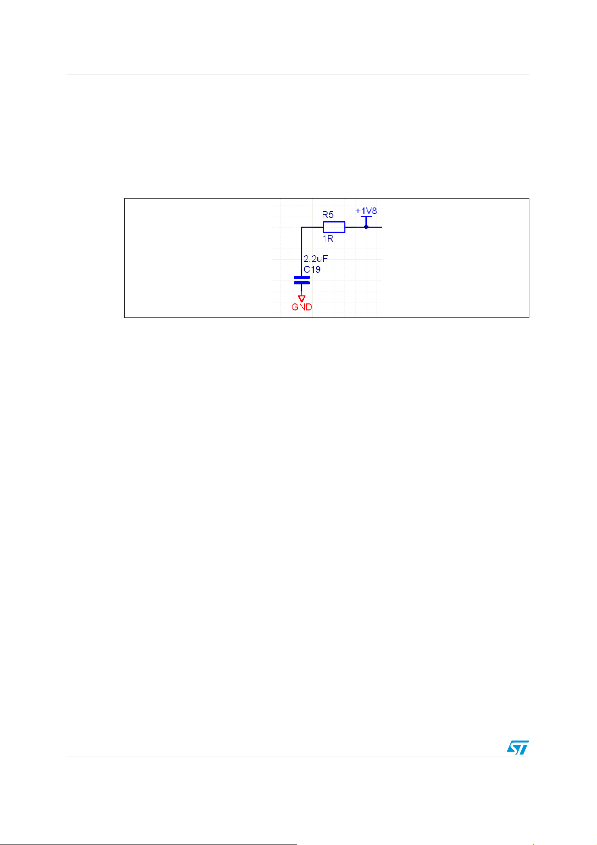
3.3 1.8V regulator load capacitor
The STM32W operates over a supply voltage (V
regulator converts V
2.2 µF ceramic loading capacitor is required on the output of VREG_OUT of the STM32W. A
series resistor (R5) is used to keep the minimum ESR of the loading capacitor below 1 Ohm.
This is shown in Figure 8.
Figure 8. 1.8V regulator loading capacitance
down to a trimmed 1.8V. To stabilize the integrated regulator, a
BRD
3.4 1.2V regulator loading
The STM32W contains an integrated 1.2V Regulator to drive the Core Logic. By driving the
core at this lower V
regulated voltage, a PCB designer should connect pin VDD_CORE_0 to pin VDD_CORE_1.
If you would like to drive the core at 1.8V, then the 1.8V net should be connected to both
pins VDD_CORE_0 and VDD_CORE_1.
potential, reduced current consumption is achieved. To utilize this
DD
) of 2.1 to 3.6V. An integrated 1.8V
BRD
A 1µF ceramic loading capacitor should be placed close to pin VDD_CORE_0. In addition, a
10nF decoupling capacitor should be place close to pin VDD_CORE_1.
3.5 1.8V net decoupling
To minimize noise and coupling paths into the STM32W, decoupling capacitors must be
placed on each of the VDD pins. All decoupling capacitors should be placed as close to the
STM32W as possible as well as in between the source point (via) and the STM32W pin. In
addition, all values should be maintained as defined by the STM32W Reference Design.
3.6 1.8V analog to 1.8V digital filtering
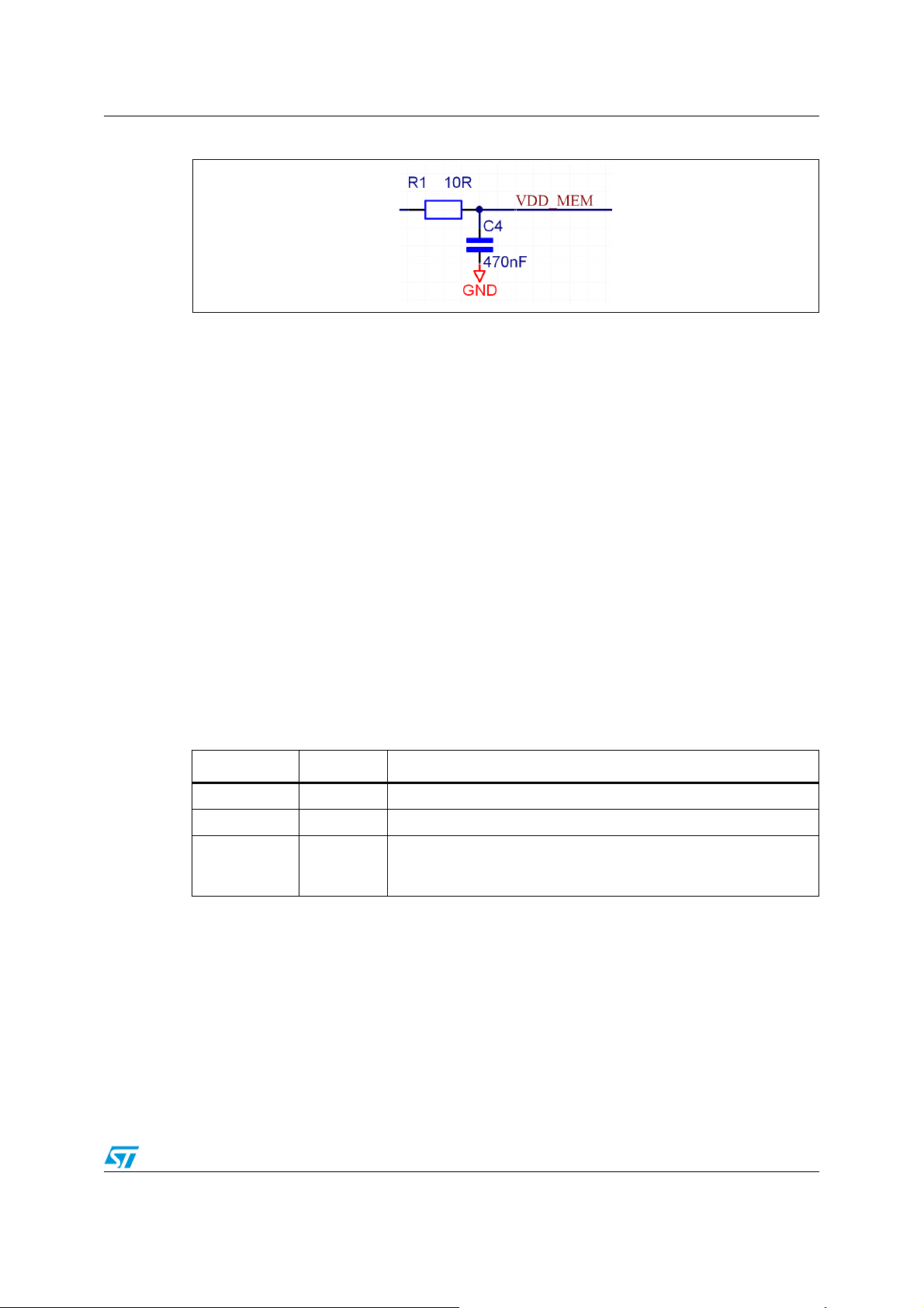
To keep the Radio Active current at 36 mA, ST recommends adding a single element filter
(resistor) between the digital and analog 1.8V nets, 1.8V_A and 1.8V_D, respectively (see
Figure 9). This resistor maintains a reduced bias current for the digital logic within the
STM32W. If this resistor is not used, the RX current will increase by 1mA to 37mA.
12/14 Doc ID 17406 Rev 3
Page 13
AN3206 Revision history
Figure 9. Digital VDD filter
The lower current consumption also allows for a reduction in the digital 1.8V Domain noise.
This means the RX sensitivity improves by 2dB when using the 10-Ohm resistor.
3.7 RF test connector
To assist with manufacturing testing of the printed circuit assemblies, ST recommends
having the possibility to solder an UF.L type RF connector such as those from Hirose.
After reading this document
If you have questions or require assistance with the procedures described in this document,
please contact STMicroelectronics support at http://www.st.com/stm32w.
4 Revision history
Table 3. Document revision history
Date Revision Changes
29-Apr-2010 1 Initial release.
08-Dec-2010 2 Updated Section 3.4: 1.2V regulator loading on page 12.
16-Mar-2011 3
Added support for STM32W108xx kits; updated “ZigBee” and
“EmberZNet” references with “IEEE 802.15.4”; and updated
STM32W website URL.
Doc ID 17406 Rev 3 13/14
Page 14

AN3206
Please Read Carefully:
Information in this document is provided solely in connection with ST products. STMicroelectronics NV and its subsidiaries (“ST”) reserve the
right to make changes, corrections, modifications or improvements, to this document, and the products and services described herein at any
time, without notice.
All ST products are sold pursuant to ST’s terms and conditions of sale.
Purchasers are solely responsible for the choice, selection and use of the ST products and services described herein, and ST assumes no
liability whatsoever relating to the choice, selection or use of the ST products and services described herein.
No license, express or implied, by estoppel or otherwise, to any intellectual property rights is granted under this document. If any part of this
document refers to any third party products or services it shall not be deemed a license grant by ST for the use of such third party products
or services, or any intellectual property contained therein or considered as a warranty covering the use in any manner whatsoever of such
third party products or services or any intellectual property contained therein.
UNLESS OTHERWISE SET FORTH IN ST’S TERMS AND CONDITIONS OF SALE ST DISCLAIMS ANY EXPRESS OR IMPLIED
WARRANTY WITH RESPECT TO THE USE AND/OR SALE OF ST PRODUCTS INCLUDING WITHOUT LIMITATION IMPLIED
WARRANTIES OF MERCHANTABILITY, FITNESS FOR A PARTICULAR PURPOSE (AND THEIR EQUIVALENTS UNDER THE LAWS
OF ANY JURISDICTION), OR INFRINGEMENT OF ANY PATENT, COPYRIGHT OR OTHER INTELLECTUAL PROPERTY RIGHT.
UNLESS EXPRESSLY APPROVED IN WRITING BY AN AUTHORIZED ST REPRESENTATIVE, ST PRODUCTS ARE NOT
RECOMMENDED, AUTHORIZED OR WARRANTED FOR USE IN MILITARY, AIR CRAFT, SPACE, LIFE SAVING, OR LIFE SUSTAINING
APPLICATIONS, NOR IN PRODUCTS OR SYSTEMS WHERE FAILURE OR MALFUNCTION MAY RESULT IN PERSONAL INJURY,
DEATH, OR SEVERE PROPERTY OR ENVIRONMENTAL DAMAGE. ST PRODUCTS WHICH ARE NOT SPECIFIED AS "AUTOMOTIVE
GRADE" MAY ONLY BE USED IN AUTOMOTIVE APPLICATIONS AT USER’S OWN RISK.
Resale of ST products with provisions different from the statements and/or technical features set forth in this document shall immediately void
any warranty granted by ST for the ST product or service described herein and shall not create or extend in any manner whatsoever, any
liability of ST.
ST and the ST logo are trademarks or registered trademarks of ST in various countries.
Information in this document supersedes and replaces all information previously supplied.
The ST logo is a registered trademark of STMicroelectronics. All other names are the property of their respective owners.
© 2011 STMicroelectronics - All rights reserved
STMicroelectronics group of companies
Australia - Belgium - Brazil - Canada - China - Czech Republic - Finland - France - Germany - Hong Kong - India - Israel - Italy - Japan -
Malaysia - Malta - Morocco - Philippines - Singapore - Spain - Sweden - Switzerland - United Kingdom - United States of America
www.st.com
14/14 Doc ID 17406 Rev 3
 Loading...