

Page 1
AN3203
Application note
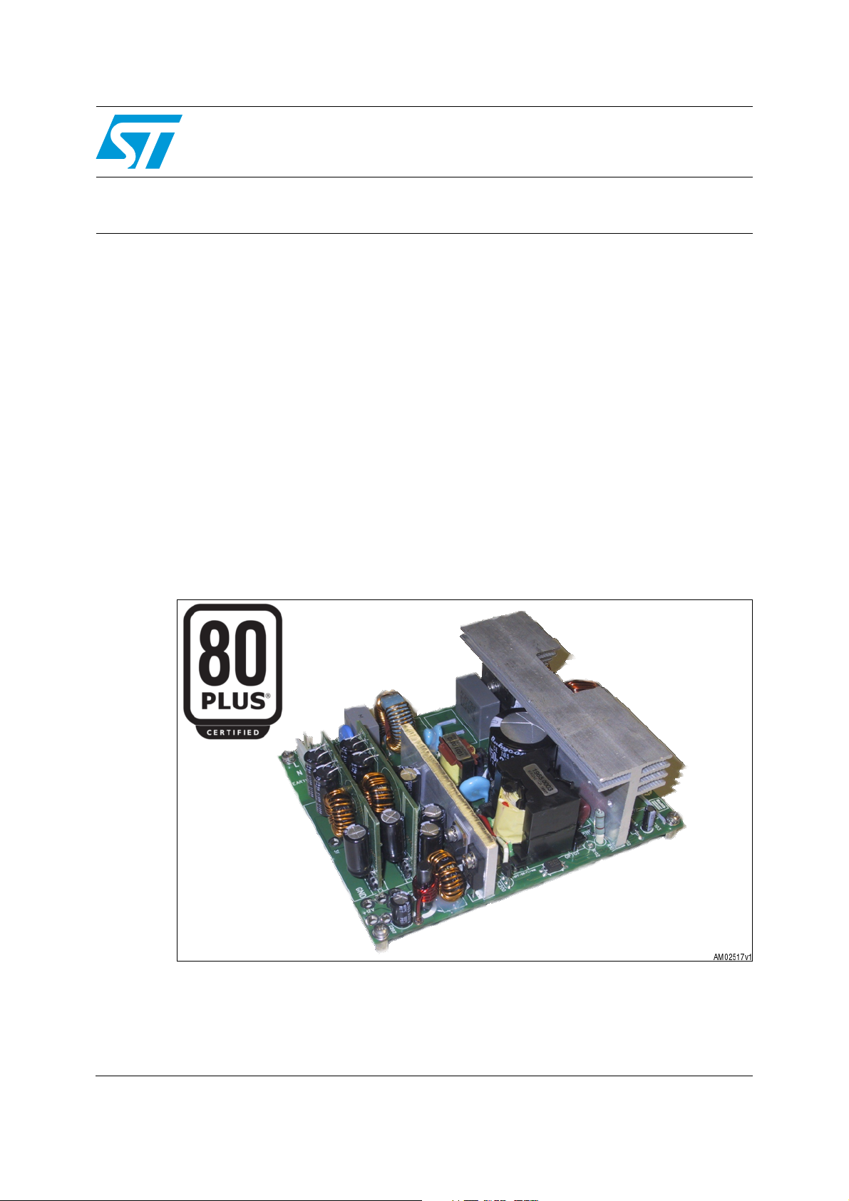
EVL250W-ATX80PL: 250W ATX SMPS
demonstration board
Introduction
This application note describes the characteristics and performance of a 250 W wide range
input and power factor corrected power supply designed to be used in an ATX application.
Good electrical performance allows meeting the most demanding efficiency targets.
The converter consists of four main blocks:
■ A PFC front-end stage using the L6563S PFC controller which generates the +400 V bus
voltage.
■ An AHB (Asymmetrical half bridge) stage using the L6591 ZVS half bridge controller
which performs the conversion from the high voltage bus to the +12 V output providing
insulation.
■ Two DC-DC post-regulator stages using the L6727 which obtain the +5 V and +3.3 V
outputs from the +12 V bus.
■ An auxiliary power supply (STANDBY) stage using the VIPer27H in isolated flyback
configuration which provides the +5 V_SB output with 10 W power capability.
Figure 1. 250 W ATX SMPS demonstration board
January 2011 Doc ID 17402 Rev 2 1/49
www.st.com
Page 2

Contents AN3203
Contents
1 Main characteristics and circuit description . . . . . . . . . . . . . . . . . . . . . 5
2 Asymmetrical half bridge operation . . . . . . . . . . . . . . . . . . . . . . . . . . . 12
2.1 AHB typical waveforms . . . . . . . . . . . . . . . . . . . . . . . . . . . . . . . . . . . . . . . 12
2.2 Short-circuit protection . . . . . . . . . . . . . . . . . . . . . . . . . . . . . . . . . . . . . . . 16
3 Complete system . . . . . . . . . . . . . . . . . . . . . . . . . . . . . . . . . . . . . . . . . . . 17
3.1 Overvoltage protection . . . . . . . . . . . . . . . . . . . . . . . . . . . . . . . . . . . . . . . 17
3.2 Load transients . . . . . . . . . . . . . . . . . . . . . . . . . . . . . . . . . . . . . . . . . . . . . 17
3.3 Standby operation . . . . . . . . . . . . . . . . . . . . . . . . . . . . . . . . . . . . . . . . . . 18
4 Electrical performance . . . . . . . . . . . . . . . . . . . . . . . . . . . . . . . . . . . . . . 19
4.1 Efficiency measurement and no-load consumption . . . . . . . . . . . . . . . . . 19
4.2 Thermal considerations . . . . . . . . . . . . . . . . . . . . . . . . . . . . . . . . . . . . . . 24
4.3 Harmonic content measurement . . . . . . . . . . . . . . . . . . . . . . . . . . . . . . . 25
4.4 Single output configuration . . . . . . . . . . . . . . . . . . . . . . . . . . . . . . . . . . . . 27
5 Conducted noise measurements (pre-compliance test) . . . . . . . . . . . 30
6 Parts list . . . . . . . . . . . . . . . . . . . . . . . . . . . . . . . . . . . . . . . . . . . . . . . . . . 32
7 PFC coil specification . . . . . . . . . . . . . . . . . . . . . . . . . . . . . . . . . . . . . . . 40
7.1 Electrical characteristics . . . . . . . . . . . . . . . . . . . . . . . . . . . . . . . . . . . . . . 40
8 AHB transformer specification . . . . . . . . . . . . . . . . . . . . . . . . . . . . . . . 41
8.1 Electrical characteristics . . . . . . . . . . . . . . . . . . . . . . . . . . . . . . . . . . . . . . 41
8.2 Mechanical aspect and pin numbering . . . . . . . . . . . . . . . . . . . . . . . . . . . 42
9 AUX flyback transformer specification . . . . . . . . . . . . . . . . . . . . . . . . . 44
9.1 Electrical characteristics . . . . . . . . . . . . . . . . . . . . . . . . . . . . . . . . . . . . . . 44
9.2 Mechanical aspect and pin numbering . . . . . . . . . . . . . . . . . . . . . . . . . . . 46
10 PCB layout . . . . . . . . . . . . . . . . . . . . . . . . . . . . . . . . . . . . . . . . . . . . . . . . 47
11 Revision history . . . . . . . . . . . . . . . . . . . . . . . . . . . . . . . . . . . . . . . . . . . 48
2/49 Doc ID 17402 Rev 2
Page 3

AN3203 List of tables
List of tables
Table 1. Efficiency @ 115 Vrms . . . . . . . . . . . . . . . . . . . . . . . . . . . . . . . . . . . . . . . . . . . . . . . . . . . . 19
Table 2. Efficiency @ 230 Vrms . . . . . . . . . . . . . . . . . . . . . . . . . . . . . . . . . . . . . . . . . . . . . . . . . . . . 19
Table 3. 80 PLUS® program efficiency levels (115Vac). . . . . . . . . . . . . . . . . . . . . . . . . . . . . . . . . . 19
Table 4. 80 PLUS® program efficiency levels (230 Vac) . . . . . . . . . . . . . . . . . . . . . . . . . . . . . . . . . 20
Table 5. Climate Savers Computing Initiative (for multi-output PSU) . . . . . . . . . . . . . . . . . . . . . . . . 20
Table 6. No-load consumption . . . . . . . . . . . . . . . . . . . . . . . . . . . . . . . . . . . . . . . . . . . . . . . . . . . . . 20
Table 7. Low load efficiency @ 115 Vrms . . . . . . . . . . . . . . . . . . . . . . . . . . . . . . . . . . . . . . . . . . . . 22
Table 8. Low load efficiency @ 230 Vrms . . . . . . . . . . . . . . . . . . . . . . . . . . . . . . . . . . . . . . . . . . . . 22
Table 9. PF vs. load . . . . . . . . . . . . . . . . . . . . . . . . . . . . . . . . . . . . . . . . . . . . . . . . . . . . . . . . . . . . . 26
Table 10. Single output efficiency @ 115 Vac . . . . . . . . . . . . . . . . . . . . . . . . . . . . . . . . . . . . . . . . . . 27
Table 11. Single output efficiency @ 230 Vac . . . . . . . . . . . . . . . . . . . . . . . . . . . . . . . . . . . . . . . . . . 27
Table 12. AHB efficiency with 400 Vdc input . . . . . . . . . . . . . . . . . . . . . . . . . . . . . . . . . . . . . . . . . . . 29
Table 13. EVL250W-ATX80PL bill of materials . . . . . . . . . . . . . . . . . . . . . . . . . . . . . . . . . . . . . . . . . 32
Table 14. Winding characteristics. . . . . . . . . . . . . . . . . . . . . . . . . . . . . . . . . . . . . . . . . . . . . . . . . . . . 40
Table 15. Winding characteristics. . . . . . . . . . . . . . . . . . . . . . . . . . . . . . . . . . . . . . . . . . . . . . . . . . . . 42
Table 16. Winding characteristics. . . . . . . . . . . . . . . . . . . . . . . . . . . . . . . . . . . . . . . . . . . . . . . . . . . . 45
Table 17. Document revision history . . . . . . . . . . . . . . . . . . . . . . . . . . . . . . . . . . . . . . . . . . . . . . . . . 48
Doc ID 17402 Rev 2 3/49
Page 4

List of figures AN3203
List of figures
Figure 1. 250 W ATX SMPS demonstration board . . . . . . . . . . . . . . . . . . . . . . . . . . . . . . . . . . . . . . . 1
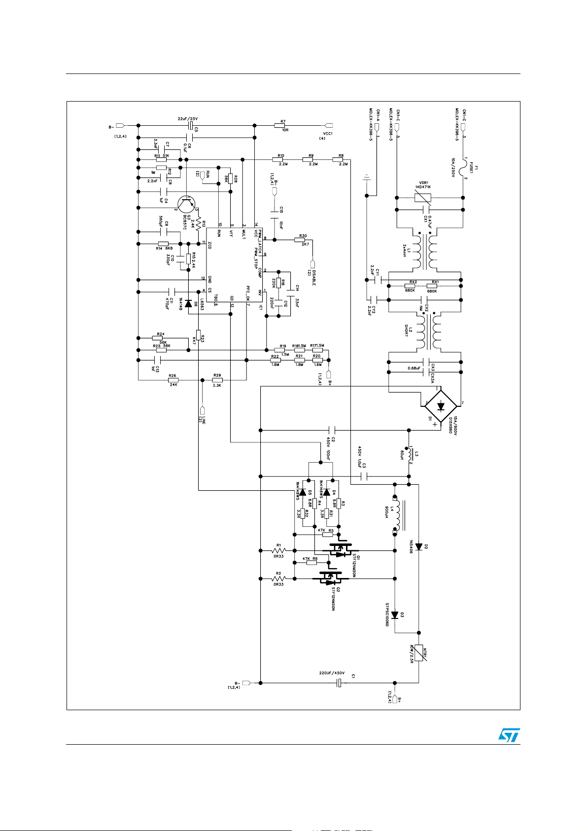
Figure 2. Electrical diagram: input EMI filter and PFC stage . . . . . . . . . . . . . . . . . . . . . . . . . . . . . . . . 8
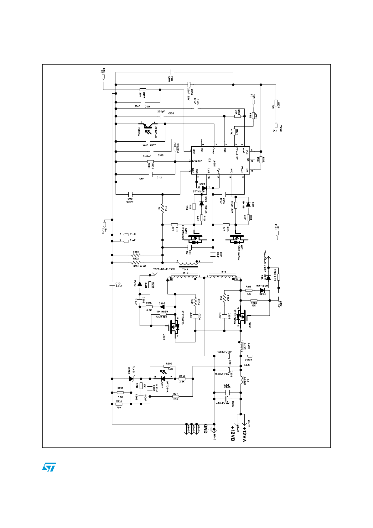
Figure 3. Electrical diagram: AHB stage . . . . . . . . . . . . . . . . . . . . . . . . . . . . . . . . . . . . . . . . . . . . . . . 9
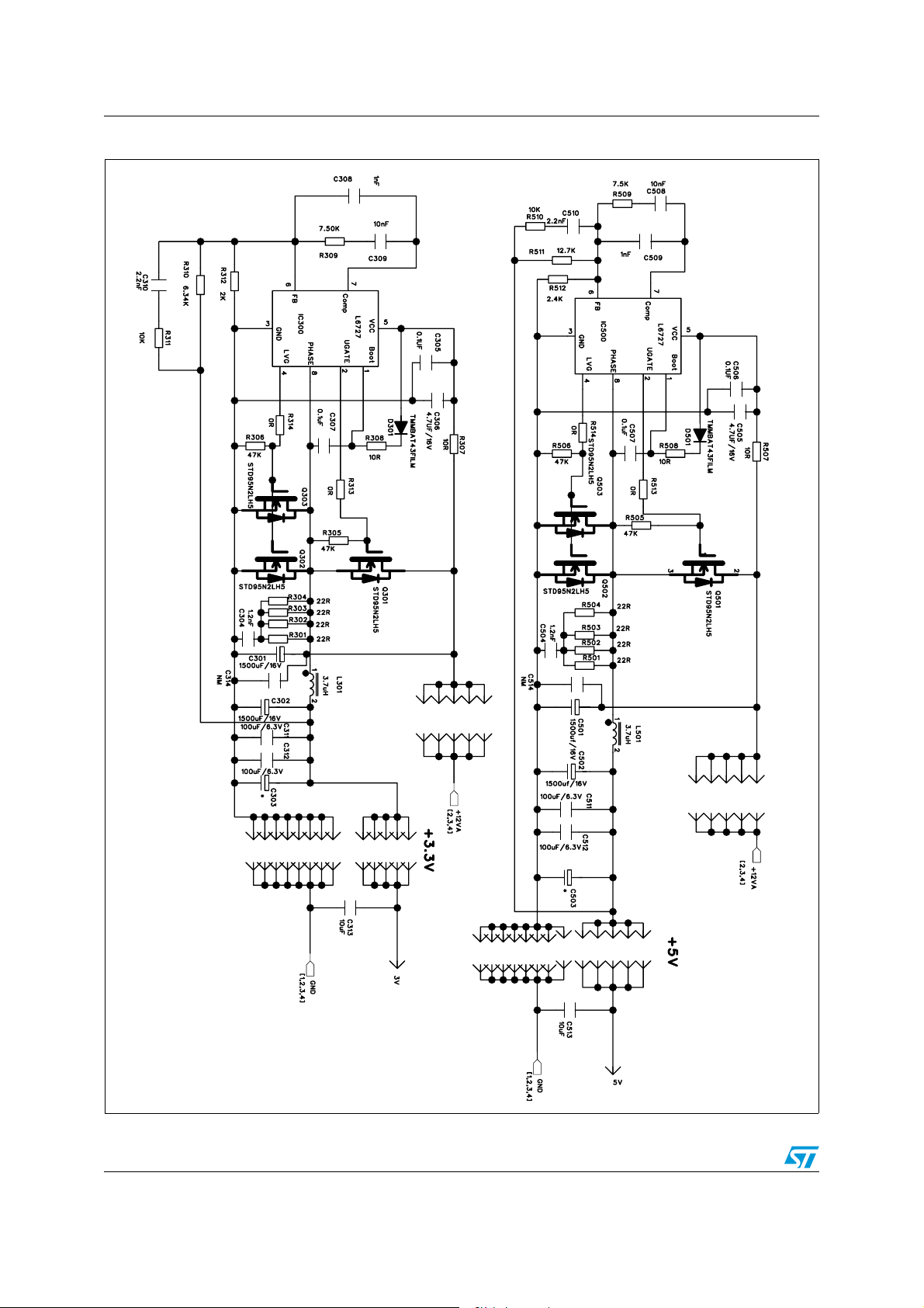
Figure 4. Electrical diagram: DC-DC stage . . . . . . . . . . . . . . . . . . . . . . . . . . . . . . . . . . . . . . . . . . . . 10
Figure 5. Electrical diagram: standby stage . . . . . . . . . . . . . . . . . . . . . . . . . . . . . . . . . . . . . . . . . . . . 11
Figure 6. AHB primary side key waveforms @ full load. . . . . . . . . . . . . . . . . . . . . . . . . . . . . . . . . . . 12
Figure 7. AHB zero voltage switching detail @ full load . . . . . . . . . . . . . . . . . . . . . . . . . . . . . . . . . . 13
Figure 8. AHB transitions detail @ 20 % rated load. . . . . . . . . . . . . . . . . . . . . . . . . . . . . . . . . . . . . . 14
Figure 9. AHB secondary side key waveforms @ full load . . . . . . . . . . . . . . . . . . . . . . . . . . . . . . . . 15
Figure 10. Short-circuit behavior detail . . . . . . . . . . . . . . . . . . . . . . . . . . . . . . . . . . . . . . . . . . . . . . . . 16
Figure 11. Load transient on +12 V output . . . . . . . . . . . . . . . . . . . . . . . . . . . . . . . . . . . . . . . . . . . . . 17
Figure 12. Load transient on +5 V output. . . . . . . . . . . . . . . . . . . . . . . . . . . . . . . . . . . . . . . . . . . . . . . 18
Figure 13. Load transient on +3.3 V output . . . . . . . . . . . . . . . . . . . . . . . . . . . . . . . . . . . . . . . . . . . . . 18
Figure 14. Efficiency vs. O/P power @ 115 Vac . . . . . . . . . . . . . . . . . . . . . . . . . . . . . . . . . . . . . . . . . 21
Figure 15. Efficiency vs. O/P power @ 230 Vac . . . . . . . . . . . . . . . . . . . . . . . . . . . . . . . . . . . . . . . . . 21
Figure 16. No-load consumption . . . . . . . . . . . . . . . . . . . . . . . . . . . . . . . . . . . . . . . . . . . . . . . . . . . . . 21
Figure 17. Efficiency at low loads . . . . . . . . . . . . . . . . . . . . . . . . . . . . . . . . . . . . . . . . . . . . . . . . . . . . 23
Figure 18. Fanless board . . . . . . . . . . . . . . . . . . . . . . . . . . . . . . . . . . . . . . . . . . . . . . . . . . . . . . . . . . . 24
Figure 19. EN61000-3-2 and JEITA-MITI measurements @ full load . . . . . . . . . . . . . . . . . . . . . . . . . 25
Figure 20. EN61000-3-2 and JEITA-MITI measurements @ 75 W in . . . . . . . . . . . . . . . . . . . . . . . . . 25
Figure 21. PF vs. input voltage . . . . . . . . . . . . . . . . . . . . . . . . . . . . . . . . . . . . . . . . . . . . . . . . . . . . . . 26
Figure 22. THD vs. input voltage . . . . . . . . . . . . . . . . . . . . . . . . . . . . . . . . . . . . . . . . . . . . . . . . . . . . . 26
Figure 23. Single output efficiency @ 115 Vac . . . . . . . . . . . . . . . . . . . . . . . . . . . . . . . . . . . . . . . . . . 28
Figure 24. Single output efficiency @ 230 Vac . . . . . . . . . . . . . . . . . . . . . . . . . . . . . . . . . . . . . . . . . . 28
Figure 25. AHB stage only efficiency (Vin = 400 Vdc) . . . . . . . . . . . . . . . . . . . . . . . . . . . . . . . . . . . . . 29
Figure 26. CE peak measurement@115 Vac and full load . . . . . . . . . . . . . . . . . . . . . . . . . . . . . . . . . 30
Figure 27. CE peak measurement @ 230 Vac and full load . . . . . . . . . . . . . . . . . . . . . . . . . . . . . . . . 30
Figure 28. CE average measurement@115 Vac and full load. . . . . . . . . . . . . . . . . . . . . . . . . . . . . . . 31
Figure 29. CE average measurement@230 Vac and full load. . . . . . . . . . . . . . . . . . . . . . . . . . . . . . . 31
Figure 30. Electrical diagram . . . . . . . . . . . . . . . . . . . . . . . . . . . . . . . . . . . . . . . . . . . . . . . . . . . . . . . . 40
Figure 31. Mechanical drawing (unit: mm) . . . . . . . . . . . . . . . . . . . . . . . . . . . . . . . . . . . . . . . . . . . . . . 40
Figure 32. Electrical diagram . . . . . . . . . . . . . . . . . . . . . . . . . . . . . . . . . . . . . . . . . . . . . . . . . . . . . . . . 41
Figure 33. Windings position . . . . . . . . . . . . . . . . . . . . . . . . . . . . . . . . . . . . . . . . . . . . . . . . . . . . . . . . 42
Figure 34. Bottom view . . . . . . . . . . . . . . . . . . . . . . . . . . . . . . . . . . . . . . . . . . . . . . . . . . . . . . . . . . . . 43
Figure 35. Electrical diagram . . . . . . . . . . . . . . . . . . . . . . . . . . . . . . . . . . . . . . . . . . . . . . . . . . . . . . . . 44
Figure 36. Windings position . . . . . . . . . . . . . . . . . . . . . . . . . . . . . . . . . . . . . . . . . . . . . . . . . . . . . . . . 45
Figure 37. Bottom view . . . . . . . . . . . . . . . . . . . . . . . . . . . . . . . . . . . . . . . . . . . . . . . . . . . . . . . . . . . . 46
Figure 38. Top side silk screen and copper . . . . . . . . . . . . . . . . . . . . . . . . . . . . . . . . . . . . . . . . . . . . . 47
Figure 39. Bottom side silk screen and copper (mirror view). . . . . . . . . . . . . . . . . . . . . . . . . . . . . . . . 47
4/49 Doc ID 17402 Rev 2
Page 5

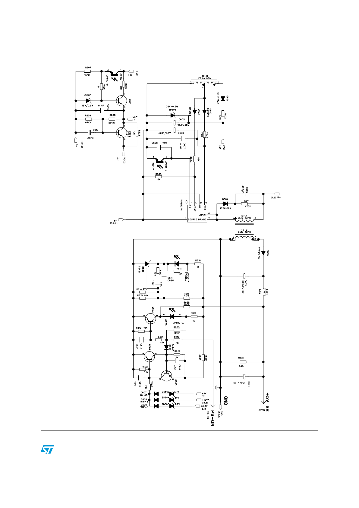
AN3203 Main characteristics and circuit description
1 Main characteristics and circuit description
Here are the main characteristics of the power supply:
● Input mains range:
– Vin: 88 ~ 264 Vrms
– f: 45 ~ 66 Hz
● Outputs:
– +12 Vdc ± 2 % - 13.5 A
– +5 Vdc ± 2 % - 12 A
– +3.3 Vdc ± 2 % - 8 A
– +5 V_SB ± 2 % - 2 A
● Standby consumption: < 0.2 W
● Protection:
– Short-circuit
–Overload
– Output overvoltage
– Brownout
● PCB type and size:
–FR4
– Double side CU 70 µm
– 148 x 120 mm
● Safety: according to EN60950
● EMI: according to EN55022 - class B
The EVL250W-ATX80PL demonstration board is made up of four main blocks, the
schematics are shown in Figure 2, 3, 4, and 5.
The front-end PFC stage is realized using a boost topology working in line modulated fixed
off time (LM-FOT) mode, described in STMicroelectronics’ application notes, AN1792;
Design of Fixed-Off-Time controlled PFC pre-regulators with the L6562 and AN3142;
Solution for designing a 400 W Fixed-Off-Time controlled PFC preregulator with the L6563S
and L6563H. The LM-FOT operation offers the advantage of having CCM operation (with
lower rms current with respect to TM mode) without the need to use a complex and
expensive controller. Therefore, it is possible to use the simple L6563S, enhanced TM PFC
controller, which integrates all the functions and protection, needed to control the stage, and
an interface with the downstream DC-DC converter.
The power stage of the PFC is realized with inductor L4, MOSFET Q1 and Q2, diode D3,
and capacitor C1. The LM-FOT operation is obtained with components D6, R15, C10, R14,
C9, R13, and Q3.
The PFC delivers a stable high voltage bus (+400 V nominal) to the downstream converters
(AHB and flyback) and provides for the reduction of the current harmonics drawn from the
mains, in order to meet the requirements of the European EN61000-3-2 norm and the
Japanese JEITA-MITI norm.
The second stage is an asymmetrical half bridge converter, driven by the L6591, a
STMicroelectronics controller dedicated to this topology. This IC integrates all the functions
Doc ID 17402 Rev 2 5/49
Page 6

Main characteristics and circuit description AN3203
and protection needed by the AHB stage and an interface for the PFC controller. The L6591
includes two gate drivers for the half bridge MOSFETs and a fixed frequency
complementary PWM logic with 50 % maximum duty cycle with programmable dead time
and current mode control technique.
Other features of this IC are pulse-by-pulse overcurrent protection, transformer saturation
detection, overload protection (latched or auto-restart), and programmable soft-start. There
is also a high voltage startup circuit, a burst mode logic for low load operation, and the
adaptive UVLO onboard, which are not used in this design as they are designed for adapter
applications (see AN2852).
The following is a description of the power circuit of this stage. The half bridge switches
Q101 and Q102 are connected to the output voltage of the PFC. The half bridge node drives
the series of C101 (DC blocking capacitor) and the primary side of the transformer T1. This
transformer has two secondary windings with a center tap connected to the secondary
ground. The other ends are connected to the sources of MOSFETs Q201 and Q202, which
replace output diodes in order to perform the synchronous rectification. Two extra windings
allow, with few external passive components, a self driven synchronous rectification to be
obtained. This solution allows efficiency to be increased without the extra cost of a
dedicated SR controller IC.
Q201 and Q202 drains are connected to the output inductor L201 that, together with output
capacitors C201 and C202, acts as a low pass filter. The signal +12 VA is then post filtered
(with L5 and C207) to obtain the +12 V output voltage.
The design of transformer T1 is a trade-off between ZVS operation and the required
electrical performance/efficiency. ZVS can be obtained acting on the magnetizing
inductance or on the primary side leakage inductance. In more detail, ZVS could be met by:
● Decreasing the magnetizing inductance
● Increasing the leakage inductance
Low values of magnetizing inductance generate high magnetizing current. This helps to
reach ZVS but it also increases the total primary side rms current and therefore the related
losses. In this design a value of 500 µH has been selected.
On the other hand, ZVS could be obtained by increasing the leakage inductance. If such a
parameter is increased, the primary side current takes more time before reversing its
direction and therefore ZVS is more easily met. A high leakage inductance value leads to
duty cycle losses, reducing the effective range of duty cycle usable. This creates problems
with hold-up requirements and makes it necessary to work with very narrow duty cycles with
nominal input voltage generating high rms currents in the circuit.
A value of 12 µH has been selected as the leakage inductance.
Because of these reasons, in this design ZVS is always met at low side MOSFET turn-on
while it is met only for medium-high loads at high side MOSFET turn-on. Even at mediumlow loads Q101 is turned on with a Vds well below the half bridge input voltage.
The L6591 LINE pin is used for startup sequencing. It shares with the L6563S the voltage
divider made up of R20, R21, R22, R29, and R26 that senses the PFC output voltage. The
AHB stage is activated when the bulk voltage reaches about 380 V.
The DISABLE pin (latched protection) is driven by the L6563S PWM_LATCH pin and stops
the AHB stage in case of PFC feedback disconnection.
The oscillator is programmed in order to have a switching frequency of about 80 KHz and to
use the minimum dead time (about 310 ns).
6/49 Doc ID 17402 Rev 2
Page 7

AN3203 Main characteristics and circuit description
The PFC_STOP pin is the interface for the PFC controller, it is connected to the L6563S
RUN pin through R104 and it stops the PFC operation (not latched) in case of overload,
output short-circuit or transformer saturation detection.
The +5 V and +3.3 V are obtained from the +12 VA bus (AHB output) thanks to two DC-DC
converters mounted on two daughter boards. These stages are driven by the L6727, single
phase PWM controller. The topology is a standard step down. For more information please
refer to the L6727; Single phase PWM controller datasheet.
The last stage is the auxiliary power supply that provides the +5 V_SB output (2A capability)
and the VCC supply for the L6563S and L6591. It is realized with a standard flyback
topology operating in CCM/DCM with fixed frequency using the VIPer27H. This stage takes
the PFC output voltage as input and is always working when the mains is plugged in. The
VIPer27H has all the protection needed to safely drive the standby stage. It protects the
circuitry in case of overload, output short-circuit, or output overvoltage.
All the other stages (and therefore the outputs +12 V, +5 V and +3.3 V) can be turned on /
off using the signal PS_ON. If it is disconnected or connected to GND, the OPTO2 current is
zero, Q601 is open and the VCC of the L6563S and L6591 is zero. If PS_ON is connected to
+5 V_SB, the OPTO2 current turns Q601 on. This BJT, together with the Zener diode
ZD601, acts as a linear regulator and provides the supply to the PFC and AHB controllers.
The same optocoupler is used to turn off the PFC and AHB stages in case of an overvoltage
on one of the three main outputs. Such protection is realized with three Zener diodes (one
for each output) that set the OVP thresholds. If one of the three output voltages goes over its
threshold, the Zener diode conducts and turns on the latch realized with Q604 and Q605.
The current in OPTO2 is reduced to zero (overriding the PS_ON information) and the
L6563S and L6591 are turned off.
Only the +5 V_SB stays on and continues to keep the protection latched.
Doc ID 17402 Rev 2 7/49
Page 8
Main characteristics and circuit description AN3203
Figure 2. Electrical diagram: input EMI filter and PFC stage
8/49 Doc ID 17402 Rev 2
Page 9
AN3203 Main characteristics and circuit description
Figure 3. Electrical diagram: AHB stage
!-V
Doc ID 17402 Rev 2 9/49
Page 10
Main characteristics and circuit description AN3203
Figure 4. Electrical diagram: DC-DC stage
10/49 Doc ID 17402 Rev 2
!-V
Page 11
AN3203 Main characteristics and circuit description
Figure 5. Electrical diagram: standby stage
!-V
Doc ID 17402 Rev 2 11/49
Page 12
Asymmetrical half bridge operation AN3203
2 Asymmetrical half bridge operation
2.1 AHB typical waveforms
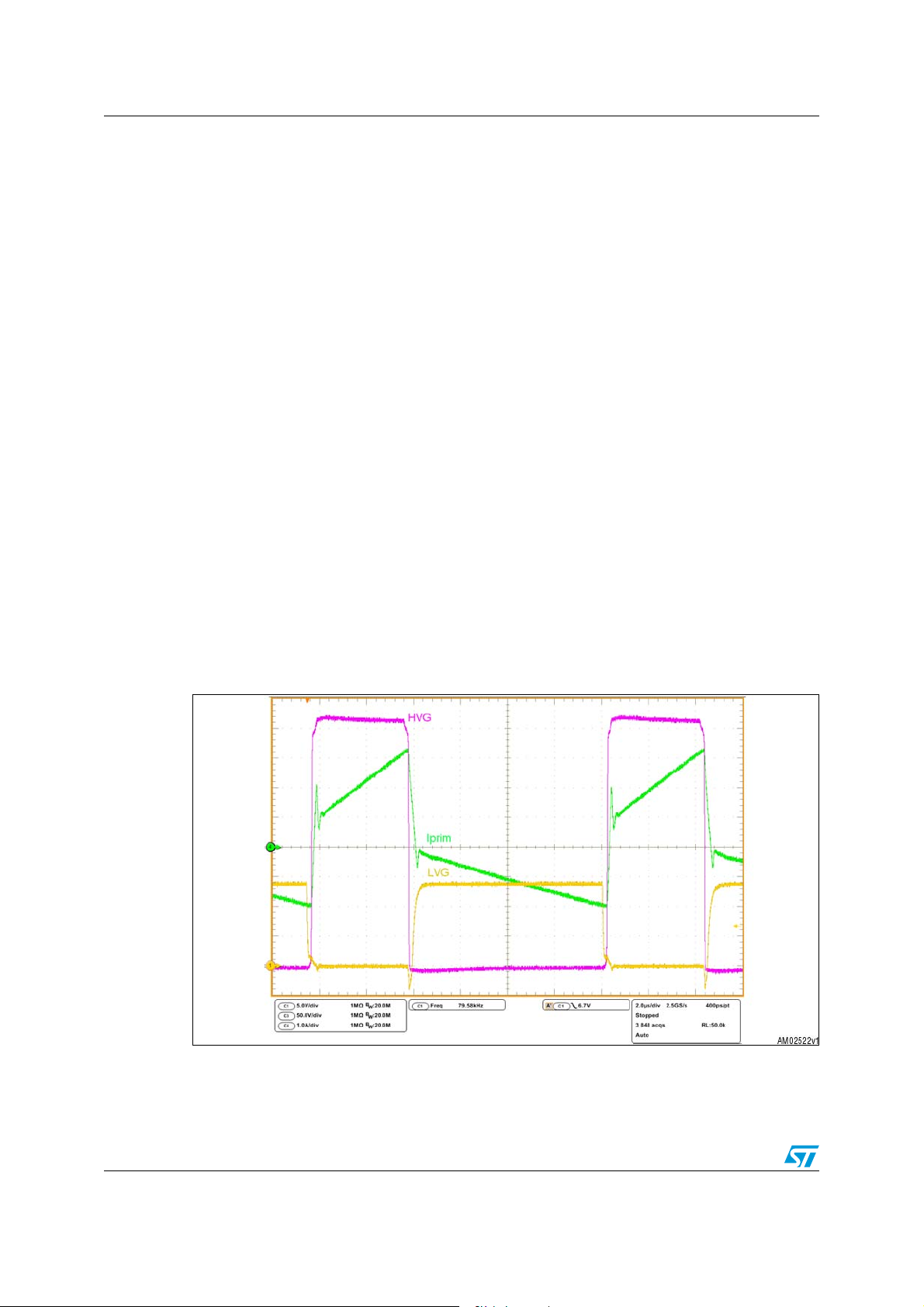
In Figure 6 the primary side key waveforms during steady-state operation with full load
applied are shown. Figure 7 shows the detail of the two transitions during one switching
cycle.
The AHB stage has been designed to operate at about 80 kHz with a nominal input voltage
of 400 V (PFC output bus). The transformer design is the result of a trade-off between the
half bridge MOSFETs zero voltage switching (ZVS) operation requirements, the primary rms
current, and duty cycle losses. In fact, ZVS can be achieved by reducing the magnetizing
inductance or increasing the leakage inductance. With the output power of this board, the
first solution implies having very high rms primary current which leads to high losses. The
second solution introduces the so called “duty cycle losses”. When the leakage inductance
is de-magnetizing, the voltages on the secondary side windings are zero and therefore the
output mean value is reduced with respect to the same half bridge duty cycle and negligible
leakage inductance. Duty cycle losses limit the hold-up capability of the power supply
because they increase the minimum input voltage that guarantees output regulation.
In this design the system works with ZVS for both MOSFETs at full load. Because of the
intrinsic asymmetry of the topology the behavior of the two switches is different. When the
load is reduced the low side MOSFET always operates in ZVS while the high side one starts
loosing ZVS. The high side MOSFET never turns on with full bus voltage applied between its
drain and source. As shown in Figure 8, even at 20 % of rated load the Vds at turn-on is
about 100 V, definitely lower compared with the 400 V of a hard switching solution.
This design can therefore meet both efficiency and dynamic requirements.
Figure 6. AHB primary side key waveforms @ full load
Ch1: LVG pin voltage (yellow)
Ch3: HVG pin voltage (purple)
Ch4: Primary winding current (green)
12/49 Doc ID 17402 Rev 2
Page 13
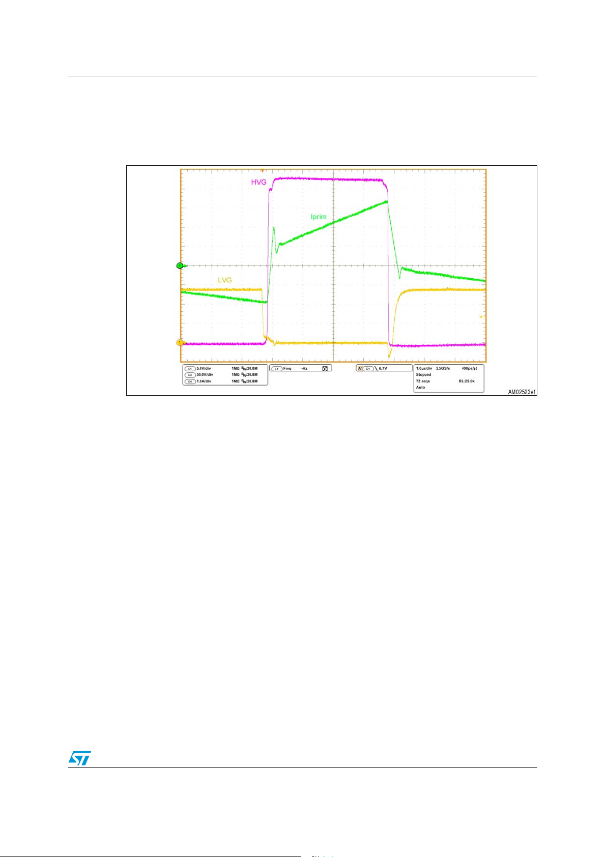
AN3203 Asymmetrical half bridge operation
The signal HVG is the sum of the half bridge node (FGND pin of L6591) and the high side
gate driver voltages. This peculiarity allows both waveforms and the ZVS operation for the
high side MOSFET to be checked. The driver activation is visible on the HVG signal when
there is a small voltage step on the high part of the waveform.
Figure 7. AHB zero voltage switching detail @ full load
Ch1: LVG pin voltage (yellow)
Ch3: HVG pin voltage (purple)
Ch4: Primary winding current (green)
Doc ID 17402 Rev 2 13/49
Page 14
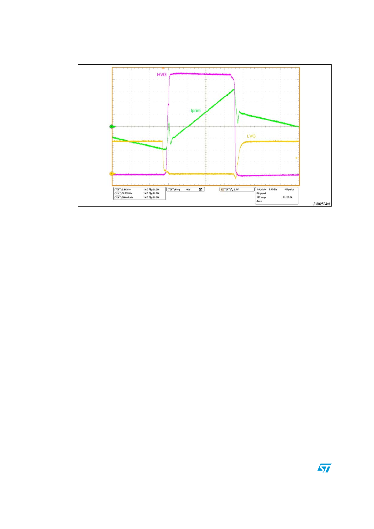
Asymmetrical half bridge operation AN3203
Figure 8. AHB transitions detail @ 20 % rated load
Ch1: LVG pin voltage (yellow)
Ch3: HVG pin voltage (purple)
Ch4: Primary winding current (green)
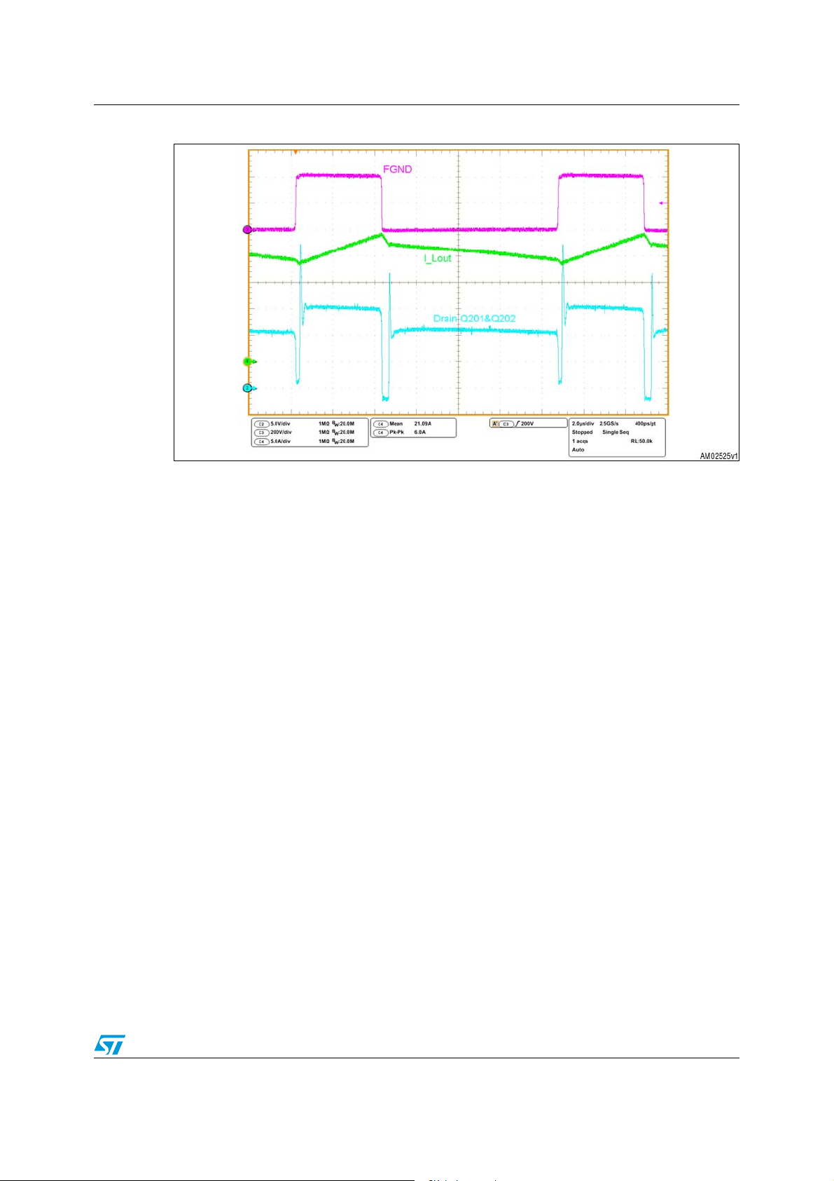
The key waveforms at the secondary side are shown in Figure 9. It is interesting to note that,
while the current is swapped between the two SR MOSFETs, the voltage at their drain is
nearly zero. The time required for current swap is directly proportional to the primary
leakage inductance. As mentioned before, the effect of this phenomenon is the duty cycle
losses.
14/49 Doc ID 17402 Rev 2
Page 15
AN3203 Asymmetrical half bridge operation
Figure 9. AHB secondary side key waveforms @ full load
Ch2: Q201 and Q202 drain pin (blue)
Ch3: FGND pin voltage (purple)
Ch4: Diode D13 current (green)
In order to improve the overall efficiency of the power supply, synchronous rectification has
been used. The two AHB output diodes have been replaced with two MOSFETs. A self
driven technique has been used to obtain a cheap solution. Two extra windings at the
secondary side generate the two square waves that, opportunely shifted, drive the two SR
MOSFETs gates directly. Referring to Q201, the extra winding (realized with just one turn)
starts from transformer pin 10 and ends in TON_DR_FLYWIRE. C210, D204, and R216 are
used to shift the voltage at the correct level to drive the MOSFET. R202 helps to keep the
MOSFET off if no driving signal is applied. A similar circuit drives the gate of Q202 starting
from the TOFF_DR_FLYWIRE signal.
Doc ID 17402 Rev 2 15/49
Page 16

Asymmetrical half bridge operation AN3203
2.2 Short-circuit protection
In case of a short-circuit at the AHB output the overload protection (OLP) is activated.
Figure 10 shows the pins involved in this function. When the short-circuit is applied, the
COMP pin saturates high. The IC detects this condition and starts charging the SS
capacitor. When the SS voltage reaches 5 V the system is shut down, when it reaches 6.4 V
the IC is latched. The PFC controller is also stopped: when the L6591 activates the
protection, the PFC_STOP signal pulls the L6563S RUN pin down to below the 0.8V
threshold. The latch is kept thanks to the auxiliary stage that remains active and provides
the VCC voltage.
In order to restart the system it is necessary to recycle the L6591 VCC voltage between the
UVLO thresholds. This can be done by removing the PS_ON signal in the auxiliary stage.
Figure 10. Short-circuit behavior detail
Ch1: SS pin voltage (yellow)
Ch2: COMP pin voltage (blue)
Ch3: FGND pin voltage, (purple)
Ch4: L6563S RUN pin voltage (green)
16/49 Doc ID 17402 Rev 2
Page 17

AN3203 Complete system
3 Complete system
3.1 Overvoltage protection
Every output is protected against overvoltage. The +12 V, +5 V and +3.3 V are monitored on
the auxiliary power supply schematic page. They use three Zener diodes to fix the three
overvoltage thresholds. In case one of the three voltages exceeds its threshold the latch
realized with Q604 and Q605 is turned on and the VCC for the L6591 and L6563S is
removed.
The two outputs +5 V and +3.3 V also have an overvoltage protection integrated into the
L6727 controller.
The +5 V_SB output is protected using the OVP protection of the VIPer27H that senses its
output voltage through the auxiliary winding. A threshold on the CONT pin detects the OVP
condition and stops the IC operation. This protection has an auto-restart behavior.
3.2 Load transients
The following figures show the behavior of the outputs during load transients. Each image
shows the transition from 20 % to 100 % of rated current and vice versa for a single output
voltage. The current slope is 0.5 A/µs for all the current variations.
Figure 11. Load transient on +12 V output
Doc ID 17402 Rev 2 17/49
Page 18

Complete system AN3203
Figure 12. Load transient on +5 V output
Figure 13. Load transient on +3.3 V output
3.3 Standby operation
When the PS_ON is not high, the system is in standby mode. Good performance is obtained
thanks to the VIPer27H high voltage converter. Efficiency and no-load consumption values
are shown in the next chapter.
18/49 Doc ID 17402 Rev 2
Page 19

AN3203 Electrical performance
4 Electrical performance
4.1 Efficiency measurement and no-load consumption
The efficiency measurements taken at the two nominal voltages are seen in the following
tables. The +5 V_SB output was unloaded during these measurements.
Table 1. Efficiency @ 115 Vrms
Load +12 V @load[A] +5 V @load[A] +3.3 V @load[A] Pout [W] Pin [W] Eff [%]
20 % 12.13 2.702 5.02 2.409 3.33 1.6 50.196 58.5 85.81 %
25 % 12.13 3.374 5.019 3.008 3.329 2.004 62.695 71.97 87.11 %
50 % 12.13 6.749 5.012 6.007 3.325 3.999 125.27 140.22 89.34 %
75 % 12.13 10.122 5.003 9.006 3.318 6.008 187.77 211.19 88.91 %
100 % 12.12 13.5 4.996 12.003 3.313 8.001 250.09 285.41 87.63 %
Table 2. Efficiency @ 230 Vrms
Load +12 V @load[A] +5 V @load[A] +3.3 V @load[A] Pout [W] Pin [W] Eff [%]
20 % 12.14 2.701 5.019 2.408 3.329 1.599 50.199 58.62 85.63 %
25 % 12.14 3.374 5.018 3.008 3.328 2.003 62.720 71.52 87.70 %
50 % 12.13 6.754 5.011 6.006 3.323 3.998 125.31 138.07 90.76 %
75 % 12.12 10.122 5.004 9.006 3.318 6.008 187.68 207.49 90.45 %
100 % 12.12 13.5 4.997 12.002 3.313 8.001 250.10 279.66 89.43 %
The 80 PLUS
®
program fixes several efficiency levels that describe how energy-efficient a
computer power supply is. The program defines the minimum efficiency requirements at 20
%, 50 %, 100 % of rated load and a minimum power factor requirement.
According to the program a power supply could be classified in 4 or 5 levels:
Table 3. 80 PLUS® program efficiency levels (115Vac)
Level Eff @ 20 % Eff @ 50 % Eff @ 100 % PF (@ load %)
80 PLUS > 80 % > 80 % > 80 % > 0.9 @ 100 %
80 PLUS Bronze > 82 % > 85 % > 82 % > 0.9 @ 50 %
80 PLUS Silver > 85 % > 88 % > 85 % > 0.9 @ 50 %
80 PLUS Gold > 87 % > 90 % > 87 % > 0.9 @ 50 %
80 PLUS Platinum > 90 % > 92 % > 89 % > 0.95 @ 50 %
Note: This table refers to power supplies for desktops, workstations, and non-redundant server
applications with 115 Vac mains
Doc ID 17402 Rev 2 19/49
Page 20

Electrical performance AN3203
®
Table 4. 80 PLUS
Level Eff @ 20% Eff @ 50% Eff @ 100% PF (@ load%)
80 PLUS Bronze > 81% > 85% > 81% > 0.9 @ 50%
80 PLUS Silver > 85% > 89% > 85% > 0.9 @ 50%
80 PLUS Gold > 88% > 92% > 88% > 0.9 @ 50%
80 PLUS Platinum > 90% > 94% > 91% > 0.95 @ 50%
program efficiency levels (230 Vac)
Note: This table refers to power supplies for redundant, data center applications with 230Vac
mains
This demonstration board is compliant with the 80 PLUS
please refer to Tab l e 9 ). Since this is basically a desktop PC power supply, the tests were
performed at 115 Vac. Certification report and other details can be found on the 80 PLUS
®
Silver specifications (for PF data
®
web site.
Similar levels of efficiency and power factor are defined also by the Climate Savers
Computing Initiative. According to the measurements carried out, the demonstration board
is compliant with “Climate Savers Computing Silver” level.
Table 5. Climate Savers Computing Initiative (for multi-output PSU)
Load
condition
20 % 82 % 0.8 85 % 0.8 87 % 0.8
50 % 85 % 0.9 88 % 0.9 90 % 0.9
100 % 82 % 0.95 85 % 0.95 87 % 0.95
Bronze Silver Gold
Efficiency PF Efficiency PF Efficiency PF
Ta bl e 6 shows the no-load consumption. These values are taken with the signal PS_ON
kept low, therefore only the auxiliary stage is active and only the +5 V_SB output is present.
The board showed very good values (below 200 mW over the whole input voltage range),
especially when considering that the inactive stages have a certain residual consumption
(only the voltage dividers in the input stage waste about 100 mW @ 230 Vac).
Table 6. No-load consumption
Vin [Vac] 90 115 135 180 230 264
Pin [mW] 59 70 82 113 161 199
Figure 14 and Figure 15 show the graph of the efficiency vs. output power at the two
nominal input voltages while Figure 16 shows the graph of the input power vs. input voltage
with no load applied. It is clearly visible that the power supply is compliant with the 80
®
PLUS
SILVER specification and it is very close to the GOLD one.
20/49 Doc ID 17402 Rev 2
Page 21

AN3203 Electrical performance
Figure 14. Efficiency vs. O/P power @ 115 Vac
Figure 15. Efficiency vs. O/P power @ 230 Vac
Figure 16. No-load consumption
Doc ID 17402 Rev 2 21/49
Page 22

Electrical performance AN3203
Some measurements with low output loads were also taken. They refer only to the operation
of the auxiliary stage, while the other stages are off. Results are shown in Table 7 and
Ta bl e 8 and plotted in Figure 17. The standby consumption allows the US Executive Order
13221 - “1-Watt Standby” to be met. To be more precise, when the output power is reduced
to 0.5 W, the input power is lower than 1 W (efficiency greater than 50 %). This is a very
common requirement for power supply manufacturers.
Table 7. Low load efficiency @ 115 Vrms
Vout [V] Iout [A] Pout [W] Pin [W] Eff [%]
4.993 0.1 0.499 0.688 72.6 %
4.993 0.2003 1.000 1.312 76.2 %
4.993 0.3007 1.501 1.933 77.7 %
4.993 0.3996 1.995 2.544 78.4 %
4.993 0.5 2.497 3.163 78.9 %
4.993 0.6002 2.997 3.812 78.6 %
4.993 0.7006 3.498 4.501 77.7 %
4.993 0.7994 3.991 5.114 78.0 %
4.993 0.8998 4.493 5.664 79.3 %
4.993 1.0001 4.993 6.209 80.4 %
Table 8. Low load efficiency @ 230 Vrms
Vout [V] Iout [A] Pout [W] Pin [W] Eff [%]
4.994 0.1 0.499 0.826 60.5 %
4.994 0.2002 1.000 1.471 68.0 %
4.994 0.3006 1.501 2.13 70.5 %
4.994 0.3995 1.995 2.798 71.3 %
4.994 0.4999 2.497 3.486 71.6 %
4.994 0.6001 2.997 4.161 72.0 %
4.994 0.7006 3.499 4.806 72.8 %
4.994 0.7994 3.992 5.304 75.3 %
4.994 0.8997 4.493 5.934 75.7 %
4.994 1 4.994 6.667 74.9 %
22/49 Doc ID 17402 Rev 2
Page 23

AN3203 Electrical performance
Figure 17. Efficiency at low loads
Low load eciency (AUX only)
85.0%
80.0%
75.0%
70.0%
65.0%
60.0%
55.0%
50.0%
0.0 1.0 2.0 3.0 4.0 5.0
115Vac
230Vac
Output power [W]
Doc ID 17402 Rev 2 23/49
Page 24

Electrical performance AN3203
4.2 Thermal considerations
This demonstration board has been designed for operation with forced air cooling, very
common in ATX power supply applications. As the component temperatures depend on the
type of fan used and on the airflow path inside the board housing, a thermal map of the
board isn’t significant and has not been taken. When the system works at 25 °C with full
load and no forced air, temperatures are not so high. If a heatsink with lower thermal
resistance for MOSFETs Q201 and Q202 is used, fanless operation may be achieved. For
example, the same shape of the heatsink used for D1, Q1, Q2, D3, Q101, and Q102 could
be used for fanless operation. A picture of this application is shown in Figure 18.
Figure 18. Fanless board
24/49 Doc ID 17402 Rev 2
Page 25

AN3203 Electrical performance
4.3 Harmonic content measurement
The front-end PFC stage provides the reduction of the mains harmonic, allowing European
EN61000-3-2 and Japanese JEITA–MITI standards for class D equipment to be met.
Figure 19 shows the harmonic contents of the mains current at full load.
A measurement has also been taken with a 75 W input power which is the lowest limit for
using harmonic reduction techniques.
Figure 19. EN61000-3-2 and JEITA-MITI measurements @ full load
Figure 20. EN61000-3-2 and JEITA-MITI measurements @ 75 W in
To evaluate the performance of the PFC stage the PF and THD vs. input voltage graphs are
also shown, in Figure 21 and Figure 22, at full load and 75 W input power load conditions.
Ta bl e 9 shows the PF values at the three different load amounts defined in the 80 PLUS
and climate savers computing requirements.
®
Doc ID 17402 Rev 2 25/49
Page 26

Electrical performance AN3203
Vin [Vrms]
Figure 21. PF vs. input voltage
1.000
0.975
0.950
0.925
0.900
PF
0.875
0.850
0.825
0.800
80
Figure 22. THD vs. input voltage
20.00
18.00
16.00
14.00
12.00
10.00
THD [%]
8.00
6.00
4.00
2.00
0.00
80
250W out 75W in
120
120
160 200
250W out 75W in
160
Vin [Vrms]
200
240
280
AM02539v1
240
280
AM02540v1
Table 9. PF vs. load
Load 115 Vac 230 Vac
20 % 0.972 0.857
50 % 0.984 0.954
100 % 0.992 0.981
26/49 Doc ID 17402 Rev 2
Page 27

AN3203 Electrical performance
4.4 Single output configuration
The power supply overall efficiency is given by the product of the efficiency of each stage. It
is interesting to take a look at the efficiency of the single +12 V output system. Such power
supply can be obtained from the complete system just removing the two daughter boards
that realize the DC-DC post regulation. The single output system can manage the same
power of the multi-output board, hence it is capable of sourcing about 21 A from the +12 V
output.
The system is now made up of input filter, PFC stage, AHB stage and Stand-by stage. The
latter is left unloaded for the following efficiency measurements:
Table 10. Single output efficiency @ 115 Vac
Load [%] Iout [A] Vout [V] Pout [W] Pin [W] Eff [%]
10 % 2.085 12.06 25.145 29.79 84.41%
20 % 4.17 12.06 50.290 56.27 89.37%
25 % 5.205 12.06 62.772 69.63 90.15%
50 % 10.421 12.05 125.573 137.4 91.39%
75 % 15.623 12.04 188.101 207.4 90.69%
100 % 20.829 12.03 250.573 279.8 89.55%
Table 11. Single output efficiency @ 230 Vac
Load [%] Iout [A] Vout [V] Pout [W] Pin [W] Eff [%]
10 % 2.084 12.06 25.133 31.02 81.02%
20 % 4.169 12.06 50.278 56.65 88.75%
25 % 5.204 12.06 62.760 69.39 90.45%
50 % 10.421 12.05 125.573 135.3 92.81%
75 % 15.622 12.04 188.089 203.9 92.25%
100 % 20.827 12.03 250.549 274.2 91.37%
It is interesting to compare the result obtained with the single output configuration with the
80 PLUS
®
levels (see Table 3 and Tab l e 4 ). The comparison is graphically shown in
Figure 23 and Figure 24.
Doc ID 17402 Rev 2 27/49
Page 28

Electrical performance AN3203
Figure 23. Single output efficiency @ 115 Vac
Figure 24. Single output efficiency @ 230 Vac
From the pictures it is immediately clear that the single output configuration is over
performing the 80 PLUS
®
GOLD efficiency targets and that it is close to the PLATINUM
ones.
Such performance has been achieved mainly thanks to the AHB stage, which is very
efficient. In Ta bl e 1 2 and Figure 25 efficiency data for the AHB stage only are given. These
measurements were taken by supplying the stage with a 400Vdc input voltage and with the
auxiliary operating without load.
28/49 Doc ID 17402 Rev 2
Page 29

AN3203 Electrical performance
Table 12. AHB efficiency with 400 Vdc input
Load [%] Iout [A] Vout [V] Pout [W] Pin [W] Eff [%]
10 % 2.078 12.06 25.061 28.61 87.59%
20 % 4.163 12.06 50.206 53.79 93.34%
25 % 5.213 12.06 62.869 66.6 94.40%
50 % 10.415 12.05 125.501 131.3 95.58%
75 % 15.616 12.04 188.017 197.9 95.01%
100 % 20.823 12.03 250.501 266.3 94.07%
Figure 25. AHB stage only efficiency (Vin = 400 Vdc)
When looking at these efficiency results we have also to keep in mind that the AHB stage is
a cost effective solution, thanks to a low count of components needed, no need of a
controller IC for the synchronous rectification and a small output choke.
Doc ID 17402 Rev 2 29/49
Page 30

Conducted noise measurements (pre-compliance test) AN3203
5 Conducted noise measurements (pre-compliance
test)
Figure 26, 27, 28, and 29 show the conducted noise measurements with peak and average
detection taken at both nominal voltages. All the measurements are performed with full load
output and only consider the worst phase. The average measurements show good margins
with respect to the mask limit (which is the EN55022 CLASS B).
Figure 26. CE peak measurement@115 Vac and full load
Figure 27. CE peak measurement @ 230 Vac and full load
30/49 Doc ID 17402 Rev 2
Page 31

AN3203 Conducted noise measurements (pre-compliance test)
Figure 28. CE average measurement@115 Vac and full load
Figure 29. CE average measurement@230 Vac and full load
Doc ID 17402 Rev 2 31/49
Page 32

Parts list AN3203
6 Parts list
Table 13. EVL250W-ATX80PL bill of materials
Ref Value Description Manufacturer
C1 220 µF Electrolytic capacitor VXG – 450 V Rubycon
C2 100 nF Polypropylene capacitor 450 V
C3 1.0 µF Polypropylene capacitor 450 V – ECWF2W105JA Panasonic
C4 1 µF SMD ceramic capacitor X7R – 16 V AVX
C5 22 µF Electrolytic capacitor 25 V – 105 °C
C6 0.1 µF SMD ceramic capacitor X7R – 25 V AVX
C7 3.3 nF SMD ceramic capacitor X7R – 50 V AVX
C8 2.2 nF SMD ceramic capacitor X7R – 50 V AVX
C9 560 pF SMD ceramic capacitor NP0 – 50 V AVX
C10 330 pF SMD ceramic capacitor NP0 – 50 V AVX
C11 470 pF SMD ceramic capacitor X7R – 50 V AVX
C12 220 nF SMD ceramic capacitor X7R – 25 V AVX
C13 1 nF SMD ceramic capacitor X7R – 50 V AVX
C14 33 nF SMD ceramic capacitor X7R – 25 V AVX
C15 10 nF SMD ceramic capacitor X7R – 25 V AVX
C101 1.0 µF Polypropylene capacitor 450 V – ECWF2W105JA Panasonic
C102 0.1 µF SMD ceramic capacitor X7R – 25 V AVX
C103 22 µF Electrolytic capacitor 25 V – 105 °C
C104 10 nF SMD ceramic capacitor X7R – 25 V AVX
C105 0.1 µF SMD ceramic capacitor X7R – 25 V AVX
C106 220 pF SMD ceramic capacitor NP0 – 50 V 1 % AVX
C107 10 nF SMD ceramic capacitor X7R – 25 V AVX
C108 470 nF SMD ceramic capacitor X7R – 16 V AVX
C109 0.1 µF SMD ceramic capacitor X7R – 25 V AVX
C110 100 pF SMD ceramic capacitor NP0 – 50 V AVX
C112 10 nF SMD ceramic capacitor X7R – 50 V AVX
C201 1500 µF Electrolytic capacitor HM – 16 V Nichicon
C202 1500 µF Electrolytic capacitor HM – 16 V Nichicon
C203 4.7 nF SMD ceramic capacitor X7R – 50 V AVX
C204 3.3 nF SMD ceramic capacitor X7R – 100 V AVX
C205 220 nF SMD ceramic capacitor X7R – 25 V AVX
C206 0.1 µF SMD ceramic capacitor X7R – 25 V AVX
32/49 Doc ID 17402 Rev 2
Page 33

AN3203 Parts list
Table 13. EVL250W-ATX80PL bill of materials (continued)
Ref Value Description Manufacturer
C207 470 µF Electrolytic capacitor ZLH – 16 V Rubycon
C208 0.1 µF SMD ceramic capacitor X7R – 25 V AVX
C209 2.2 µF SMD ceramic capacitor X7R – 25 V AVX
C210 2.2 µF SMD ceramic capacitor X7R – 25 V AVX
C301 1500 µF Electrolytic capacitor HM – 16 V Nichicon
C302 1500 µF Electrolytic capacitor HM – 16 V Nichicon
C303 1500 µF Electrolytic capacitor HM – 16 V Nichicon
C304 1.2 nF SMD ceramic capacitor X7R – 50 V AVX
C305 0.1 µF SMD ceramic capacitor X7R – 25 V AVX
C306 4.7 µF SMD ceramic capacitor X7R – 16 V AVX
C307 0.1 µF SMD ceramic capacitor X7R – 25 V AVX
C308 1 nF SMD ceramic capacitor X7R – 50 V AVX
C309 10 nF SMD ceramic capacitor X7R – 25 V AVX
C310 2.2 nF SMD ceramic capacitor X7R – 50 V AVX
C311 100 µF SMD ceramic cap 6.3 V – GRM32EF50J107ZE20K Murata
C312 100 µF SMD ceramic cap 6.3 V – GRM32EF50J107ZE20K Murata
C313 10 µF SMD ceramic capacitor X7R – 6.3 V AVX
C501 1500 µF Electrolytic capacitor HM – 16 V Nichicon
C502 1500 µF Electrolytic capacitor HM – 16 V Nichicon
C503 1500 µF Electrolytic capacitor HM – 16 V Nichicon
C504 1.2 nF SMD ceramic capacitor X7R – 50 V AVX
C505 4.7 µF SMD ceramic capacitor X7R – 16 V AVX
C506 0.1 µF SMD ceramic capacitor X7R – 25 V AVX
C507 0.1 µF SMD ceramic capacitor X7R – 25 V AVX
C508 10 nF SMD ceramic capacitor X7R – 25 V AVX
C509 1 nF SMD ceramic capacitor X7R – 50 V AVX
C510 2.2 nF SMD ceramic capacitor X7R – 50 V AVX
C511 100 µF SMD ceramic cap 6.3 V – GRM32EF50J107ZE20K Murata
C512 100 µF SMD ceramic cap 6.3 V – GRM32EF50J107ZE20K Murata
C513 10 µF SMD ceramic capacitor X7R – 10 V AVX
C602 470 pF Ceramic capacitor – 1 kV
C603 1500 µF Electrolytic capacitor HM – 16 V Nichicon
C604 470 µF Electrolytic capacitor ZLH – 16 V Rubycon
C605 10 µF Electrolytic capacitor 50V – 105 °C
C606 47 µF Electrolytic capacitor 35V – 105 °C
Doc ID 17402 Rev 2 33/49
Page 34

Parts list AN3203
Table 13. EVL250W-ATX80PL bill of materials (continued)
Ref Value Description Manufacturer
C607 0.1 µF SMD ceramic capacitor X7R – 25 V AVX
C608 10 nF SMD ceramic capacitor X7R – 25 V AVX
C609 0.1 µF SMD ceramic capacitor X7R – 25 V AVX
C611 220 nF SMD ceramic capacitor X7R – 25 V AVX
C612 47 nF SMD ceramic capacitor X7R – 25 V AVX
C613 10 nF SMD ceramic capacitor X7R – 25 V AVX
C614 0.1 µF SMD ceramic capacitor X7R – 25 V AVX
C615 10 nF SMD ceramic capacitor X7R – 25 V AVX
CN1 AC INLET 3.96 mm pitch KK series Molex
CX1 470 nF Polypropylene X2 capacitor R46 – 275 Vac Arcotronics
CX3 680 nF Polypropylene X2 capacitor R46 – 275 Vac Arcotronics
CY1 2N2 Ceramic Y1 capacitor – DE1E3KX222M Murata
CY2 2N2 Ceramic Y1 capacitor – DE1E3KX222M Murata
CY3 4N7 Ceramic Y1 capacitor – DE1E3KX472M Murata
D1 D15XB60 15A/600V bridge rectifier Shindengen
D2 1N5406 3A/600V rectifier
D3 STPSC1006D 10A/600V silicon carbide Schottky rectifier STMicroelectronics
D4 1N4148WS Fast switching diode
D5 1N4148WS Fast switching diode
D6 1N4148 Fast switching diode
D101 LL4148 Fast switching diode
D102 LL4148 Fast switching diode
D103 STTH1L06 1A/600V ultrafast high voltage rectifier STMicroelectronics
D203 LL4148 Fast switching diode
D204 LL4148 Fast switching diode
D301 TMMBAT43 Small signal Schottky diode STMicroelectronics
D501 TMMBAT43 Small signal Schottky diode STMicroelectronics
D601 STTH102A 1A/200V high efficiency ultrafast diode STMicroelectronics
D602 BAV103 Switching diode
D603 BAV103 Switching diode
D604 STTH108A 1A/800V high voltage ultrafast rectifier STMicroelectronics
D605 STPS5L60 5A/60V power Schottky diode STMicroelectronics
D606 BAT48 Small signal Schottky diode STMicroelectronics
D607 LL4148 Fast switching diode
D608 LL4148 Fast switching diode
34/49 Doc ID 17402 Rev 2
Page 35

AN3203 Parts list
Table 13. EVL250W-ATX80PL bill of materials (continued)
Ref Value Description Manufacturer
D609 LL4148 Fast switching diode
F1 FUSE - 10A Fuse T10A – time delay
IC1 L6563S Enhanced transition-mode PFC controller STMicroelectronics
IC2 L6591 PWM controller for ZVS half bridge STMicroelectronics
IC3 VIPER27HN Offline high voltage converters STMicroelectronics
IC200 TL431AIZ Programmable voltage reference STMicroelectronics
IC300 L6727 Single phase PWM controller STMicroelectronics
IC500 L6727 Single phase PWM controller STMicroelectronics
IC600 TS431AIZ Low voltage adjustable shunt reference STMicroelectronics
L1 2x4 mH Common mode choke 1606.0010 Magnetica
L2 2xJUMPER
L3 60 µH Differential mode choke 1119.0013 Magnetica
L4 870 µH PFC choke
L5 0.75 µH AHB post filter inductor 1019.0016 Magnetica
L201 3.7 µH AHB output choke 2029.0002 Magnetica
L301 3.7 µH DC-DC choke 2029.0001 Magnetica
L501 3.7 µH DC-DC choke 2029.0001 Magnetica
L601 2.7 µH AUX stage post filter inductor 1048.0010 Magnetica
NTR1 2R5 NTC inrush current limiter B57237S0259M000 EPCOS
OPTO1 PC817A Optocoupler SHARP
OPTO2 PC817A Optocoupler SHARP
OPTO3 PC817A Optocoupler SHARP
Q1 STF12NM50N 500 V MDmesh II Power MOSFET STMicroelectronics
Q2 STF12NM50N 500 V MDmesh II Power MOSFET STMicroelectronics
Q3 BC857C PNP small signal BJT
Q101 STF21NM50N 500 V MDmesh™ II Power MOSFET STMicroelectronics
Q102 STF21NM50N 500 V MDmesh™ II Power MOSFET STMicroelectronics
Q201 STP120NF04 40 V STripFET™ II Power MOSFET STMicroelectronics
Q202 STP75NF75FP 75 V STripFET™ II Power MOSFET STMicroelectronics
Q301 STD95N2LH5 25 V STripFET™ V Power MOSFET STMicroelectronics
Q302 STD95N2LH5 25 V STripFET™ V Power MOSFET STMicroelectronics
Q303 STD95N2LH5 25 V STripFET™ V Power MOSFET STMicroelectronics
Q501 STD95N2LH5 25 V STripFET™ V Power MOSFET STMicroelectronics
Q502 STD95N2LH5 25V STripFET™ V Power MOSFET STMicroelectronics
Q503 STD95N2LH5 25 V STripFET™ V Power MOSFET STMicroelectronics
Doc ID 17402 Rev 2 35/49
Page 36

Parts list AN3203
Table 13. EVL250W-ATX80PL bill of materials (continued)
Ref Value Description Manufacturer
Q601 MMBT3904 NPN small signal BJT
Q603 MMBT3904 NPN small signal BJT
Q604 MMBT3904 NPN small signal BJT
Q605 MMBT3906 PNP small signal BJT
R1 0R33 Metal film resistor – 5 % – 250 ppm/°C – 2 W
R2 0R33 Metal film resistor – 5 % – 250 ppm/°C – 2 W
R3 6.8 R SMD film resistor – 5 % – 250 ppm/°C – 0805
R4 6.8 R SMD film resistor – 5 % – 250 ppm/°C – 0805
R5 47 K SMD film resistor – 5 % – 250 ppm/°C – 0603
R6 47 K SMD film resistor – 5 % – 250 ppm/°C – 0603
R7 10 R SMD film resistor – 5 % – 250 ppm/°C – 0603
R8 2.2 Meg SMD film resistor – 1 % – 100 ppm/°C – 1206
R9 2.2 Meg SMD film resistor – 1 % – 100 ppm/°C – 1206
R10 2.2 Meg SMD film resistor – 1 % – 100 ppm/°C – 1206
R11 51 K SMD film resistor – 1 % – 100 ppm/°C – 0603
R12 1 Meg SMD film resistor – 1 % – 100 ppm/°C – 0603
R13 2.4 K Metal film resistor – 1% – 100 ppm/°C – 0.16 W
R14 6.8 K SMD film resistor – 1 % – 100 ppm/°C – 0603
R15 2.4 K SMD film resistor – 1 % – 100 ppm/°C – 0603
R16 220 K SMD film resistor – 1 % – 100 ppm/°C – 0603
R17 1.5 Meg SMD film resistor – 1 % – 100 ppm/°C – 1206
R18 1.5 Meg SMD film resistor – 1 % – 100 ppm/°C – 1206
R19 1.5 Meg SMD film resistor – 1 % – 100 ppm/°C – 1206
R20 1.6 Meg SMD film resistor – 1 % – 100 ppm/°C – 1206
R21 1.6 Meg SMD film resistor – 1% – 100 ppm/°C – 1206
R22 1.6 Meg SMD film resistor – 1 % – 100 ppm/°C – 1206
R23 470 R SMD film resistor – 5 % – 250 ppm/°C – 0603
R24 56 K SMD film resistor – 1 % – 100 ppm/°C – 0603
R25 56 K SMD film resistor – 1 % – 100 ppm/°C – 0603
R26 24 K SMD film resistor – 1 % – 100 ppm/°C – 0603
R28 56 K SMD film resistor – 1 % – 100 ppm/°C – 0603
R29 3.3 K SMD film resistor – 1 % – 100 ppm/°C – 0603
R30 2.7 K SMD film resistor – 1 % – 100 ppm/°C – 0603
R31 3.3 R SMD film resistor – 5 % – 250 ppm/°C – 0805
R32 3.3 R SMD film resistor – 5 % – 250 ppm/°C – 0805
36/49 Doc ID 17402 Rev 2
Page 37

AN3203 Parts list
Table 13. EVL250W-ATX80PL bill of materials (continued)
Ref Value Description Manufacturer
R101 0.18 R Metal film resistor – 5 % – 250 ppm/°C – 2 W
R103 10 R SMD film resistor – 5 % – 250 ppm/°C – 0603
R104 4.7 K SMD film resistor – 5 % – 250 ppm/°C – 0603
R105 100 K SMD film resistor – 5 % – 250 ppm/°C – 0603
R107 20 K SMD film resistor – 1 % – 100 ppm/°C – 0603
R108 36 K SMD film resistor – 1 % – 100 ppm/°C – 0603
R109 20 R SMD film resistor – 5 % – 250 ppm/°C – 0805
R110 47 K SMD film resistor – 5 % – 250 ppm/°C – 0603
R111 20 R SMD film resistor – 5 % – 250 ppm/°C – 0805
R112 47 K SMD film resistor – 5 % – 250 ppm/°C – 0603
R113 1 K Metal film resistor – 1 % – 100 ppm/°C – 0.16 W
R114 2.2 R SMD film resistor – 5 % – 250 ppm/°C – 0603
R115 2.2 R SMD film resistor – 5 % – 250 ppm/°C – 0603
R116 100 K SMD film resistor – 5 % – 250 ppm/°C – 0603
R201 2.2 R SMD film resistor – 5 % – 250 ppm/°C – 0805
R202 15 K SMD film resistor – 5 % – 250 ppm/°C – 0805
R203 13 R Metal film resistor – 5 % – 250 ppm/°C – 2 W
R204 5.6 R Metal film resistor – 5 % – 250 ppm/°C – 2 W
R206 2.2 R SMD film resistor – 5 % – 250 ppm/°C – 0805
R208 15 K SMD film resistor – 5 % – 250 ppm/°C – 0805
R209 1 K SMD film resistor – 1 % – 100 ppm/°C – 0603
R210 2.2 K SMD film resistor – 1 % – 100 ppm/°C – 0603
R211 20 K SMD film resistor – 1 % – 100 ppm/°C – 0603
R212 10 K SMD film resistor – 1 % – 100 ppm/°C – 0603
R213 5.6 K SMD film resistor – 1 % – 100 ppm/°C – 0603
R214 75 K SMD film resistor – 1 % – 100 ppm/°C – 0603
R215 6.8 K SMD film resistor – 5 % – 250 ppm/°C – SOD-80
R216 10 K SMD film resistor – 5 % – 250 ppm/°C – SOD-80
R301 22 R SMD film resistor – 5 % – 250 ppm/°C – 0805
R302 22 R SMD film resistor – 5 % – 250 ppm/°C – 0805
R303 22 R SMD film resistor – 5 % – 250 ppm/°C – 0805
R304 22 R SMD film resistor – 5 % – 250 ppm/°C – 0805
R305 47 K SMD film resistor – 5 % – 250 ppm/°C – 0603
R306 47 K SMD film resistor – 5 % – 250 ppm/°C – 0603
R307 10 R SMD film resistor – 5 % – 250 ppm/°C – 0603
Doc ID 17402 Rev 2 37/49
Page 38

Parts list AN3203
Table 13. EVL250W-ATX80PL bill of materials (continued)
Ref Value Description Manufacturer
R308 10 R SMD film resistor – 5 % – 250 ppm/°C – 0603
R309 7.5 K SMD film resistor – 1 % – 100 ppm/°C – 0603
R310 6.34 K SMD film resistor – 1 % – 100 ppm/°C – 0603
R311 10 K SMD film resistor – 1 % – 100 ppm/°C – 0603
R312 2 K SMD film resistor – 1 % – 100 ppm/°C – 0603
R313 0 R SMD film resistor – 0603
R314 0 R SMD film resistor – 0805
R501 22 R SMD film resistor – 5 % – 250 ppm/°C – 0805
R502 22 R SMD film resistor – 5 % – 250 ppm/°C – 0805
R503 22 R SMD film resistor – 5 % – 250 ppm/°C – 0805
R504 22 R SMD film resistor – 5 % – 250 ppm/°C – 0805
R505 47 K SMD film resistor – 5 % – 250 ppm/°C – 0603
R506 47 K SMD film resistor – 5 % – 250 ppm/°C – 0603
R507 10 R SMD film resistor – 5 % – 250 ppm/°C – 0603
R508 10 R SMD film resistor – 5 % – 250 ppm/°C – 0603
R509 7.5 K SMD film resistor – 1 % – 100 ppm/°C – 0603
R510 10 K SMD film resistor – 1 % – 100 ppm/°C – 0603
R511 12.7 K SMD film resistor – 1 % – 100 ppm/°C – 0603
R512 2.4 K SMD film resistor – 1 % – 100 ppm/°C – 0603
R513 0 R SMD film resistor – 0603
R514 0 R SMD film resistor – 0805
R601 470 K SMD film resistor – 5 % – 250 ppm/°C – 1206
R602 4.7 R SMD film resistor – 5 % – 250 ppm/°C – 0805
R603 15 R SMD film resistor – 5 % – 250 ppm/°C – 0805
R604 56 K SMD film resistor – 1 % – 100 ppm/°C – 0603
R605 13 K SMD film resistor – 1 % – 100 ppm/°C – 0603
R606 10 R SMD film resistor – 5 % – 250 ppm/°C – 0805
R607 150 K SMD film resistor – 1 % – 100 ppm/°C – 0603
R610 1 K SMD film resistor – 1 % – 100 ppm/°C – 0603
R611 15 K SMD film resistor – 5 % – 250 ppm/°C – 0603
R612 10 K SMD film resistor – 1 % – 100 ppm/°C – 0603
R613 4.7 K SMD film resistor – 1 % – 100 ppm/°C – 0603
R614 47 K SMD film resistor – 1 % – 100 ppm/°C – 0603
R615 1.6 K SMD film resistor – 1 % – 100 ppm/°C – 0603
R616 1 K SMD film resistor – 1 % – 100 ppm/°C – 0603
38/49 Doc ID 17402 Rev 2
Page 39

AN3203 Parts list
Table 13. EVL250W-ATX80PL bill of materials (continued)
Ref Value Description Manufacturer
R617 1 K SMD film resistor – 1 % – 100 ppm/°C – 0603
R618 1.5 K SMD film resistor – 1 % – 100 ppm/°C – 0603
R619 10 K SMD film resistor – 1 % – 100 ppm/°C – 0603
R620 470 R SMD film resistor – 1 % – 100 ppm/°C – 0603
R621 1 K SMD film resistor – 1 % – 100 ppm/°C – 0603
R622 470 R SMD film resistor – 1 % – 100 ppm/°C – 0603
R623 100 R SMD film resistor – 1 % – 100 ppm/°C – 0603
R624 0 R SMD film resistor – 0603
R626 1 K SMD film resistor – 5 % – 250 ppm/°C – 0603
R627 1.5 K SMD film resistor – 5 % – 250 ppm/°C – 0805
R628 200 R SMD film resistor – 5 % – 250 ppm/°C – 0805
RX1 680 K SMD film resistor – 5 % – 250 ppm/°C – 1206
RX2 680 K SMD film resistor – 5 % – 250 ppm/°C – 1206
T1 Transformer AHB transformer 1965.0003 Magnetica
T2 Transformer AUX transformer 1031.0010 Magnetica
VDR1 Varistor 300 Vac – S14K300 – B72214S0301K101 EPCOS
ZD601 BZV55-B18 SMD Zener diode 18 V – 2 %
ZD603 BZX55B5V1 Zener diode 5V1 – 2 %
ZD604 BZX55-B13 Zener diode 13 V – 2 %
ZD605 BZX55B2V7 Zener diode 2V7 – 2 %
ZD606 BZV55-B36 SMD Zener diode 36 V – 2 %
Doc ID 17402 Rev 2 39/49
Page 40

PFC coil specification AN3203
7 PFC coil specification
● Application type: Consumer, IT
● Transformer type: Toroidal
● Coil former: none
● Max. temp. rise: 45 °C
● Max. operating ambient temp.: 60 °C
7.1 Electrical characteristics
● Converter topology: Boost, Fixed Off Time
● Core type: Dong Bu H106-093A
● Min. operating frequency: 20 kHz
● Primary inductance: 870 µH ±15 % @1 kHz - 0.25 V
● Max peak current: 5.3 A
●
Max RMS current: 3.37 A
Figure 30. Electrical diagram
pk
RMS
Table 14. Winding characteristics
Pins RMS current Nr. of turns Wire type
1 – 2 3.37 A
RMS
100.5 Ø 1.0mm – G2
Figure 31. Mechanical drawing (unit: mm)
40/49 Doc ID 17402 Rev 2
Page 41

AN3203 AHB transformer specification
8 AHB transformer specification
● Application type: Consumer, IT
● Transformer type: Open
● Coil former: vertical type, 6+6 pins
● Max. temp. rise: 45 °C
● Max. operating ambient temp.: 60 °C
● Mains insulation: Compliance with EN60950
8.1 Electrical characteristics
● Converter topology: Asymmetrical half bridge
● Core Type: PQ3230 – PC44 or equivalent
● Operating frequency: 80 kHz
(b)
(a)
● Primary inductance: 500 μH ±10 % @1 kHz – 0.25 V
● Air gap: 0.3 mm on central leg
● Leakage inductance: 12 μH typ. @100 kHz – 0.25 V
RMS
(c)
pk
● Primary capacitance: 6 pF typ.
● Max. peak primary current: 3.85 A
●
RMS primary current: 2 A
Figure 32. Electrical diagram
a. Measured between pins 2-4
b. Measured between pins 2-4 with secondaries and auxiliary windings shorted
c. Calculated considering primary inductance and resonance frequency
Doc ID 17402 Rev 2 41/49
Page 42

AHB transformer specification AN3203
3mm
Table 15. Winding characteristics
Pins Winding Current Nr. of turns Wire type
4 – 3 Primary 2.1 A
9,10 – 7,8 Secondary 1 15 A
7,8 – 11,12 Secondary 2 19.7 A
TonFW – 9,10 Sec.1 AUX 0.1 A
11,12 – ToffFW Sec.2 AUX 0.1 A
Note: Cover wire ends with silicon/teflon tube:
Use red tube for Ton-DR-Flyingwire
Use white tube for Toff-DR-Flyingwire
Figure 33. Windings position
SEC. AUX 1 & 2
SECONDARY 2
COIL FORMER
SECONDARY 1
RMS
RMS
RMS
RMS
RMS
PRIMARY
34
2 Copper foil 0.2 x 17 mm
3 Copper foil 0.2 x 17 mm
1 Ø 0.15 mm – G2
1 Ø 0.15 mm – G2
TIW – 2 x Ø0.4 mm
4 layers
INSULATING
TAPE
8.2 Mechanical aspect and pin numbering
● Maximum height from PCB: 33 mm
● Coil former type: vertical, 6+6 pins
● Pin distance: 5.08 mm
● Row distance: 30.5 mm
● Pin removed: # 5
● Manufacturer: Magnetica
● P/N: 1754.0004
3mm
42/49 Doc ID 17402 Rev 2
Page 43

AN3203 AHB transformer specification
Figure 34. Bottom view
Doc ID 17402 Rev 2 43/49
Page 44

AUX flyback transformer specification AN3203
9 AUX flyback transformer specification
● Application type: Consumer, IT
● Transformer type: Open
● Coil former: vertical type, 5+5 pins
● Max. temp. rise: 45 °C
● Max. operating ambient temp.: 60 °C
● Mains insulation: Compliance with EN60950
9.1 Electrical characteristics
● Converter topology: Flyback, CCM/DCM mode
● Core Type: E20/10/6 (EF20) - N87 or equivalent
● Operating frequency: 115 kHz
● Primary inductance: 1.7 mH 10 % @1 kHz - 0.25 V
Air gap: 1.24 mm on central leg
●
● Leakage inductance: 50 µH max. @100 kHz - 0.25 V
Max. peak primary current: 0.74 A
●
●
RMS primary current: 0.17 A
pk
RMS
(d)
(e)
Figure 35. Electrical diagram
d. Measured between pins 1-3
e. Measured between pins 1-3 with secondaries and auxiliary windings shorted
44/49 Doc ID 17402 Rev 2
Page 45

AN3203 AUX flyback transformer specification
Table 16. Winding characteristics
Pins Winding Current Nr. of turns Wire type
4 – A Primary – A 0.17 A
7,8 – 9,10 Secondary 2.8 A
1 – 2 AUX – A 0.05 A
2 – 3 AUX – B 0.05 A
A – 5 Primary – B 0.17 A
Note: Primaries A & B are in series
Cover wire ends with teflon tube
Figure 36. Windings position
RMS
RMS
RMS
RMS
RMS
90
11
11
28
90
G2 – Ø 0.2 mm
2 layers
TIW – Ø 0.8 mm
1 layer
G2 – Ø 0.15 mm
1 layer
G2 – Ø 0.2 mm
2 layers
Doc ID 17402 Rev 2 45/49
Page 46

AUX flyback transformer specification AN3203
9.2 Mechanical aspect and pin numbering
● Maximum height from PCB: 22 mm
● Coil former type: vertical, 5+5 pins (pin 6 removed)
● Pin distance: 3.81 mm
● Row distance: 10.16 mm
● Manufacturer: Magnetica
● P/N: 1031.0010
Figure 37. Bottom view
46/49 Doc ID 17402 Rev 2
Page 47

AN3203 PCB layout
10 PCB layout
Figure 38. Top side silk screen and copper
Figure 39. Bottom side silk screen and copper (mirror view)
Doc ID 17402 Rev 2 47/49
Page 48

Revision history AN3203
11 Revision history
Table 17. Document revision history
Date Revision Changes
24-Aug-2010 1 Initial release
28-Jan-2011 2
Added: Chapter 4.4 on page 27
Updated: Figure 1, Chapter 4.1, Figure 14
48/49 Doc ID 17402 Rev 2
Page 49

AN3203
Please Read Carefully:
Information in this document is provided solely in connection with ST products. STMicroelectronics NV and its subsidiaries (“ST”) reserve the
right to make changes, corrections, modifications or improvements, to this document, and the products and services described herein at any
time, without notice.
All ST products are sold pursuant to ST’s terms and conditions of sale.
Purchasers are solely responsible for the choice, selection and use of the ST products and services described herein, and ST assumes no
liability whatsoever relating to the choice, selection or use of the ST products and services described herein.
No license, express or implied, by estoppel or otherwise, to any intellectual property rights is granted under this document. If any part of this
document refers to any third party products or services it shall not be deemed a license grant by ST for the use of such third party products
or services, or any intellectual property contained therein or considered as a warranty covering the use in any manner whatsoever of such
third party products or services or any intellectual property contained therein.
UNLESS OTHERWISE SET FORTH IN ST’S TERMS AND CONDITIONS OF SALE ST DISCLAIMS ANY EXPRESS OR IMPLIED
WARRANTY WITH RESPECT TO THE USE AND/OR SALE OF ST PRODUCTS INCLUDING WITHOUT LIMITATION IMPLIED
WARRANTIES OF MERCHANTABILITY, FITNESS FOR A PARTICULAR PURPOSE (AND THEIR EQUIVALENTS UNDER THE LAWS
OF ANY JURISDICTION), OR INFRINGEMENT OF ANY PATENT, COPYRIGHT OR OTHER INTELLECTUAL PROPERTY RIGHT.
UNLESS EXPRESSLY APPROVED IN WRITING BY AN AUTHORIZED ST REPRESENTATIVE, ST PRODUCTS ARE NOT
RECOMMENDED, AUTHORIZED OR WARRANTED FOR USE IN MILITARY, AIR CRAFT, SPACE, LIFE SAVING, OR LIFE SUSTAINING
APPLICATIONS, NOR IN PRODUCTS OR SYSTEMS WHERE FAILURE OR MALFUNCTION MAY RESULT IN PERSONAL INJURY,
DEATH, OR SEVERE PROPERTY OR ENVIRONMENTAL DAMAGE. ST PRODUCTS WHICH ARE NOT SPECIFIED AS "AUTOMOTIVE
GRADE" MAY ONLY BE USED IN AUTOMOTIVE APPLICATIONS AT USER’S OWN RISK.
Resale of ST products with provisions different from the statements and/or technical features set forth in this document shall immediately void
any warranty granted by ST for the ST product or service described herein and shall not create or extend in any manner whatsoever, any
liability of ST.
ST and the ST logo are trademarks or registered trademarks of ST in various countries.
Information in this document supersedes and replaces all information previously supplied.
The ST logo is a registered trademark of STMicroelectronics. All other names are the property of their respective owners.
© 2011 STMicroelectronics - All rights reserved
STMicroelectronics group of companies
Australia - Belgium - Brazil - Canada - China - Czech Republic - Finland - France - Germany - Hong Kong - India - Israel - Italy - Japan -
Malaysia - Malta - Morocco - Philippines - Singapore - Spain - Sweden - Switzerland - United Kingdom - United States of America
www.st.com
Doc ID 17402 Rev 2 49/49
 Loading...