

Page 1
AN320
Application note
Operation of a Trisil™ crowbar type protection diode
Introduction
In the field of parallel protection, the devices used have two main functions in transient
operation.
■ Limit the voltage.
■ Divert the surge current.
If the first function is carried out perfectly by an avalanche junction, confirmed by the
success of the Transil™ series, the second is limited by voltage permanently present across
the diode terminals.
Use of increasingly sophisticated but fragile electronic components and publication of new
standards do not allow the use of Transil diodes in certain applications. This problem is
solved by the use of a semiconductor device with two conducting states such as the thyristor
(or Triac in the bidirectional version).
STMicroelectronics has developed this type of component under the trade name of Trisil.
This Application note describes the operation of the Trisil.
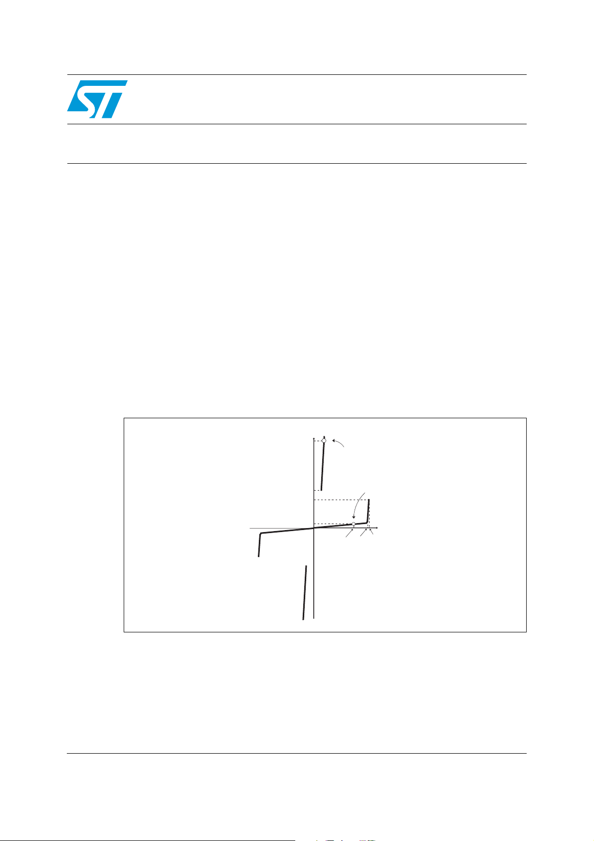
Figure 1. I / V characteristic of a Trisil
I
PP
I
H
I
BO
I
A
B
TM: Trisil is a trademark of STMicroelectronics
TM: Transil is a trademark of STMicroelectronics
RM
0
C
D
I
Transient
operation
Standby
operation
V
RMVBRVBO
V
July 2010 Doc ID 5649 Rev 3 1/13
www.st.com
Page 2
Trisil characteristics AN320
1 Trisil characteristics
1.1 Electrical characteristic
The electrical characteristic of the Trisil is similar to that of a Triac (see Figure 1) except that
the component has only two terminals.
Triggering in this case is not done via a gate but by an internal mechanism dependent on the
current flowing through it.
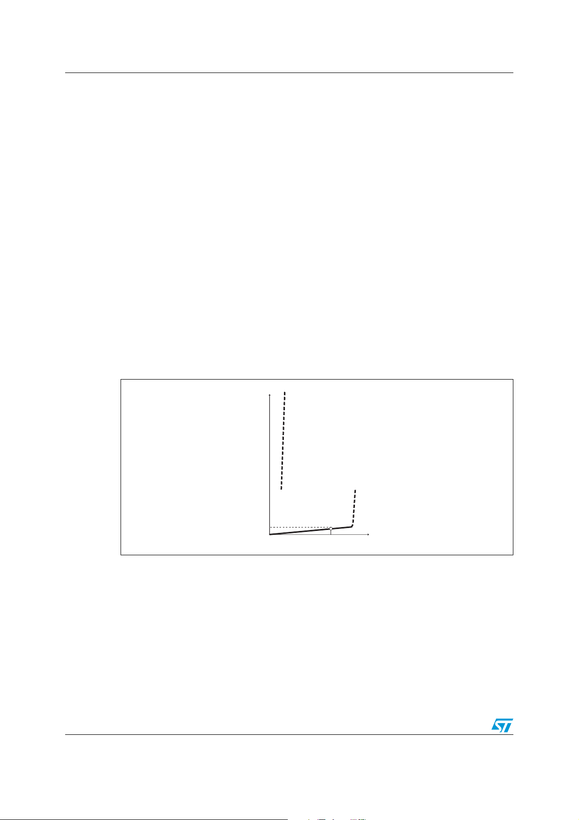
1.2 Operation seen from the outside
In normal operation, the Trisil is biased at a voltage lower than or equal to the standby
voltage (V
presence of the Trisil connected across the equipment to be protected does not disturb its
operation (see Figure 2).
The characteristic data at this point includes:
● Leakage current
● Electrical capacity
● Reliability of the component in blocking mode
). At that point of the characteristic, the leakage current is about 10 nA and the
RM
Figure 2. Stand by characteristics
I
I
RM
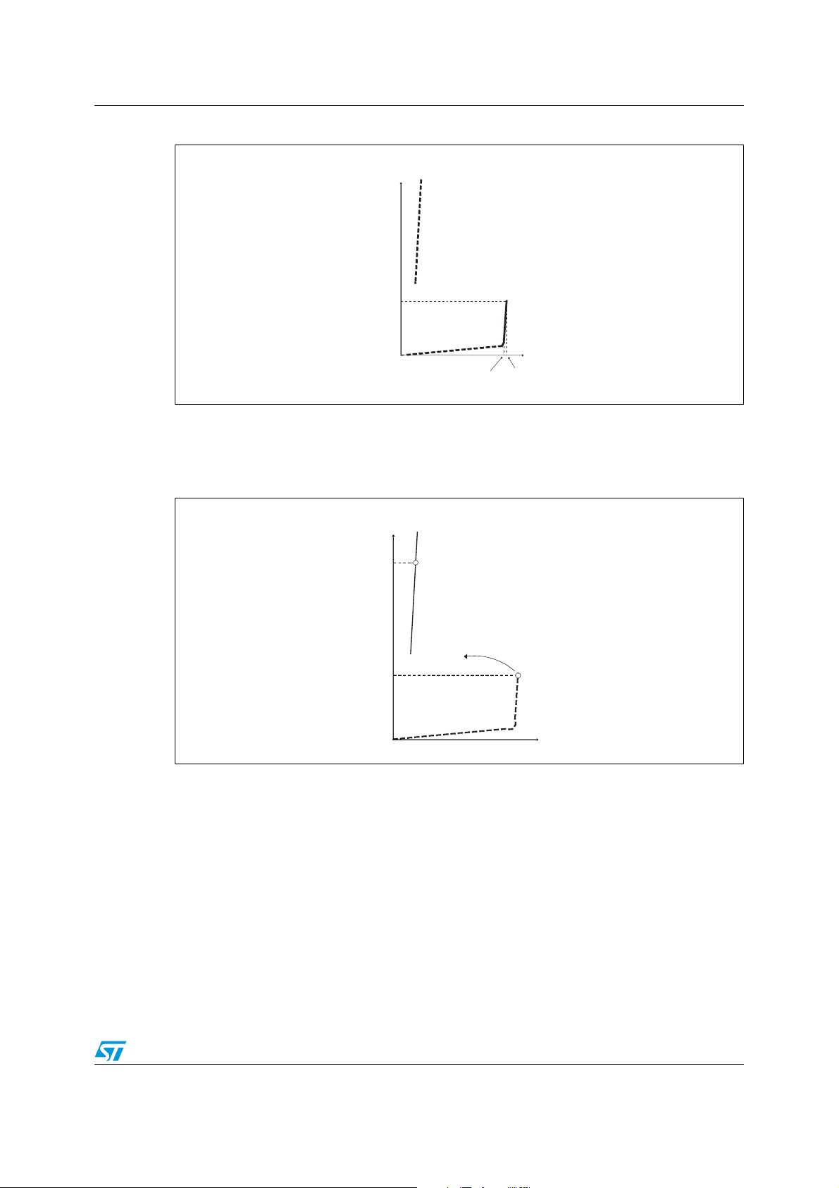
As the voltage increases beyond V
0
, the Trisil impedance drops from practically infinite to a
BR
V
RM
V
few ohms. The Trisil remains biased at its avalanche voltage and its operation is then
identical to that of a Transil diode (see Figure 3).
The characteristic parameters at this level are the limiting voltage (breakover voltage of the
component, V
) and the time for switching between the blocked and conducting states.
BO
2/13 Doc ID 5649 Rev 3
Page 3
AN320 Trisil characteristics
Figure 3. Avalanche characteristic of the Trisil
I
I
BO
V
VBRV
BO
For current values higher than I
, the voltage across the Trisil drops to a few volts and the
BO
high currents permitted without damage are possible due to the low value of this voltage,
since the physical limit is dependent on the dissipated power (see Figure 4).
Figure 4. Triggering, and on-state characteristics
I
I
PP
I
BO
V
The characteristic parameter is then the possibility of withstanding surge currents (peakpoint current, I
PP
).
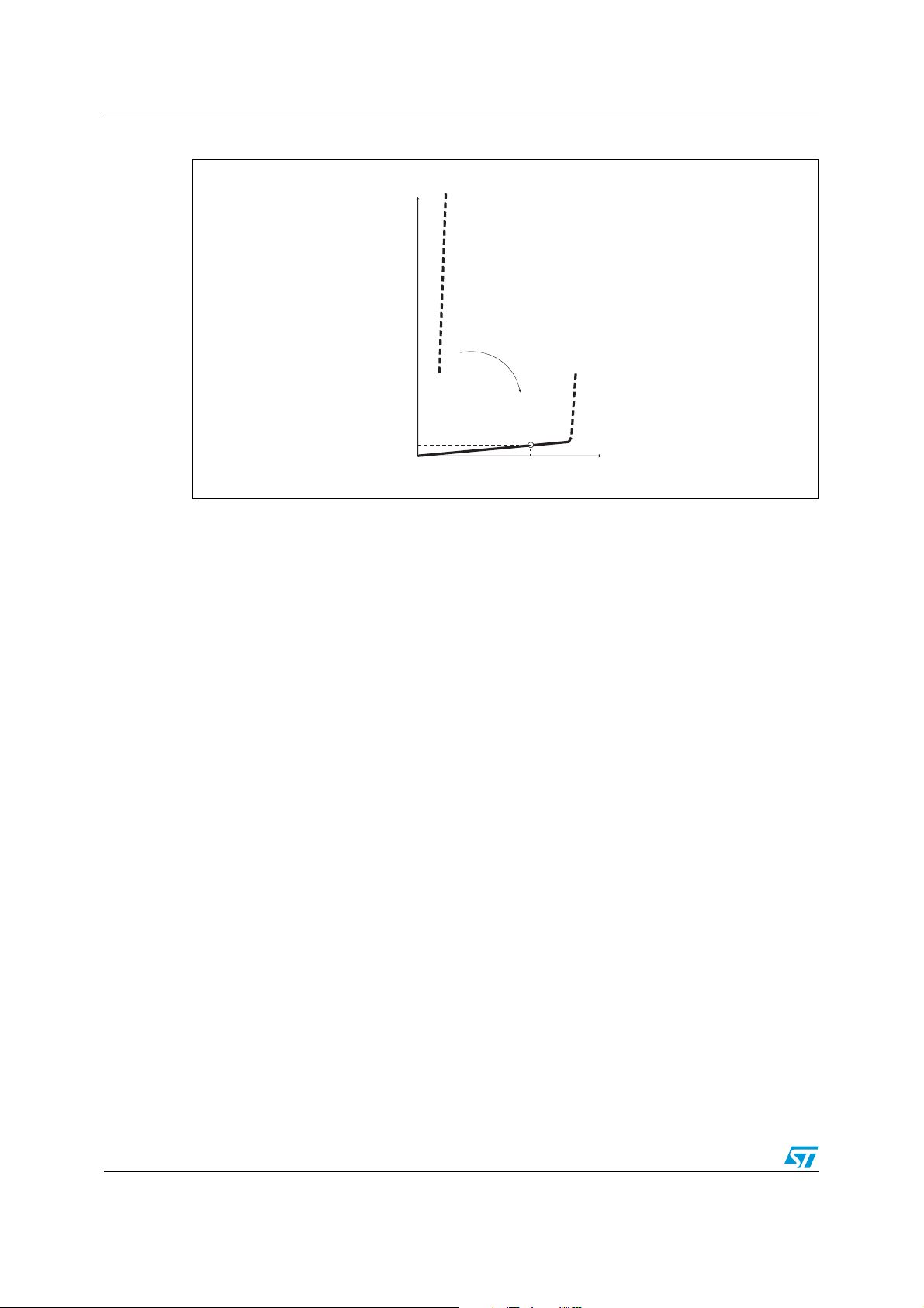
Return to standby operation by turning off the Trisil takes place when the current flowing
through it drops below I
. This is the characteristic parameter for switching from the
H
conducting to the blocked state (see Figure 5).
Doc ID 5649 Rev 3 3/13
Page 4
Trisil characteristics AN320
Figure 5. Return to standby operation
I
I
H
I
RM
0
V
RM
V
The surge current associated with the disturbance is diverted through the Trisil as soon as it
begins to operate in the avalanche mode (see Figure 3) and the voltage limitation results
from the electrical characteristic at this point. The behavior of the Trisil is here identical to
that of the Transil. The difference depends on the level of the breakover current, I
, where
BO
the triggering of the thyristor structures take place.
This phenomenon results in absolute limitation independently of the current level, and a
capacity to divert currents much higher than those possible for an avalanche diode (Transil).
Furthermore, this limitation is independent of the avalanche voltage of the device.
4/13 Doc ID 5649 Rev 3
Page 5

AN320 Trisil characteristics
A -T
il B -Trisil
1.3 Limiting property
Because of its operating mode, the Trisil results in absolute voltage limitation, independently
of the surge current level, Figure 6 and of the slope of the applied voltage ramp (see
Figure 7).
Figure 6. Correlation between the voltage and the surge current
rans
I
PP
I
PP
0
V
CL
0
V
BO
Figure 7. Correlation between the limiting voltage and the surge voltage ramp
V
V
BO
0
Voltage across
the Trisil
dV/dt
In particular, if the surge current is higher than the guaranteed value in the catalogue,
without however exceeding the physical limits of the component, the voltage across a Transil
could reach the critical value destroying the equipment to be protected. For a Trisil, this risk
is excluded.
Finally, for a surge current much higher than the guaranteed value, destruction of the Trisil
always results in a short-circuit thus providing absolute protection for the equipment located
downstream.
Doc ID 5649 Rev 3 5/13
Page 6
Trisil characteristics AN320
1.4 Behavior in case of current surges
The ability of semiconductor components to withstand high currents in transient operation is
limited for pulses longer than 10 ns by a second breakdown due to heat. This phenomenon,
although not destructive, is considered as the normal utilization limit in so far as the behavior
of the component depends on the external circuit.
The temperature rise within the semiconductor is thus the parameter which defines the
behavior of the component and its capacity to withstand current surges. It is given by
Equation 1:
Equation 1:
T
= TA + ZTH VON x I
j
With
● T
: instant temperature at the junction level
j
● T
● Z
● V
● I
: ambient temperature
A
: transient thermal impedance (as a function of the duration of the pulse)
TH
: voltage across the terminals of the component in the conducting state
ON
: transient current flowing through the component
RS
This equation clearly shows the advantage of the Trisil. A decrease in the voltage across its
terminals enables it to conduct a much higher current than the avalanche diode for the same
junction temperature. Since the voltage to be taken into consideration for the calculation is
that in the conducting state, the permitted current levels in transient operation are
independent of the avalanche voltage and the guaranteed values are identical for all the
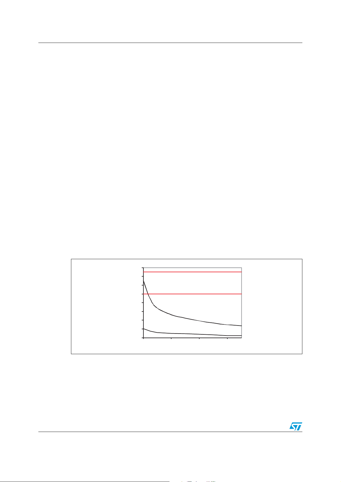
types of a given series (see Figure 8).
RS
Figure 8. Comparison of the limited transient currents for a Transil and a Trisil in
the similar cases (SMB).
I
(A)
PP
160
140
120
100
80
60
40
Transil
10/1000µs
20
0
50 100 150 200
Transil
8/20µs
VBR(V)
Trisil
8/20µs
Trisil
10/1000µs
The maximum junction temperature taken into account in transient operation is not that
given in the catalogues (junction temperature in operation or in storage) but corresponds,
with a certain safety margin, to the second breakdown due to thermal causes, i.e. about
350-400 °C.
This high current capacity can be applied in AC operation at the 50 Hz industrial frequency
(see Figure 9), which is particularly interesting in telephony where equipment should be
protected against overvoltages resulting from accidental coupling of the telephone line with
6/13 Doc ID 5649 Rev 3
Page 7

AN320 Trisil characteristics
the power distribution network. This type of protection is required by certain standards used
in telecommunications.
Figure 9. Long duration overload test
I(A)
10
–10
F = 50 Hz 10 pair of pulses
1.5 Response time
The response time of the component is the time it requires to limit the voltage. From this
point of view the Trisil has exactly the same behavior as a Transil. The time is that required
to switch from the standby operating point to the avalanche voltage. This is almost
instantaneous.
This time should not be confused with that required to pass from the breakover point (V
to the conducting characteristic. This time is longer but does not influence the limiting
capability of the device.
1.6 Operation within the avalanche area
This section concerns the segment VBR - VBO (see Figure 3) of the Trisil characteristic
between the blocked state and the conducting state at low V
This portion of the characteristic is identical to that of an avalanche diode. Thus within this
area, DC, AC or pulse-type operations are permitted. The currents are limited depending on
the possibilities of junction-ambient air heat dissipation. The maximum current is defined by
the following:
t(s)
112112 180
)
BO
.
ON
Equation 2:
T
= TA + RTH VBO I
j
MAX
≤ T
jMAX
= 150 °C
The condition when the Trisil is not triggered is defined as follows:
Equation 3:
I
< I
MAX
BO
The main differences from Equation 1 are:
● Maximum junction temperature which is now that given by the catalogue, i.e. 150 °C
● Voltage which is that of the avalanche mechanism
● Continuous thermal resistance replacing the transient thermal impedance
In AC operation, although Equation 2 still holds good, the voltage-current diagram as a
function of time shown in Figure 10 is clearer.
Doc ID 5649 Rev 3 7/13
Page 8

Trisil characteristics AN320
The value of the breakover current (IBO) plays an important part in the capacity of the device
in avalanche operation. If this value is high (see Figure 11A), the current in the component
must be limited by a suitable series resistor. For lower values, avalanche operation takes
place without destruction whatever the external circuit.
Figure 10. AC operation in the avalanche mode
R
S
I
V
S
V
T
V
BO
V
BR
T
V
T
V
S
Circuit
to be
protected
t
I
T
I
BO
t
–I
BO
Figure 11. Conditions for non destructive operation in the avalanche mode
A - Case in which the current should be limited by
the external circuit R
I
Destruction by
thermal effect P = Constant
VS/V
R
R
S
8/13 Doc ID 5649 Rev 3
> limit R
S
Limit R
S
S
I
BO
V
V
S
B - Correct operation whatever the external circuit
I
Destruction by
thermal effect P = Constant
I
BO
V
Page 9

AN320 Physical operation
2 Physical operation
A Trisil consists of two thyristors connected back to back. It will suffice to explain the
operation of one thyristor. The other operates in the same way if the voltage across the
component is reversed.
Figure 12. Operation in the blocked mode
()
N
N
I
N+ +
1
Leakage current
C
P1+
N
P
N+ +
1
2
+
2
B
A
J
1
J
2
J
3
V
Doc ID 5649 Rev 3 9/13
Page 10
Physical operation AN320
Figure 13. Operation in the avalanche mode
()
N
N
I
N+ +
1
Avalanche current
C
P1+
P
Application of a negative voltage on cathode N++ results in forward biasing of junctions J
and J
and reverse biasing of J2. The current observed is thus the leakage current of
3
junction J
. When the voltage exceeds a certain value, junction J2, which is reverse biased,
2
N+ +
1
+
2
B
A
J
1
J
2
J
3
V
1
begins to operate in the avalanche mode. The structure up to this current level operates like
a diode (junction J
The highly doped N
same potential as the N
). The side current biases the P1 layer next to the N1 part of the emitter.
2
layer has the same potential. The P1 area at the surface is forced to the
1
region by metallization.
1
10/13 Doc ID 5649 Rev 3
Page 11

AN320 Physical operation
Figure 14. Thyristor effect of the Trisil
()
N
N
I
+
C
N++
1
-
N
P
N++
1
P1+
2
+
2
B
A
J
1
J
2
J
3
V
As the avalanche current increases, this difference of potential can reach the threshold of
0.6 V, a value which is sufficient to create injection of electrons from the cathode towards the
P
area and thus trigger thyristor N1 P1 N2 P2.
1
The electrons thus injected into P
effect of the electrical field operating in the space charge of the reverse biased J
In N
, the electrons help to reduce the potential of this area compared with P2 and as a
2
result inject holes from P
towards N2. These holes travel in the reverse direction because of
2
their polarity. When they arrive at P
N
, this time resulting in the injection of electrons from N1 to P1.
1
The procedure is cumulative. The excess electrons in N
compensate the fixed charges of the space charge and will thus suppress it. Junction J
in fact will reach J2 by diffusion, and cross it under the
1
they help to increase the potential of P1 with respect to
2
and the holes in P1 will
2
junction.
2
will
2
act as a forward biased junction and the voltage across the component will drop.
Doc ID 5649 Rev 3 11/13
Page 12

Revision history AN320
3 Revision history
Table 1. Document revision history
Date Revision Changes
February-1998 1 First issue.
10-May-2004 2 Stylesheet update. No content change.
05-Jul-2010 3 Updated trademark statements.
12/13 Doc ID 5649 Rev 3
Page 13

AN320
Please Read Carefully:
Information in this document is provided solely in connection with ST products. STMicroelectronics NV and its subsidiaries (“ST”) reserve the
right to make changes, corrections, modifications or improvements, to this document, and the products and services described herein at any
time, without notice.
All ST products are sold pursuant to ST’s terms and conditions of sale.
Purchasers are solely responsible for the choice, selection and use of the ST products and services described herein, and ST assumes no
liability whatsoever relating to the choice, selection or use of the ST products and services described herein.
No license, express or implied, by estoppel or otherwise, to any intellectual property rights is granted under this document. If any part of this
document refers to any third party products or services it shall not be deemed a license grant by ST for the use of such third party products
or services, or any intellectual property contained therein or considered as a warranty covering the use in any manner whatsoever of such
third party products or services or any intellectual property contained therein.
UNLESS OTHERWISE SET FORTH IN ST’S TERMS AND CONDITIONS OF SALE ST DISCLAIMS ANY EXPRESS OR IMPLIED
WARRANTY WITH RESPECT TO THE USE AND/OR SALE OF ST PRODUCTS INCLUDING WITHOUT LIMITATION IMPLIED
WARRANTIES OF MERCHANTABILITY, FITNESS FOR A PARTICULAR PURPOSE (AND THEIR EQUIVALENTS UNDER THE LAWS
OF ANY JURISDICTION), OR INFRINGEMENT OF ANY PATENT, COPYRIGHT OR OTHER INTELLECTUAL PROPERTY RIGHT.
UNLESS EXPRESSLY APPROVED IN WRITING BY AN AUTHORIZED ST REPRESENTATIVE, ST PRODUCTS ARE NOT
RECOMMENDED, AUTHORIZED OR WARRANTED FOR USE IN MILITARY, AIR CRAFT, SPACE, LIFE SAVING, OR LIFE SUSTAINING
APPLICATIONS, NOR IN PRODUCTS OR SYSTEMS WHERE FAILURE OR MALFUNCTION MAY RESULT IN PERSONAL INJURY,
DEATH, OR SEVERE PROPERTY OR ENVIRONMENTAL DAMAGE. ST PRODUCTS WHICH ARE NOT SPECIFIED AS "AUTOMOTIVE
GRADE" MAY ONLY BE USED IN AUTOMOTIVE APPLICATIONS AT USER’S OWN RISK.
Resale of ST products with provisions different from the statements and/or technical features set forth in this document shall immediately void
any warranty granted by ST for the ST product or service described herein and shall not create or extend in any manner whatsoever, any
liability of ST.
ST and the ST logo are trademarks or registered trademarks of ST in various countries.
Information in this document supersedes and replaces all information previously supplied.
The ST logo is a registered trademark of STMicroelectronics. All other names are the property of their respective owners.
© 2010 STMicroelectronics - All rights reserved
STMicroelectronics group of companies
Australia - Belgium - Brazil - Canada - China - Czech Republic - Finland - France - Germany - Hong Kong - India - Israel - Italy - Japan -
Malaysia - Malta - Morocco - Philippines - Singapore - Spain - Sweden - Switzerland - United Kingdom - United States of America
www.st.com
Doc ID 5649 Rev 3 13/13
 Loading...