


AN3169
Application note
Technology performance comparison of Triacs
subjected to fast transient voltages
Introduction
This paper presents an experimental comparison of several Triac devices under immunity
tests, as described in the IEC 61000-4-4 standard. After a short reminder of the different
Triac technologies available today (Top, mesa and planar technologies), the IEC 61000-4-4
test procedure to compare the devices is explained. The immunity results are discussed
according to the device technology and the gate current sensitivities. A discussion about
relevance of dV/dt parameter and die area is carried on to differentiate the devices in term of
immunity capability.
Home appliances such as washing machines, refrigerators and dishwashers integrate a lot
of low power loads such as valves, door lock systems, dispensers and drain pumps. These
loads are usually powered by the mains in on / off mode, and are mostly controlled by Triacs.
The direct connection of the silicon switch to the mains, through the load, requires that these
devices must withstand line transients to make the system compliant with the international
electromagnetic compatibility (EMC) standards. The silicon devices are then subjected to
fast transient voltages, as described in the IEC/EN 61000-4-4 standard.
The immunity of several Triac technologies is evaluated here experimentally. Several
guidelines can then be pointed out to design high immunity appliances.
March 2010 Doc ID 17194 Rev 1 1/12
www.st.com
Triac technologies and immunity AN3169
1 Triac technologies and immunity
1.1 Triac silicon structures
Triac devices are by far the most used silicon devices to drive AC loads directly connected
on the mains voltage. Triacs are widely used because they present three major advantages:
● Low forward voltage drop
● Turn on by gate current pulse
● High voltage immunity
The first two advantages come from the active silicon structure of the Triac which is based
on four alternatively doped silicon layers (N-P-N-P). These four layers implement two bipolar
transistors which are coupled to maintain the on state even if the gate current is removed
(see Figure 1).
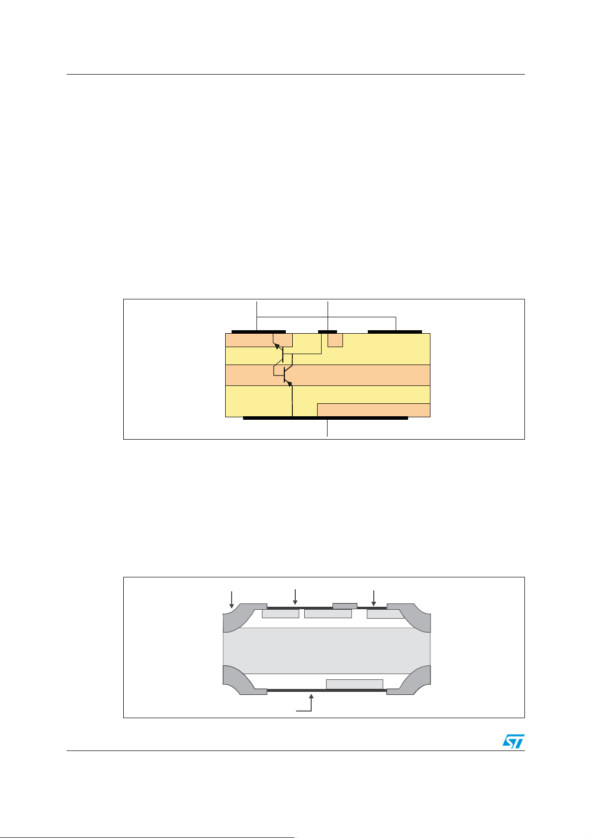
Figure 1. Active simplified structure of a Triac
A1 G
N4
N1
N1
P1
P1
N4
P1
P1
N2
N2
P2
P2
A2
N2
N2
P2
P2
N3
N3
The third advantage comes from the fact that the voltage is withstood by the silicon
thickness. It's then quite easy to reach breakdown levels above 1 kV. The main issue is then
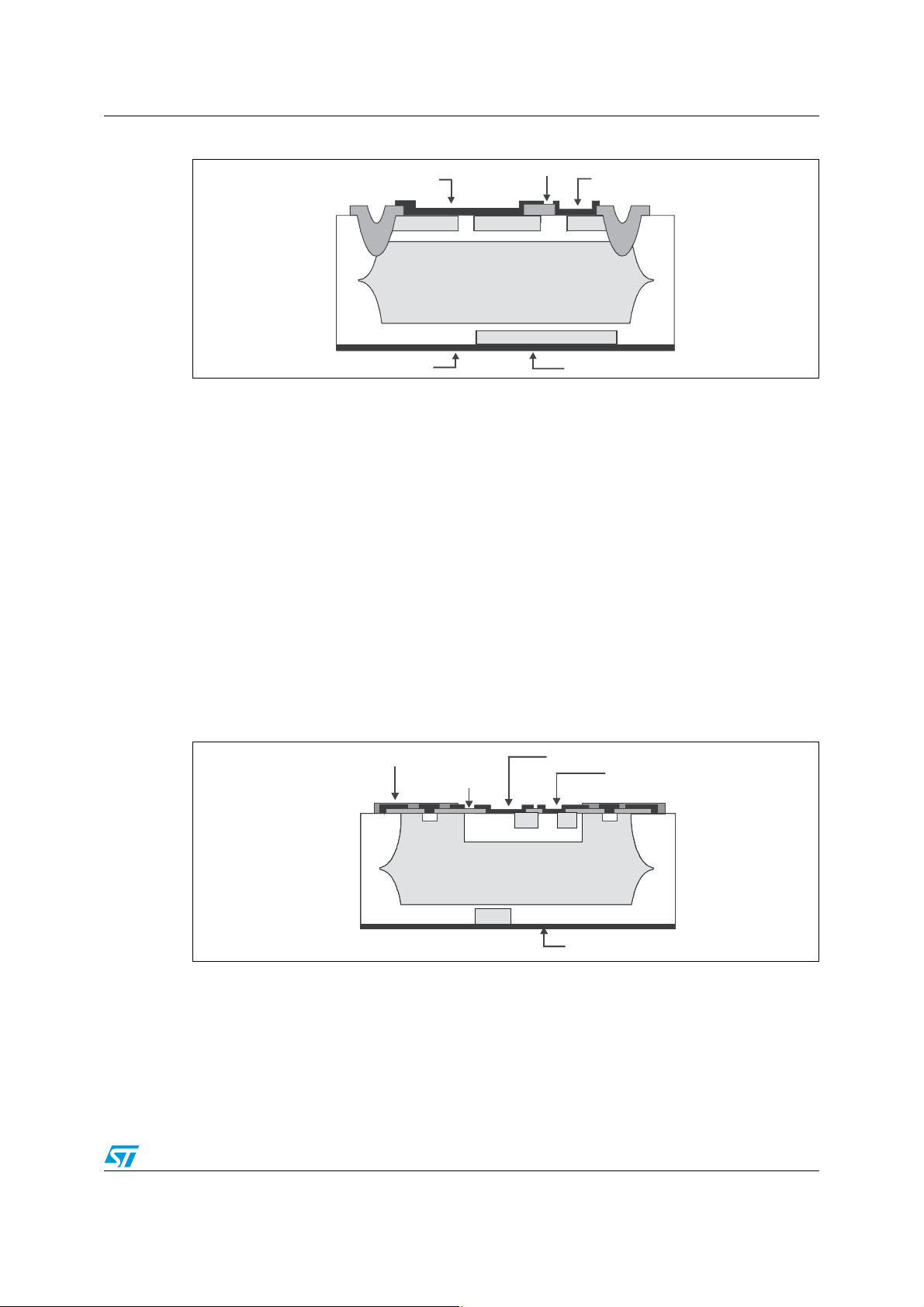
the junction termination. Several low cost technologies are used since the 70’s which used a
glass passivation. For example the “Mesa” technology (see Figure 2) uses glass on both
sides of the die (see References 1, 2, and 3) to passivate both junctions, which hold both
forward and reverse high voltages (referred to as “Cathode” or “A1” or “COM” polarity). The
“Top” glass technology (see References 1, 2, and 3) uses only one glass layer (see
Figure 3). This avoids having some glass at the bottom of the die, and so it is easier to put
such dies in every kind of package.
Figure 2. “Mesa” glass technology
Glass
Cathode
N
N
P
Gate
NN
P
Metalization
2/12 Doc ID 17194 Rev 1
N
Anode
AN3169 Triac technologies and immunity
Figure 3. “Top” glass technology
Cathode
Glass
Gate
NN
P
Anode
N
P
N
+
Metalization
N
P
Both top and mesa glass technologies are very cost effective. The insulation capability of
glass is very high. This helps to achieve high voltage devices with a limited periphery area.
Mesa glass technology is the cheaper one as this technology uses less silicon area to
withstand reverse voltage. For top technology, the reverse PN junction is terminated on the
upper side of the die thanks to the deep P well. Such dies are bigger for the same active
area than mesa dies. This is the reason why top technology is mainly used for low current
Triacs.
Unfortunately it is not possible to ensure a good operation of a die with glass passivation
when the voltage exceeds its maximum allowed value (V
DRM
or V
parameters). If the
RRM
voltage reaches the breakdown value, a current will flow through the die periphery, causing
heat dissipation at the glass-silicon interface. This heat could cause mechanical stress and
damage this interface. The device could then be damaged.
To develop switches able to work up to their breakdown voltage, a planar technology has to
be implemented. Such a technology uses photolithography to terminate the PN junction at
the top of the die, and oxide passivation instead of glass (see Figure 4). There is no more
glass-silicon interface issue. ACST devices use this kind of technology (see Reference 4).
Figure 4. Planar technology
Passivation
P
P
Doc ID 17194 Rev 1 3/12
Oxyde
Anode
N
NN
N N
N N
N
N
Cathode
P
P
Metalization
Gate
P
P

Triac technologies and immunity AN3169
1.2 Sensitivity and dV/dt immunity
This experimental comparison on immunity level has been performed on different devices
which target the same application. This application is the control of valves or pumps in white
goods. The load current is usually less than 1 A. Anyway, appliances designers use, to
control these loads, 1 A, 2 A and even 4 A Triacs. The use of a high current rating device is
usually motivated by desire for highly immune and robust systems.
To rationally compare the different devices, we have selected devices with the same voltage
and sensitivity ratings. The voltage rating is given by the V
in this application note). The sensitivity is given for Triacs by the I
minimum gate current that should be applied to turn on the device. The devices we have
chosen all have a 10 mA maximum I
GT
.
The Triac sensitivity can not be reduced too much. An appliance designer has to work with
the sensitivity (supply consumption) and immunity compromise. If the I
device will not be able to withstand excessive dV/dt rates across its power terminals (A1 and
A2 for Triacs, or OUT and COM for ACST). Triac manufacturers then give a dV/dt parameter
which is measured at the maximum junction temperature. Results of Ta b le 1 are given for
dV/dt tests performed at a 125 °C junction temperature and a 400 V applied voltage. It
should be noted that some values are lower than values given in constructors datasheet for
the devices which are specified at 110 °C instead of 125 °C. This is a normal result as the
dV/dt immunity decreases with the temperature.
DRM
and V
GT
parameters (800 V
RRM
parameter which is the
is too low, the
GT
Ta bl e 1 gives the I
and dV/dt parameters that we measured for the different samples we
GT
used during IEC 61000-4-4 tests, and for the different bias polarities.
The products tested are:
● the Z0409N: a top glass 4 A Triac
● the T410-800: a mesa glass 4 A Triac
● the ACST2: a planar 2 A Triac
● the COMP.1A: a planar 1 A Triac
● the COMP.2A: a planar 2 A Triac
4/12 Doc ID 17194 Rev 1

AN3169 Triac technologies and immunity
Table 1. Measured IGT and dV/dt parameters of tested samples
I
(mA) dV/dt (V/µs) 125 °C
gt
P/N Techno. Sample
Q1 Q2 Q3 Positive Negative
1 1.02 3.37 4.69 118 94
2 0.90 2.90 3.49 140 135
Z0409N Top
3 1.02 2.99 4.08 120 95
4 0.98 2.72 3.69 160 138
1 1.57 5.82 3.43 200 450
2 1.67 7.14 3.69 180 710
T410-800 Mesa
3 1.52 5.43 3.31 180 525
4 1.65 6.99 3.64 170 630
1 3.54 6.20 6.83 >5000 >5000
2 3.48 6.20 6.82 >5000 >5000
ACST2 Planar
3 3.45 6.20 6.83 >5000 >5000
4 3.47 6.20 6.73 >5000 >5000
1 4.89 4.05 5.10 500 470
2 4.85 4.28 5.22 580 500
COMP.1A Planar
3 4.86 4.05 5.05 530 430
4 4.85 4.16 5.34 540 560
1 5.27 6.25 5.65 >5000 >5000
(1)
COMP.2A Planar
2 4.57 4.36 4.27 >5000 >5000
3 3.81 3.39 3.09 >5000 >5000
4 4.82 4.68 4.49 >5000 >5000
is measured with standard 30 Ω / 12 V circuit and dV/dt with standard test circuit: open gate and
1. I
GT
400 V applied peak voltage
Doc ID 17194 Rev 1 5/12

IEC 61000-4-4 Tests AN3169
2 IEC 61000-4-4 Tests
2.1 Test procedure
To compare the immunity capabilities of the different technologies, we have performed tests
as described in the IEC 61000-4-4 standard [5]. European appliance manufacturers usually
require that their equipment will not present any malfunction for burst levels up to 2 kV.
Here, we increase the burst level by 0.1 kV steps to reach at least one device spurious
triggering within one minute. To easily compare only the Triacs performance, we used a
dedicated board featuring all the AC switches, and their gate connected to their A1 terminals
through gate resistors. This allows us to be sure that the spurious triggering comes from the
switch itself and not from any control circuit. The spurious triggering is detected when the
light bulb, connected in series with one of the switch, is switched on. As a Triac will latch,
usually the on time will last several ms. This is long enough for a human eye to detect it.
The tests are carried out in the following conditions.
● The printed circuit board is 10 cm above reference plane.
● A mains S14K300 varistor (refer to “V” on Figure 5) is connected to the mains input on
the PCB.
● The board embeds four Triacs (or ACSTs).
● Each Triac-A2 (or ACST OUT) terminal is linked to a 25 W light bulb (resistive loads are
chosen to get easier device turn on as dI/dt is higher than with inductive load).
● Each gate is connected to A1 or COM terminals respectively, for Triac and ACST,
through a 220 ohm resistor (refer to “R
coming from any control circuit.
● No snubber circuits are added across the Triacs or ACSTs.
● Ambient temperature is 25° C.
● The board is plugged into an L-N plug which is disturbed by a burst generator (bursts
are coupled to N or to L, for positive or negative bias).
● The burst generator is programmed as required in the IEC 61000-4-4 standard (15 ms
burst duration, 3 Hz burst frequency, 5 kHz spike frequency, one minute test duration).
” on Figure 5) to be free of spurious firings
g
Note: Only results with coupling modes to L and N are presented here as the other coupling
modes are usually less stressful. For example, a simultaneous coupling of the burst to L, N
and the PE (Protective Earth, which is not connected to our board) will lead to a less
stressful test.
6/12 Doc ID 17194 Rev 1

AN3169 IEC 61000-4-4 Tests
Figure 5. IEC 61000-4-4 test schematic
L
V
V
Rg
N
2.2 Impact of a varistor on mains input
The IEC 61000-4-4 standard as been developed mainly to protect equipment from fast
voltage transients coming from bad mains connection, electrostatic discharge or inductive
load disconnection. Designers usually think that the impact of the burst is mainly due to the
high dV/dt, and so due to the capacitive currents circulating through all parasitic capacitors.
This effect is one of the major ones. Applying bursts can also cause some spurious device
turn on due to excessive voltage across the switches. For example, Figure 6 shows the
voltage and current waveforms of an ACST2 used in the previously described board but
without any varistor for a 1 kV burst. We see that when the voltage spikes are applied at
peak mains voltage, the device turns on, and turns off for the next ZCS (zero current
switching) point. If we zoom in on this oscillogram with a 0.4 µs/division time scale, we
clearly see that the triggering comes from an overvoltage. Indeed, Figure 7 shows that the
voltage across the ACST2 reaches more than 800 V, and then the device turns on in
breakover mode.
Such a turn on can be allowed with ACST2 devices, contrary to other technologies and even
contrary to other planar devices from other companies. For ACST2 there will not be any risk
of device failure, as long as the applied current remains below the guaranteed limit. But,
applying such bursts without any voltage protection on mains input could lead to devices
failure with top or mesa glass technologies. This is the reason why we put a varistor on the
board we used for IEC 61000-4-4 tests.
Figure 6. ACST2 behavior during 1 kV burst (without input varistor)
V
V
OUT-COM
OUT-COM
I
I
OUT
OUT
Doc ID 17194 Rev 1 7/12

IEC 61000-4-4 Tests AN3169
Figure 7. ACST2 turn on zoom (without input varistor)
V
V
OUT-COM
OUT-COM
I
I
OUT
OUT
2.3 Technology impact on immunity levels
Immunity test results according to P/N are given in Figure 8. This graphic gives the
maximum burst levels that the different devices were able to withstand before turn on. We
see that most of the devices present highly dispersed results. Even if these tests have been
performed with devices with a low dispersion on I
Ta bl e 1 ), their immunity levels can vary with a 1 to almost 3 scale. The coupling mode and
burst polarity also have an impact on the immunity capability of a sample. This impact can
vary between 20 to 60%. Only the minimum value of the “maximum burst level” range, given
in Figure 8, should be taken into account. This minimum level corresponds to the worst-case
operation among all the different coupling cases covered by the IEC 61000-4-4 standard.
levels (for the same product, refer to
GT
It should be also noted that the maximum capability of our burst generator is 4.5 kV. That
means that we didn't succeed in reaching the maximum immunity level of most ACST2
devices.
These results offer several interesting considerations.
● The planar technology allows the highest level to be reached, but different companies
do not reach the same level.
● ACST2 supports levels twice as high as its closest competitor (COMP.2A).
● The 2 A device (COMP.2A) in planar technology is approximately as immune as the 4 A
Triac in mesa glass technology.
● A device which presents a good dV/dt immunity (around 500 V/us for COMP.1A) can
only be as immune as a 4 A top device with a dV/dt capability close to 100 V/us.
Concerning the last point, it should be noted that the COMP.1A device presents a die area
which is approximately 20% lower than the Z0409. And generally speaking it can be said
that the bigger the die area is, the higher the immunity level is. Only the ACST2, which
presents the highest immunity level, presents also the highest “immunity-level-to-die-area”
ratio.
Indeed, its die area is almost half that of the T410-800 for twice the immunity.
Compared to COMP.2A, this “immunity-area” ratio is also 40% higher. To reach
approximately the same immunity level (2.4 KV in average, compare to 3 kV with ACST2), a
47 nF - 100 ohm snubber circuit has to be added across the COMP.2A device.
8/12 Doc ID 17194 Rev 1

AN3169 IEC 61000-4-4 Tests
Figure 8. Product rankings in IEC 61000-4-4 tests
ACST2
T410-800
Z0409N
COMP.1A
COMP.2A
0 0.5 1 1.5 2 2.5 3 3.5 4 4.5
Max burst levels (kV)
2.4 Sensitivity impact
According to previous results, it is difficult to conclude anything about impact of device
sensitivity on immunity. We have even seen that some devices with good dV/dt capability
can present poor immunity level. But, such a conclusion is difficult to sustain because we
have compared here components from different processes.
To better analyze the sensitivity impact, we have also performed some tests of other Triacs
coming from the same process. We took some T405-800 devices which are manufactured
with the same process as the T410-800. The T405-800 device is guaranteed to present I
currents of less than 5 mA. The samples we have tested present measured I
levels
GT
approximately half those of the T410 devices we have tested, and this for the three
quadrants. It means that we measured an I
level of approximately 0.75 mA, 2.30 mA and
GT
1.75 mA respectively for quadrants 1, 2 and 3. The maximum burst level that these devices
were able to withstand was around 1 kV, i.e. 30% lower than the T410-800. This result
highlights that sensitivity has also a strong impact on immunity, as is well known. But this
statement is only valid if one compares two devices from the same process.
GT
Doc ID 17194 Rev 1 9/12

Conclusion AN3169
3 Conclusion
This application note has given experimental benchmarking analysis among different
alternating current switch offerings. The impacts of silicon process technologies and
sensitivity levels have been discussed. It has thus been shown that sensitivity and dV/dt
parameters are not relevant enough to evaluate the immunity rating of different devices. A
lower I
silicon process. It has been furthermore shown that the die area has also a big impact on
immunity. Indeed, a bigger die area will lead to a higher device capacitance. This will help to
absorb energy coming from the bursts, and thus reducing the dV/dt across the device. On
the other hand, when dV/dt immunity of Triacs is measured, the voltage rate is forced across
the device. So a bigger die area will lead to a higher capacitive current. So a bigger device,
with the same sensitivity level, will withstand a lower dV/dt level.
Planar technology seems to offer devices with the highest immunity. However, Z04 and T410
devices, respectively produced with a top and mesa technologies, offer the same minimum
level of immunity as the tested planar devices. ACST2 presents the highest immunity level
compared to other technologies or compared to other planar devices from other companies.
ACST2 can then be used without any snubber circuit with a high immunity to bursts and is
the solution for applications requiring a high immunity level.
will lead to a less immune device but only if we compare devices from similar
GT
4 References
1. J. Arnould, P. Merle, “Dispositifs de l'Electronique de Puissance”, Vol. 2, HERMES
edition, 1992, ISBN 2-86601-308-5.
2. STMicroelectronics, “SCRs, Triacs and AC Switches Quality and Reliability”, SCRs,
Triacs and AC Switches databook, 4th Edition, 2001.
3. B. Morillon, “Study of Aluminum Thermomigration in Silicon for the Industrial
Implementation of Isolation Walls in Bidirectioanl Power Devices”, Ph.D. Dissertation,
Institut National des Sciences Appliquées de Toulouse, Toulouse (France), July 2002.
4. STMicroelectronics, “ACST2 series - AC Switch family”, datasheet, Rev.1, March 2007.
5. L. Gonthier, “ACS and Triacs Comparison towards Fast Voltage Transients”, conf.
Power Conversion Intelligent Motion, PCIM 2000, Nuremberg, Germany, 2000, Proc.
CD-ROM.
10/12 Doc ID 17194 Rev 1

AN3169 Revision history
5 Revision history
Table 2. Document revision history
Date Revision Changes
09-Mar-2010 1 Initial release.
Doc ID 17194 Rev 1 11/12

AN3169
Please Read Carefully:
Information in this document is provided solely in connection with ST products. STMicroelectronics NV and its subsidiaries (“ST”) reserve the
right to make changes, corrections, modifications or improvements, to this document, and the products and services described herein at any
time, without notice.
All ST products are sold pursuant to ST’s terms and conditions of sale.
Purchasers are solely responsible for the choice, selection and use of the ST products and services described herein, and ST assumes no
liability whatsoever relating to the choice, selection or use of the ST products and services described herein.
No license, express or implied, by estoppel or otherwise, to any intellectual property rights is granted under this document. If any part of this
document refers to any third party products or services it shall not be deemed a license grant by ST for the use of such third party products
or services, or any intellectual property contained therein or considered as a warranty covering the use in any manner whatsoever of such
third party products or services or any intellectual property contained therein.
UNLESS OTHERWISE SET FORTH IN ST’S TERMS AND CONDITIONS OF SALE ST DISCLAIMS ANY EXPRESS OR IMPLIED
WARRANTY WITH RESPECT TO THE USE AND/OR SALE OF ST PRODUCTS INCLUDING WITHOUT LIMITATION IMPLIED
WARRANTIES OF MERCHANTABILITY, FITNESS FOR A PARTICULAR PURPOSE (AND THEIR EQUIVALENTS UNDER THE LAWS
OF ANY JURISDICTION), OR INFRINGEMENT OF ANY PATENT, COPYRIGHT OR OTHER INTELLECTUAL PROPERTY RIGHT.
UNLESS EXPRESSLY APPROVED IN WRITING BY AN AUTHORIZED ST REPRESENTATIVE, ST PRODUCTS ARE NOT
RECOMMENDED, AUTHORIZED OR WARRANTED FOR USE IN MILITARY, AIR CRAFT, SPACE, LIFE SAVING, OR LIFE SUSTAINING
APPLICATIONS, NOR IN PRODUCTS OR SYSTEMS WHERE FAILURE OR MALFUNCTION MAY RESULT IN PERSONAL INJURY,
DEATH, OR SEVERE PROPERTY OR ENVIRONMENTAL DAMAGE. ST PRODUCTS WHICH ARE NOT SPECIFIED AS "AUTOMOTIVE
GRADE" MAY ONLY BE USED IN AUTOMOTIVE APPLICATIONS AT USER’S OWN RISK.
Resale of ST products with provisions different from the statements and/or technical features set forth in this document shall immediately void
any warranty granted by ST for the ST product or service described herein and shall not create or extend in any manner whatsoever, any
liability of ST.
ST and the ST logo are trademarks or registered trademarks of ST in various countries.
Information in this document supersedes and replaces all information previously supplied.
The ST logo is a registered trademark of STMicroelectronics. All other names are the property of their respective owners.
© 2010 STMicroelectronics - All rights reserved
STMicroelectronics group of companies
Australia - Belgium - Brazil - Canada - China - Czech Republic - Finland - France - Germany - Hong Kong - India - Israel - Italy - Japan -
Malaysia - Malta - Morocco - Philippines - Singapore - Spain - Sweden - Switzerland - United Kingdom - United States of America
www.st.com
12/12 Doc ID 17194 Rev 1
 Loading...