

Page 1

AN3168
Application note
Non-insulated SCR / Triac control circuits
Introduction
In alternating current applications the direct current power supply for low-voltage electronic
devices (MCU, LEDs, optocouplers, Triacs and so on) can be provided using one of several
different circuits. There are traditionally two major types of power supplies used in
appliances, capacitive power supply and linear power supply using a step-down transformer.
Today, designers are using more and more switches mode power supplies (SMPS) to
achieve higher output current levels and especially lower standby power consumption. The
power supply choice is a trade-off between several parameters. These are the cost, the
required power, the output voltage level and polarity, the standby power consumption and
the necessity or not of an electrical insulation between the mains and the low output DC
voltage.
This application note considers only non-insulated power supplies. After a brief description
of the triggering quadrants and key parameters for SCR, Triac, ACS and ACST, the usual
control circuits are described according to the output voltage polarity of the power supply.
Finally, some examples of negative power supply circuits are introduced.
March 2010 Doc ID 17193 Rev 1 1/20
www.st.com
Page 2

AN3168 Contents
Contents
1 Triggering quadrants and key parameters . . . . . . . . . . . . . . . . . . . . . . . 3
2 Triggering circuits . . . . . . . . . . . . . . . . . . . . . . . . . . . . . . . . . . . . . . . . . . . 6
2.1 Two kind of power supply bias . . . . . . . . . . . . . . . . . . . . . . . . . . . . . . . . . . 6
2.2 Gate resistor value definition . . . . . . . . . . . . . . . . . . . . . . . . . . . . . . . . . . . 6
2.3 SCR and Triac triggering circuit with a positive power supply . . . . . . . . . . 7
2.4 Triac and ACS / ACST triggering circuit with negative power supply . . . . . 8
2.5 SCR triggering circuit with negative power supply . . . . . . . . . . . . . . . . . . . 9
2.6 Diac control circuit . . . . . . . . . . . . . . . . . . . . . . . . . . . . . . . . . . . . . . . . . . 10
3 Examples of negative power supplies . . . . . . . . . . . . . . . . . . . . . . . . . 12
3.1 Linear power supply . . . . . . . . . . . . . . . . . . . . . . . . . . . . . . . . . . . . . . . . . 12
3.2 Capacitive power supply . . . . . . . . . . . . . . . . . . . . . . . . . . . . . . . . . . . . . 13
3.3 Resistive power supply . . . . . . . . . . . . . . . . . . . . . . . . . . . . . . . . . . . . . . . 14
3.4 Buck-boost power supply . . . . . . . . . . . . . . . . . . . . . . . . . . . . . . . . . . . . . 15
3.5 Flyback power supply . . . . . . . . . . . . . . . . . . . . . . . . . . . . . . . . . . . . . . . . 17
3.6 Comparison of negative power supplies . . . . . . . . . . . . . . . . . . . . . . . . . 18
4 Conclusion . . . . . . . . . . . . . . . . . . . . . . . . . . . . . . . . . . . . . . . . . . . . . . . . 19
5 References . . . . . . . . . . . . . . . . . . . . . . . . . . . . . . . . . . . . . . . . . . . . . . . . 19
6 Revision history . . . . . . . . . . . . . . . . . . . . . . . . . . . . . . . . . . . . . . . . . . . 19
Doc ID 17193 Rev 1 2/20
Page 3
AN3168 Triggering quadrants and key parameters
1 Triggering quadrants and key parameters
To switch-on an SCR, Triac, ACS or ACST, a gate current must be applied on its gate pin
(G). The gate current flows between Gate (G) and Cathode (K) for SCR, or between Gate
and terminal A1 for Triac, or between Gate and terminal COM for ACS and ACST.
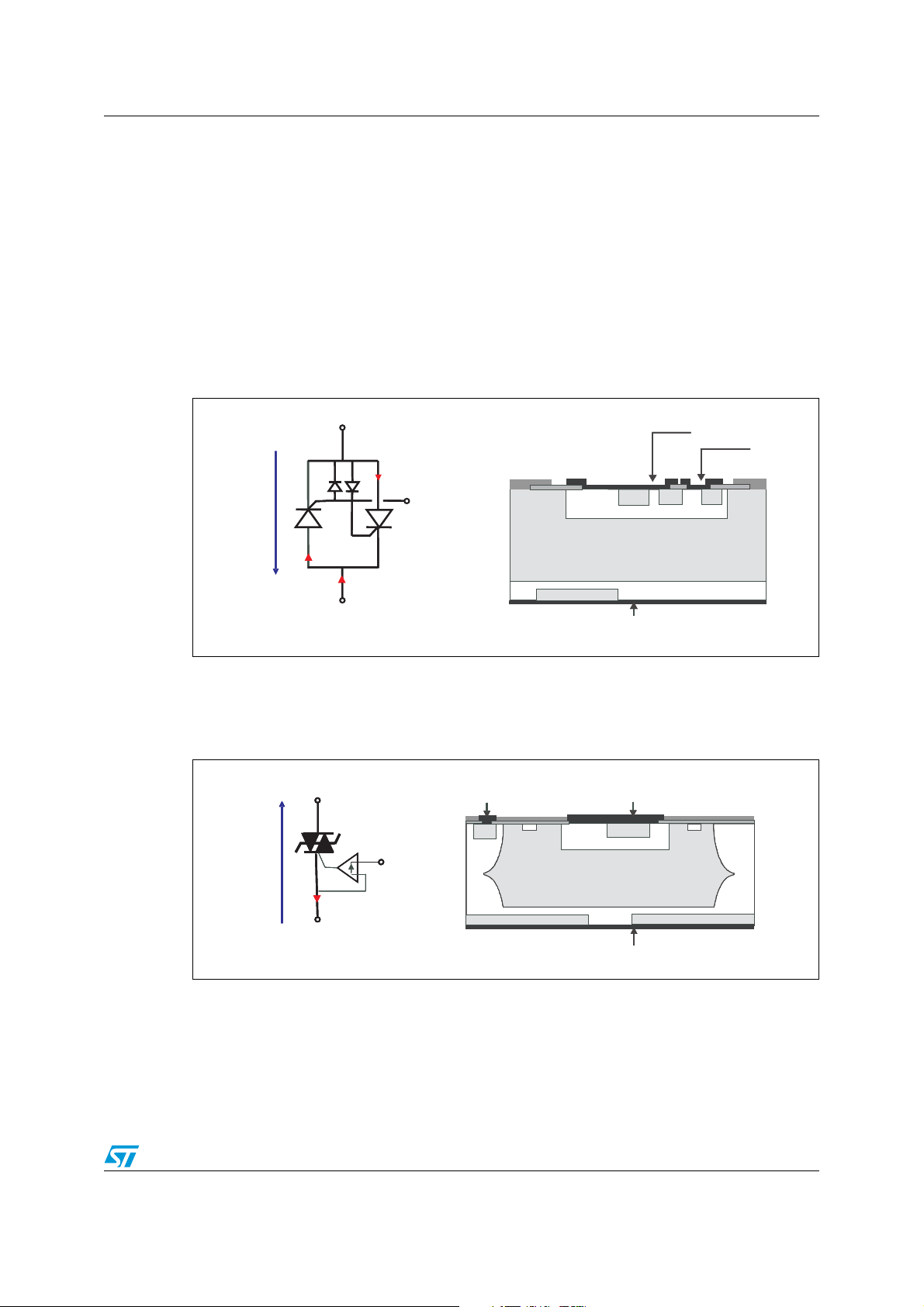
For Triac and ACST, the gate current could be positive or negative. Figure 1 illustrates the
simplified schematic of a Triac or an ACST and the associated silicon structure. A Triac or an
ACST could be switched on by a positive or a negative gate current through the diodes
embedded back-to-back between G and A1. These 2 diodes are implemented at the P1-N1
and P1-N2 junctions.
Figure 1. Simplified schematic and silicon structure of Triac / ACST circuit
N2 N1
N2 N1
P1
P1
N
N
A1 (or COM)
G
A1 (or COM)
I
I
-
-
V
T
I
+
I
T
G
A2 (or OUT)
N+
N+
N2
N2
P
P
A2 (or OUT)
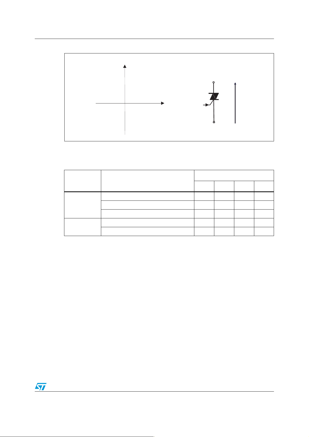
The silicon structure of an ACS is different from a Triac or an ACST (see Figure 2). Here the
gate is the emitter of a NPN bipolar transistor. So there is only one PN junction implemented
by P1 and N1. The gate current can then only be sunk from the gate, and not sourced to it.
Figure 2. Simplified schematic and silicon structure of an ACS
OUT
N2
N2
N2
P
P
P
P
P
N
N
N
P
P1
P1
P1
N1
N1
N1
GATE
OUT
V
T
G
I
T
COM
N+
N+
N+
COM
N+
N+
N+
Four triggering quadrants can be defined according to the polarity of the gate current and
the polarity of the voltage applied across the device, as shown on Figure 3.
For an SCR, only a positive gate current can switch-on the device. Thus, the triggering
quadrants are not considered for SCR devices.
Doc ID 17193 Rev 1 3/20
Page 4
AN3168 Triggering quadrants and key parameters
Figure 3. Triggering quadrants according to gate current and voltage polarities
V
T
+ -
Q2
Q3
- -
+ +
Q1
Q4
- +
A (or OUT)
2
I
G
G
I
G
A (or COM)
1
V
T
The usable triggering quadrants depend on the family and the class of the device used.
Ta bl e 1 shows the triggering quadrants available for ST Microelectronics devices.
Table 1. Available triggering quadrants according to device family and class
Triggering quadrants
Family Class
Q1 Q2 Q3 Q4
Standard Yes Yes Yes Yes
Tr i ac
ACS / ACST
Snubberless and logic level Yes Yes Yes No
Snubberless high temperature Yes Yes Yes No
ACS No Yes Yes No
ACST Yes Yes Yes No
As the triggering quadrants Q2 and Q3 are common to all Triacs and ACS / ACST devices,
the control mode in Q2 and Q3 is recommended. In this way the replacement of one device
by another one (for example, if an ACST is used in place of a standard Triac) is possible.
Triggering in Q4 is not advised because the triggering gate current is the highest. Also the
dI/dt capability of Triacs is lower in Q4 compared to the other quadrants. Working in Q2 / Q3
quadrants is then advised, even for standard Triacs, to decrease the board consumption and
increase the board reliability.
To design the control circuit and the power supply, the device triggering parameters must be
considered, i.e. the triggering gate current I
latching current I
● I
is the minimum gate current to turn on the device. This current has to be applied
GT
.
L
, the triggering gate voltage VGT and the
GT
between gate and cathode for an SCR, gate and A1 for a Triac or gate and COM for an
ACS / ACST. The applied gate current must be higher than the I
specified at the
GT
lowest expected operating temperature. As a high gate current value provides an
efficient triggering, a gate current of twice the specified I
● V
is the voltage measured between gate and cathode for an SCR, gate and A1 for a
GT
Triac or gate and COM for an ACS / ACST when the I
● I
is the latching current. The latching current is the minimum value that the load current
L
is recommended.
GT
current is applied.
GT
must reach before gate current removal to avoid device switch-off (see Reference 1).
Doc ID 17193 Rev 1 4/20
Page 5
AN3168 Triggering quadrants and key parameters
0.0
0.5
1.0
1.5
2.0
2.5
-40 -20 0 20 40 60 80 100 120 140 160
I
GT
I
L
V
GT
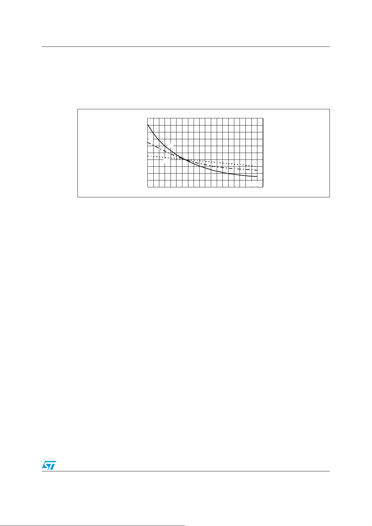
These parameters are specified at 25 °C and vary with the junction temperature as shown in
Figure 4. The I
, VGT and IL variations are the same for most devices, except for sensitive
GT
and low current SCRs (P0102BL, P01, X06, X02, X04 and TS420 series) and for ACS /
ACST devices.
Figure 4. Typical variations of the triggering gate current, the triggering gate
voltage and the latching current versus the junction temperature
I , V , I [T ] / I , V [T = 25 °C]
GT GT L j GT GT j,IL
I
L
I
GT
V
GT
T (°C)
C
Doc ID 17193 Rev 1 5/20
Page 6
AN3168 Triggering circuits
2 Triggering circuits
2.1 Two kind of power supply bias
To trigger a Triac, ACST, ACS or SCR, a gate current has to be applied on the gate pin and
circulates between gate and cathode (K) for SCR, or between gate and terminal A1 for Triac,
or between gate and terminal COM for ACST and ACS.
For non-insulated control circuits, this means that the reference of the control circuit has to
be related to K, A1 or COM. Then there are two ways to connect this drive reference.
● Solution 1: connect the control circuit ground (V
● Solution 2: connect the control circuit voltage supply (V
Solution 1 is called a positive power supply. The voltage supply V
drive reference (V
) which is connected to the mains terminal (line or neutral) as shown in
SS
Figure 5. If the supply is a 5 V power supply, then V
Figure 5. SCR / Triac control with positive power supply
) to K or A1
SS
) to A1 or COM
DD
is indeed above the
DD
is 5 V above the mains reference.
DD
+V
CONTROL
CONTROL
CONTROL
CIRCUIT
CIRCUIT
CIRCUIT
V
SS
DD
Vac
LOAD
LOAD
LOAD
A1
I
G
Solution 2 is called a negative power supply. The voltage supply reference (V
below A1 or COM, which is connected to the mains reference (line or neutral) as shown in
Figure 6. If the supply is a 5 V power supply, then V
This topology can be used with all Triacs, ACS and ACST, but not with SCR.
Figure 6. Triac and ACS / ACST control with negative power supply
Vac
LOAD
LOAD
2.2 Gate resistor value definition
The minimum gate current (IGT) required to trigger a Triac, SCR or ACS / ACST increases
as the junction temperature (T
equals the minimum ambient temperature. For appliance systems, the minimum ambient
temperature is generally 0 °C.
) decreases (see Figure 4). The worst case appears when Tj
j
Vac
A1 or COM
I
LOAD
LOAD
LOAD
I
G
K
SS
is 5 V below the line reference.
SS
+V
DD
CONTROL
CONTROL
CIRCUIT
G
CIRCUIT
V
SS
+V
DD
CONTROL
CONTROL
CONTROL
CIRCUIT
CIRCUIT
CIRCUIT
V
SS
) is indeed
For example, the ACS108-6Tx I
When T
equals 0 °C, IGT becomes 15 mA.
j
level is given as lower than 10 mA with Tj equals 25 °C.
GT
Doc ID 17193 Rev 1 6/20
Page 7

AN3168 Triggering circuits
In the following, we assume that the device gate is directly connected to a microcontroller
(MCU) output pin, through a gate resistor (R
To ensure that the MCU will always deliver “I
the value of the gate resistor (R
) must be calculated for the minimum available voltage.
G
).
G
(0 °C)”, the maximum gate current at 0 °C,
GT
This means that the minimum supply voltage and the maximum voltage drop of the gate
junction (V
) should be taken into account.
GT
The actual resistance value also depends on its tolerance. Typically, 1% precision resistors
are used. The microcontroller output port resistor (R
) maximum value also plays a role
DSon
in the current limitation.
The required value of R
is given in Equation 1.
G
Equation 1
VV
−
maxGTminDD
⋅+
GmaxDSon
Example: for a 20 mA output pin of a microcontroller, the worst R
01,1RR
()
C0I
°>
gt
could equal typically
DSon
50 Ω (ex: 1.5 V for 30 mA for an 85 °C junction temperature).
If an ACST6 is used, its I
the 10 mA given at 25 °C. V
decreases with a 2 mV/ °C rate. With a minimum supply voltage of 4.5 V and V
1.55 V (at 0 °C), R
is given in Equation 2 for ACST6 devices.
G
increases by 35% for a 0 °C junction temperature, compared to
GT
is given for Tj equals 25 °C. Its value increases as Tj
GT
equals
GT
Equation 2
−
< 16650
R
g
⋅
55,15,4
01,10135,0
Ω=−
The normalized value closest to 166 Ω is 165 Ω (1% precision resistor).
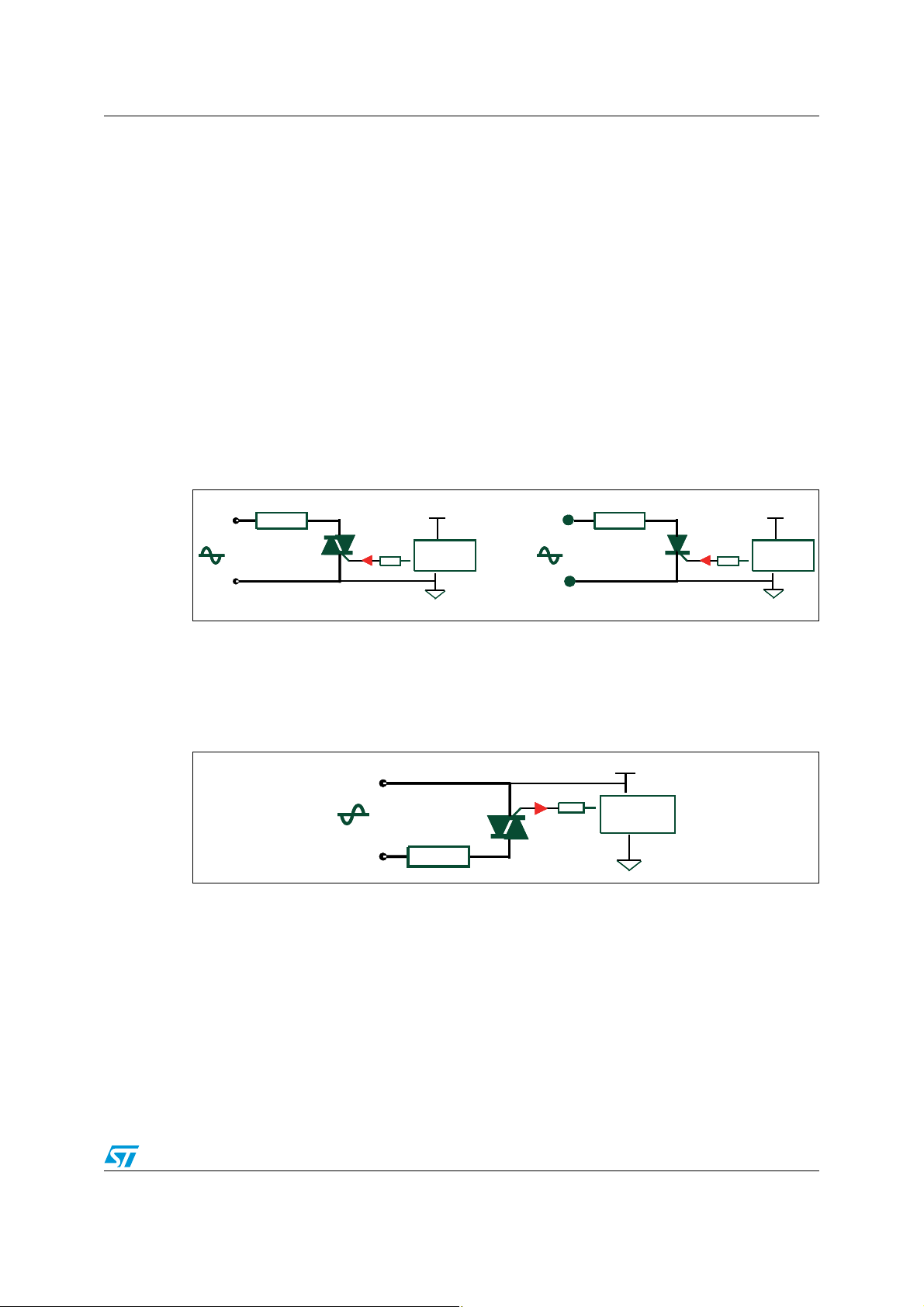
2.3 SCR and Triac triggering circuit with a positive power supply
With positive power supplies, the gate current can be only sourced from the control circuit to
the gate. Such a topology is adapted for SCRs control. For Triacs, the devices are then
triggered in quadrants Q1 and Q4. Such an operation is not advised for Triacs as the gate
current level is the highest for Q4 (see Section 1). Also Triac resistance to dI/dt at turn on is
lower for Q4.
As a control circuit designed with a positive power supply can be used only with standard
Triacs, the whole design has to be changed if the designer wants to switch from this
standard Triac to a snubberless or logic level Triac, or to an ACS or ACST. Indeed these
latter devices can not be triggered in Q4 (refer to Section 1).
When the gate current required to trigger the device is higher than the control-circuit output
current capability, the control-circuit output current has to be amplified. For example, today a
lot of MCUs feature output pins with a current capability around 30 mA. They can switch
Triacs safely with I
up to 15 to 20 mA. If a Triac with a 35 or 50 mA IGT has to be controlled
GT
by such an MCU, the two solutions are then:
● Use several MCU output pins in parallel (the best is to use a separate gate resistor
between each output pin and the Triac gate to ensure a good current repartition
between each pin).
● Use a bipolar transistor as shown in Figure 7.
Doc ID 17193 Rev 1 7/20
Page 8

AN3168 Triggering circuits
Figure 7. Gate current amplification with positive supply topology
+V
+V
DD
DD
LOAD
LOAD
CONTROL
Vac
Vac
T
T
I
G
CONTROL
CIRCUIT
CIRCUIT
V
V
SS
SS
With the bipolar solution, to keep the current sourced to the gate, the only way is then to use
a PNP transistor. A PNP transistor has to be used to set its drive reference to a stable bias,
which is the power supply (V
) in this case.
DD
This is another drawback of the positive power supply topology. To amplify the control circuit
output current, a PNP transistor has to be used instead of an NPN transistor. And a PNP
transistor has a lower current gain and a higher price than an NPN one.
2.4 Triac and ACS / ACST triggering circuit with negative power supply
Such a topology is the preferred one. The gate current is sunk from the gate by the control
circuit. The device then works in Q2 and Q3 quadrants. Such a topology is adapted for all
devices: standard, snubberless or logic level Triacs, and ACS or ACST.
For SCRs, the gate circuit has to be modified to source the current to the gate, as explained
in Section 2.5.
It should be noted that another advantage with this topology is that the control circuit output
current can be easily amplified if needed (see Section 2.3) with an NPN transistor as shown
in Figure 8.
Figure 8. Gate current amplification with negative supply topology
+V
Vac
LOAD
LOAD
I
G
CONTROL
CONTROL
CIRCUIT
CIRCUIT
DD
V
SS
Doc ID 17193 Rev 1 8/20
Page 9

AN3168 Triggering circuits
2.5 SCR triggering circuit with negative power supply
In the previous section, it has been demonstrated that choosing a negative power supply is
the best solution to control Triac or ACS / ACST. But in some applications, an electronic
circuit may have to control both Triac and SCR. And SCR can only be triggered by sourcing
a current to the gate.
Such applications are encountered when a switch has to control a DC load on the mains.
This occurs for example for some pumps used in coffee machines, which feature an internal
diode (see Figure 9). Also some magnetic door locks can be controlled only during one half
cycle. Then an SCR can be a cheaper solution than a Triac.
The circuit has then to be modified to allow the SCR to be triggered from a negative power
supply. The schematic in Figure 9 shows the addition of a PNP transistor (Q1), a low-voltage
diode (D1), a resistor (R2) and a capacitor (C1). This schematic is similar to the schematic
used to trigger Triacs with a positive power supply [see Reference 2].
The circuit operation is the following:
1. Q1 is OFF, C1 capacitor is charged thanks to D1 and R3.
2. Q1 is switched on by the “CTRL” signal, C1 capacitor is discharged through R2, the
SCR gate and Q1. A positive gate current pulse is then applied and the SCR switches
on.
C2 capacitor is used to increase the dV/dt immunity of X1 SCR, which is a very sensitive
device (I
The gate pulse width has to be set by the values of R2 and C1. The point is to keep the gate
current above max. I
latching current. For example, for the X00602, I
temperature.
< 200 µA for X00602 devices).
GT
up to the moment the anode current (IT) is above the maximum
GT
can reach up to 7 mA for a -20 °C junction
L
With the load used in this application, a gate current pulse width longer than 200 µs (t
required to reach 7 mA on I
. With the component values given in Figure 9, X1 gate current
T
remains above 2.4 mA during the whole “CTRL” pulse which lasts 400 µs (see Figure 10).
This allows correct operation even for very low ambient temperature operation.
Note: As gate current is very low, it can be estimated using the value of V
I
≈ (VD - 0.6 V) / R2
G
Figure 9. Drive schematic to trigger an SCR with a negative power supply
LOAD
R1
Vac
L1
D2
V
T
X1
X00602MA
I
I
T
T
C2
10n
R2
1k
R4
V
1k
D
5V
C1
470n
D1
D1N4448
PN2907
(see Figure 10),
D
R3
20k
V
R5
1k
CTRL
Q1
CTRL
p
) is
Doc ID 17193 Rev 1 9/20
Page 10

AN3168 Triggering circuits
Figure 10. Experimental validation of SCR triggering
I
A
(10mA/div)
V
D
(5V/div)
)
)
I X1 @L-20 ‹C 7 mA
-‹
V
CTRL
(10V/div)
)
V
T
(100V/div)
t
p
)
2.6 Diac control circuit
A Diac-based circuit can be used for non-insulated control circuits. Such a circuit is very
simple and known since the 70's. It was traditionally used for light dimmers or universal
motor speed-control circuits. Figure 11 gives the typical schematic for a light dimmer. L
C
are respectively the filter inductor and capacitor used to reduce the conducted
F
electromagnetic noise coming from Triac switch-on at voltage levels different from zero. The
circuit will be similar for a universal motor speed control circuit. The filter is then placed
before mains input as the noise comes mainly from motor brush commutations.
and
F
Figure 11. Diac-based light dimmer
Vac
I LAMP
R
L
F
C
F
T
D
Rs
P
V
V
BO
BO
DV
C
VC
DV
Vac
Vac
300 V/Div.
300 V/Div.
The operation of the dimmer circuit shown on Figure 11 is as follows:
1. The capacitor C is charged through the resistive potentiometer (P)
2. When V
decreased by
reaches the Diac breakover voltage (VBO), the Diac turns on and its voltage is
C
ΔV. Capacitor C is also discharged (ΔV reduction), this results in a
discharge current which is applied to the Triac gate. Rs is used to enlarge the gate
current pulse width. T is then switched on. Here, for the positive line polarity, T is
triggered in Q1.
3. T remains on until the next zero current crossing point. As T is on, there is no more high
voltage applied between A1 and A2, and the Diac is not charged anymore
Doc ID 17193 Rev 1 10/20
Page 11

AN3168 Triggering circuits
4. T Triac switches off when its current reaches zero. Then the mains voltage is applied
back between A1 and A2. So Capacitor C is then recharged in negative bias. This will
go on until the negative diac V
is reached.
BO
5. Triac T is switched on as explained on point 2 but here in Q3 (current sunk from the
gate and negative V
A2-A1
voltage).
This means that ACS can not be triggered by such circuits as they need that their gate
current is always sunk from the gate (i.e. only Q2 and Q3 triggering is possible).
The main point to check with Diac-based circuits is that the gate current pulse width lasts
enough time to allow the Triac anode current to reach the latching level I
(see Reference 1
L
for further information on this parameter). Figure 12 explains this point. The gate current has
to be higher than the maximum specified I
up to reaching a load current, i.e an anode
GT
current, higher than the maximum latching current (according to datasheet maximum value,
but also for the lowest junction temperature as I
increases with temperature decrease).
L
This will ensure a correct Triac turn on.
Figure 12. Required gate pulse width, with Diac circuit, to trigger the Triac
Load current
Load current
I
I
time
time
L MAX
time
time
Zoom
I
I
t
p
GT MAX
When the pulse width (t
Gate current
Gate current
) is defined, Figure 13 (from the DB3TG datasheet) can then be
p
used to define the Rs and C values. For example, if a 15 µs pulse width is required, a 33 Ω
resistor Rs is required with a 150 nF capacitor C.
It should be noted also that resistor Rs is helpful to keep Diac current below its maximum
repetitive current allowed (I
parameter).
TRM
Figure 13. Typical pulse width duration versus Rs and C values
15 µs
150 nF
Doc ID 17193 Rev 1 11/20
Page 12

AN3168 Examples of negative power supplies
3 Examples of negative power supplies
3.1 Linear power supply
The linear power supply is composed of a step down transformer, a diode bridge, a linear
regulator (U1) and some filtering capacitors (see Figure 14).
Figure 14. Linear power supply
V
DD
AC mains
T1
Diode Bridge
-+
U1
IN
OUT
C1 C2
V
DD
The output current (I
(V
) and the power factor (pf) of such a power supply. Due to the high mains current
DC
) depends on the power of the transformer (S), the output voltage
DC
GND
V
SS
harmonic content, a 0.5 power factor can usually be assumed. Without consideration of the
transformer, diodes and regulator power losses, the output current is then in Equation 3.
Equation 3
pfSI×
=
DC
V
DC
For a typical power factor of 0.5 and a 230 V / 15 V step down transformer, the calculated
output current capability and the measured typical standby power consumption (P
given according to the transformer power on Ta bl e 2 .
Table 2. Calculated output DC current and measured typical standby power
consumption
Transformer power, S 1.6 VA 3 VA 10 VA
Output DC current, I
DC
Stand-by power consumption, P
(measured) 0.08 W 0.5 W 1.1 W
OFF
53 mA 100 mA 333 mA
OFF
) are
The benefits of this solution are:
● High output current
● Possibility to easily generate multiple output voltages by using several secondary
windings
The drawbacks of this solution are:
● High cost
● High standby losses (due to the transformer magnetizing current)
● Bulky size of the 50 Hz transformer
Doc ID 17193 Rev 1 12/20
Page 13

AN3168 Examples of negative power supplies
3.2 Capacitive power supply
Figure 15 shows the schematic diagram of a capacitive negative power supply.
Figure 15. Capacitive power supply
V
DD
AC mains
D1
D2C2R1
To have a constant voltage across C1, the average value of the input current (I
equal to the average value of the output current (I
rectified current, whose average value (I
) is given in Equation 4 (R1 and C1
IN(av)
OUT(av)
). The input current is a half-wave
C1
V
SS
) must be
IN(av)
impedances and diode D2 voltage drop are neglected):
Equation 4
IV2Cf2I =×××=
)av(OUT)peak(mains)av(IN
The standby power consumption (P
current and the D1 zener voltage (V
) is set by the R1 resistor value, the average input
OFF
). The resistor R1 is required to limit the inrush current
Z
stress at power supply turn on and to avoid the overrating of the current protection of the
circuit. The standby power consumption is:
Equation 5
π
I(1RP ×+
2
××=
)av(INOFF
2
IV)
)av(INZ
For a 230 V / 50 Hz mains voltage, a 60 Ω resistor R1 (typical value) and a 15 V zener diode,
the calculated average output current and standby power consumption versus different AC
capacitors given in Ta bl e 3 .
Table 3. Calculated output DC current and measured typical standby power
consumption
AC capacitor, C2 220 nF 470 nF 680 nF 1 µF
Average output DC current, I
OUT(av)
Stand-by power consumption, P
OFF
7.1 mA 15.3 mA 22.1 mA 32.5 mA
0.12 W 0.3 W 0.48 W 0.8 W
The benefits of this solution are:
● Low cost (for output current lower than 20 mA)
● Small size
● Easy to implement
Doc ID 17193 Rev 1 13/20
Page 14

AN3168 Examples of negative power supplies
The drawbacks of this solution are:
● Low average output current. The maximum average output current is about 30 mA. For
higher output current, the size and the cost of the C2 capacitor becomes prohibitive.
Moreover, the inrush current stress at power supply turn on increases and will need
higher resistor R1 power.
● High standby power consumption. For example, the standby power consumption
equals about 0.8 W for a 230 V power supply with a capacitor C2 of 1 µF, a 15 V zener
diode and a 60 Ω R1.
3.3 Resistive power supply
Figure 16 show the schematic diagram of a negative resistive power supply.
Figure 16. Resistive power supply
V
DD
AC mains
R1 D1
D2
To have a constant voltage across C1, the average value of the input current (I
equal to the average value of the output current (I
OUT(av)
). The input current is a half-wave
C1
V
SS
) must be
IN(av)
rectified current, whose average value is given by the following equation (C1 impedance and
diode D1 voltage drop neglected):
Equation 6
VV
−
z)peak(mains
I =
=
)av(IN
1R
π×
The standby power consumption (P
I
)av(OUT
) is set by the R1 resistor value and is equal to:
OFF
Equation 7
2
)VV(
−
P
=
OFF
For a 230 V mains voltage and a 15 V zener voltage, the calculated average output current
and standby power consumption versus different resistors are:
Table 4. Calculated average output DC current and standby power consumption
Resistor R1 25 kΩ 18 kΩ 12 kΩ 8 kΩ
Average output DC current, I
Stand-by power consumption, P
z)peak(mains
1R4
×
OUT(av)
OFF
3.9 mA 5.5 mA 8.2 mA 12.3 mA
1 W1.3 W2 W 3 W
Doc ID 17193 Rev 1 14/20
Page 15

AN3168 Examples of negative power supplies
The benefits of this solution are:
● Low cost (for output currents < 10 mA)
● Small size
● Easy to implement
The drawbacks of this solution are:
● High resistor power dissipation. The resistor value is typically limited to 8 kΩ in order to
limit its power dissipation to 3 W.
● Low average output current. The maximum average output current for such supplies is
about 12 mA. For higher output current, the cost and the power dissipated by R1
becomes prohibitive.
● Stand-by power consumption. For an 8 kΩ resistor, a 15 V zener diode and 230 V
mains voltage, the standby power consumption is about 3 W.
3.4 Buck-boost power supply
The first example of switched mode power supplies (SMPS) that can be used to convert AC
mains voltage to DC voltage is the buck-boost converter. The buck-boost converter is the
simplest converter to implement a negative power supply. It should be noted that only
positive power supply can be implemented with a buck converter.
Figure 17 show the schematic diagram of a buck-boost negative power supply using
VIPer16 device.
Figure 17. Buck-boost power supply with VIPer16 device
D1
D2
R1
FB
V
dd
AC mains
COMP
Control
LIM
R5
D3
C4 C5
L1
D
S / GND
VIPer16
R3 R4
C1
C3
C2
R2
V
D4
L2
SS
C6
V
DD
When the VIPer MOSFET is on, the energy is stored in the inductance L2. When the VIPer
MOSFET is switched off, the energy stored during on time is supplied to the output capacitor
C6.
The input voltage is a half-wave rectified and filtered signal from diode D3 and filter PI (C4,
C5 and L1). The input voltage is close to the peak mains voltage, so close to 325 V for a 230
V mains. As the input voltage is much higher than the output voltage (typically 3.3 V, 5 V or
15 V), the switching duty cycle is very low (few %). Thanks to the VIPer integrated regulator,
a low duty cycle does not significantly affect operation. The buck-boost converter typically
Doc ID 17193 Rev 1 15/20
Page 16

AN3168 Examples of negative power supplies
operates in discontinuous mode. Discontinuous mode has the advantage of reducing the
size and the cost of the inductance with respect to continuous mode.
Equation 8 gives a simplified relation between the average output DC current and the
inductance value for discontinuous mode (VIPer power losses not considered).
Equation 8
2
)peak(mains
Vf2L2
×××
OUT
I
OUT
2
V
×α
=
The minimum inductance value is limited by the VIPer peak current limitation (I
Dlim
). For
VIPer16 device, the typical peak current limitation is 400 mA. The minimum inductance in
discontinuous mode is given by:
Equation 9
(min)
V
=
2L
The ratio between output and input voltages is used to define the VIPer duty cycle.
α×
)peak(mains
fI
×
limD
Equation 10
α
V
s
=
e
so
α−
1V
For a 230 V mains voltage, a 12 V output voltage and a 60 kHz switching frequency
(VIPer16 typical frequency), the average output current versus different inductances and the
typical standby power consumption are:
Table 5. Calculated average output DC current (
losses
L2 inductance 900 µH 800 µH 700 µH 600 µH (min. value)
Average output DC current, I
Stand-by power consumption, P
s
=α
VVV+
es
≈ 0.035) and typical standby
OUT(av)
OFF
100 mA 115 mA 130 mA 155 mA
≈ 100 mW
The advantage of a buck-boost converter compared to a buck converter is that there is no
need for an added output load resistance or output Zener (see Reference 3). For both
topologies, the feedback capacitor is still discharged with the IC feedback pin current,
whereas the output capacitor is not discharged if the output current is zero. The feedback
capacitor then indicates a lower output level than reality. Furthermore, this drawback is
amplified by the buck topology as the output capacitor is charged during each MOSFET on
time, whereas the feedback capacitor is not. So output voltage can increase to an excessive
value and has to be clamped.
The added resistance or clamping diode is then required at the buck output to avoid an
excessive output voltage in case of no-load or very light load.
With a buck-boost converter, the output capacitor is not charged during MOSFET on time.
Furthermore, the output voltage capacitor (C6) can not be charged if the feedback capacitor
(C2) voltage is lower than C6, as diode D2 is blocked. So there is no risk of an excessive
output voltage and the clamping device is not required.
Doc ID 17193 Rev 1 16/20
Page 17

AN3168 Examples of negative power supplies
For a buck-boost converter the efficiency (as well as the maximum output current) should be
lower and the output capacitor bigger than for a buck converter, as the whole inductor
current is used to charge the output capacitor for the buck converter. But for 230 V AC / 12 V
DC, the duty cycle is very low so there is no great difference between buck and buck-boost
performances. Similar efficiency is reached for both topologies, with the same reactive
components.
3.5 Flyback power supply
The second SMPS topology widely used today by designers is the flyback topology. This
converter uses a transformer to store the energy instead of an inductance. The benefit of
this solution, compared to a buck-boost converter, is the possibility to insulate the output
voltage and also to generate several output voltages by using several secondary windings. A
flyback converter can also deliver a higher power with the same monolithic device (VIPer)
compared to a buck or buck-boost converter.
For AC switch control, as the V
level has to be connected to the mains, there is no interest
DD
in implementing an insulated power supply. So only the advantage of implementing a 2nd
low-voltage supply will push designers to use such a topology. Note that this 2nd supply can
then be insulated from the mains.
It is easy to implement a negative supply with a flyback converter, and the output voltage is
insulated from the mains. So the V
line. The V
voltage is then no longer insulated from the mains. This means that the
DD
terminal can either be connected to the neutral or the
DD
insulation has to be implemented elsewhere to protect the appliance user from electrical
shocks (for example, with an insulated keyboard and display).
Note also that due to the transformer ratio, a flyback converter can work with a higher duty
cycle than a buck-boost converter. The input peak current is then lower with a flyback
converter than with a buck-boost converter. The MOSFET peak current is thus lower and so
are its switching losses. The flyback converter efficiency can then be slightly better.
As for buck-boost converter, the VIPer operates in discontinuous mode.
The drawback of the flyback solution is that the transformer used most of the time is a
specific device, whereas a standard inductance can be used with a buck-boost converter.
Consequently, the flyback converter cost could be higher by about 15% than the buck-boost
converter cost for the same output power.
Figure 18 shows the schematic diagram of a flyback power supply using a VIPer16 device.
For a 230 V mains voltage and a 5 V output voltage, the standby power consumption is
typically around 70 mW with this circuit.
Doc ID 17193 Rev 1 17/20
Page 18

AN3168 Examples of negative power supplies
Figure 18. Flyback power supply with VIPer16 device
R6
D6
R1
V
DD
C6
C6
V
SS
AC mains
AC mains
COMP
FB
Q1
D5
C1 R2
Vdd
Control
LIM
VDD
V
DD
Vdd
Vdd
S / GND
C4 C5
C4 C5
D3
R3
D3
R3
L1
L1
VIPer16
VIPer16
D
D
D1
D2
C1
C2
C2
R7
R7
D4
D4
Q1
D5
R5
R4
C3
C3
For flyback converter design, please refer to the technical note TN0023 from
STMicroelectronics.
3.6 Comparison of negative power supplies
Ta bl e 6 summarizes the advantages and drawbacks of the negative power supplies
introduced in the point 3 according to the cost, the size, the easiness of implementation, the
standby power consumption, the output current capability and the capability to generate
easily one or more output voltages.
Table 6. Comparison of negative power supplies
Powe r supply
type
Cost Size
Easy of
implementation
Linear - -- ++ -- + 1 or more
Capacitive + - ++ - -- 1
Resistive - + ++ -- --- 1
Buck-boost ++ ++ + +++ +++ 1
Flyback + + + +++ ++++ 1 or more
1. Key: +: good, -: bad
(1)
Standby power
consumption
Output
Max. current
level
Number
Doc ID 17193 Rev 1 18/20
Page 19

AN3168 Conclusion
4 Conclusion
This application note has presented circuits that can be used to control SCR, Triacs or
ACS / ACST devices, as far as a non-insulated circuit is allowed.
It has been shown that a negative power supply is the best topology as it can be used for all
AC switches. Moreover if an SCR has to be controlled with a board using a negative supply
to trigger AC switches, a simple schematic has been presented to control the SCR with the
same supply.
Schematics for negative switched mode power supplies have been presented.
Even if the first reflex of a designer is to implement a positive power supply, negative power
supplies are as easy to implement as positive ones. There are also some benefits with a
negative supply topology such as, for example, the removal of output overvoltage protection
for non-insulated SMPS (buck-boost topology compared to buck topology), optotransistor
removal (for flyback converters) and the use of NPN transistors instead of PNP to amplify
the gate current.
5 References
1. “Latching current”, Application note AN303, STMicroelectronics.
2. “QII and QIII Triac triggering with positive power supply”, Application note AN440,
STMicroelectronics.
3. “VIPower: Low Cost Power Supplies Using VIPer12A in Non Isolated Applications”, N.
Aiello - F. Gennaro - R. Santori, Application note AN1357, STMicroelectronics, 2001.
4. “Discontinuous Flyback transformer description and design parameters”, Technical
note TN0023, STMicroelectronics.
6 Revision history
Table 7. Document revision history
Date Revision Changes
09-Mar-2010 1 Initial release.
Doc ID 17193 Rev 1 19/20
Page 20

AN3168
Please Read Carefully:
Information in this document is provided solely in connection with ST products. STMicroelectronics NV and its subsidiaries (“ST”) reserve the
right to make changes, corrections, modifications or improvements, to this document, and the products and services described herein at any
time, without notice.
All ST products are sold pursuant to ST’s terms and conditions of sale.
Purchasers are solely responsible for the choice, selection and use of the ST products and services described herein, and ST assumes no
liability whatsoever relating to the choice, selection or use of the ST products and services described herein.
No license, express or implied, by estoppel or otherwise, to any intellectual property rights is granted under this document. If any part of this
document refers to any third party products or services it shall not be deemed a license grant by ST for the use of such third party products
or services, or any intellectual property contained therein or considered as a warranty covering the use in any manner whatsoever of such
third party products or services or any intellectual property contained therein.
UNLESS OTHERWISE SET FORTH IN ST’S TERMS AND CONDITIONS OF SALE ST DISCLAIMS ANY EXPRESS OR IMPLIED
WARRANTY WITH RESPECT TO THE USE AND/OR SALE OF ST PRODUCTS INCLUDING WITHOUT LIMITATION IMPLIED
WARRANTIES OF MERCHANTABILITY, FITNESS FOR A PARTICULAR PURPOSE (AND THEIR EQUIVALENTS UNDER THE LAWS
OF ANY JURISDICTION), OR INFRINGEMENT OF ANY PATENT, COPYRIGHT OR OTHER INTELLECTUAL PROPERTY RIGHT.
UNLESS EXPRESSLY APPROVED IN WRITING BY AN AUTHORIZED ST REPRESENTATIVE, ST PRODUCTS ARE NOT
RECOMMENDED, AUTHORIZED OR WARRANTED FOR USE IN MILITARY, AIR CRAFT, SPACE, LIFE SAVING, OR LIFE SUSTAINING
APPLICATIONS, NOR IN PRODUCTS OR SYSTEMS WHERE FAILURE OR MALFUNCTION MAY RESULT IN PERSONAL INJURY,
DEATH, OR SEVERE PROPERTY OR ENVIRONMENTAL DAMAGE. ST PRODUCTS WHICH ARE NOT SPECIFIED AS "AUTOMOTIVE
GRADE" MAY ONLY BE USED IN AUTOMOTIVE APPLICATIONS AT USER’S OWN RISK.
Resale of ST products with provisions different from the statements and/or technical features set forth in this document shall immediately void
any warranty granted by ST for the ST product or service described herein and shall not create or extend in any manner whatsoever, any
liability of ST.
ST and the ST logo are trademarks or registered trademarks of ST in various countries.
Information in this document supersedes and replaces all information previously supplied.
The ST logo is a registered trademark of STMicroelectronics. All other names are the property of their respective owners.
© 2010 STMicroelectronics - All rights reserved
STMicroelectronics group of companies
Australia - Belgium - Brazil - Canada - China - Czech Republic - Finland - France - Germany - Hong Kong - India - Israel - Italy - Japan -
Malaysia - Malta - Morocco - Philippines - Singapore - Spain - Sweden - Switzerland - United Kingdom - United States of America
www.st.com
Doc ID 17193 Rev 1 20/20
 Loading...