

Page 1

AN3161
Application note
Using the STGW35HF60WD advanced PT IGBT in parallel
Introduction
When two or more IGBTs are connected in parallel to improve the total efficiency in high
output power systems, special care is required to ensure that current sharing between the
devices is as equal as possible. Current sharing is mainly influenced by differences in IGBT
static parameters, circuitry layout (both driving and power) and thermal imbalances. All of
these elements must be considered, especially when PT (punch-through) IGBTs work in
parallel, due to their negativ e V
to the market while supporting reliable and easier paralleling for higher power level
applications, ST offers the STGW35HF60WD 35 A, 600 V ultra fast IGBT with V
selection. This device is explained in greater detail in Section 3: New advanced planar PT
STGW35HF60WD.
coefficient. In order to pro vide the m ost efficien t IGBT
CE(sat)
CE(sat)
May 2010 Doc ID 17151 Rev 1 1/14
www.st.com
Page 2

Contents AN3161
Contents
1 Saturation voltage impact on parallel . . . . . . . . . . . . . . . . . . . . . . . . . . . 4
1.1 PT, NPT and trench field stop . . . . . . . . . . . . . . . . . . . . . . . . . . . . . . . . . . . 4
2 General guidelines on paralleling . . . . . . . . . . . . . . . . . . . . . . . . . . . . . . 6
2.1 Thermal system impact . . . . . . . . . . . . . . . . . . . . . . . . . . . . . . . . . . . . . . . 6
2.2 Layout considerations . . . . . . . . . . . . . . . . . . . . . . . . . . . . . . . . . . . . . . . . . 6
3 New advanced planar PT STGW35HF60WD . . . . . . . . . . . . . . . . . . . . . . 7
3.1 Notes on technology and V
3.2 E
impact on parallel . . . . . . . . . . . . . . . . . . . . . . . . . . . . . . . . . . . . . . . 8
OFF
grouping . . . . . . . . . . . . . . . . . . . . . . . . 7
CE(sat)
4 The STGW35HF60WD on the test bench . . . . . . . . . . . . . . . . . . . . . . . . . 9
5 Conclusion . . . . . . . . . . . . . . . . . . . . . . . . . . . . . . . . . . . . . . . . . . . . . . . . 12
6 Revision history . . . . . . . . . . . . . . . . . . . . . . . . . . . . . . . . . . . . . . . . . . . 13
2/14 Doc ID 17151 Rev 1
Page 3

AN3161 List of figures
List of figures
Figure 1. ∆IC (@TJ = 25 °C) of two paralleled IGBT . . . . . . . . . . . . . . . . . . . . . . . . . . . . . . . . . . . . . . 4
Figure 2. ∆I
Figure 3. Static V
Figure 4. E
Figure 5. DC-DC boost scheme . . . . . . . . . . . . . . . . . . . . . . . . . . . . . . . . . . . . . . . . . . . . . . . . . . . . . 9
Figure 6. V
Figure 7. ∆I
Figure 8. ∆I
Figure 9. ∆I
Figure 10. ∆I
Figure 11. ∆I
Figure 12. ∆I
(@TJ > 25 °C) of two paralleled IGBT without negative feedback . . . . . . . . . . . . . . . . . 5
C
vs. V
OFF
CE(sat)
at TC = 25 °C (board startup) . . . . . . . . . . . . . . . . . . . . . . . . . . . . . . . . . . . . . . . . . . . . 10
C
at TC = 100 °C . . . . . . . . . . . . . . . . . . . . . . . . . . . . . . . . . . . . . . . . . . . . . . . . . . . . . . . 10
C
at TC = 25 °C (board startup) . . . . . . . . . . . . . . . . . . . . . . . . . . . . . . . . . . . . . . . . . . . . 11
C
at TC = 100 °C . . . . . . . . . . . . . . . . . . . . . . . . . . . . . . . . . . . . . . . . . . . . . . . . . . . . . . . 11
C
at TC = 25 °C (board startup) . . . . . . . . . . . . . . . . . . . . . . . . . . . . . . . . . . . . . . . . . . . . 11
C
at TC = 100 °C . . . . . . . . . . . . . . . . . . . . . . . . . . . . . . . . . . . . . . . . . . . . . . . . . . . . . . . 11
C
(@20 A,15 V) derating for STGW35HF60WD . . . . . . . . . . . . . . . . . . . . . . . . 7
CE(sat)
for the STGW35HF60WD . . . . . . . . . . . . . . . . . . . . . . . . . . . . . . . . . . . . . 8
CE(sat)
(@20 A, 25 °C, 15 V) grouping for the STGW35HF60WD. . . . . . . . . . . . . . . . . . . . 9
Doc ID 17151 Rev 1 3/14
Page 4
Saturation voltage impact on parallel AN3161
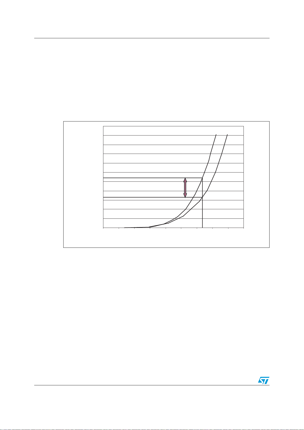
1 Saturation voltage impact on parallel
1.1 PT, NPT and trench field stop
PT IGBTs (including those offered by STMicroelectronics) have typically negative V
CE(sat)
coefficients at current operative levels. This has a very important effect when two devices
work in parallel. Due to their difference in static output characteristics, the one with the
lowest static V
carries more current than the other, as shown in Figure 1. The ∆IC is
CE(sat)
the static current difference established at the beginning.
Figure 1. ∆I
(@TJ = 25 °C) of two paralleled IGBT
C
I
CTOT=IC1+IC2
I
C1
ΔI
C
I
C2
collector current ( A )
c
I
V
CE1=VCE2
0 0.25 0.5 0.75 1 1.25 1.5 1.75 2 2.25
Vce
collector emitter voltage (V)
Assuming the same T
power than the other, and its T
at the beginning, the IGBT carrying higher current dissipates more
J
increases. As a consequence, its V
J
the current of the IGBT in crea ses further. The IGBT carrying less current a lso d ecre ases its
static V
as a consequence of the common VCE, and its current must satisfy the
CE(sat)
following equation:
Equation 1
I
CTOTIC1 T1()IC2 T2()
4/14 Doc ID 17151 Rev 1
AM06441v1
decreases and
CE(sat)
+=
Page 5
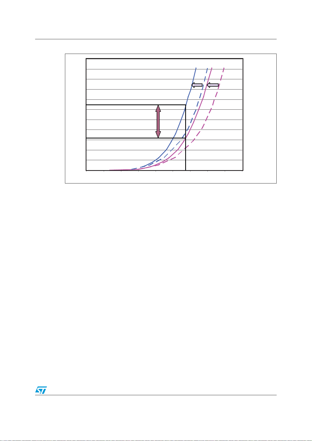
AN3161 Saturation voltage impact on parallel
Figure 2. ∆IC (@TJ > 25 °C) of two paralleled IGBT without negative feedback
Tj>25°C,
=15V
V
I
CTOT=IC(T1)+IC(T2)
I
C2
ΔI
C
collect or current (A)
c
I
I
C1
V
CE1=VCE2
GE
0 0.25 0.5 0.75 1 1.25
Vce collect or em i t t er vol t age ( V)
As a consequence of the negativ e V
1.5
coefficient, a higher ∆IC is established at high TJ
CE(sat)
1.75 2
2.25
AM06440v1
(Figure 2). This can cause thermal instability if an accurate negative feedback is not
implemented. NPT and field stop IGBTs have positive V
coefficients (the latter
CE(sat)
typically starting from low current levels). When working in parallel the one carrying the
higher current increases its temperature , which causes a V
increase. This means that,
CE(sat)
at the same on-state voltage level, the current does not increase with temperature as in PT
IGBTs; this guarantees an intrinsic balancing mechanism, preventing thermal runaway.
Doc ID 17151 Rev 1 5/14
Page 6

General guidelines on paralleling AN3161
2 General guidelines on paralleling
2.1 Thermal system impact
In order to guarantee the satisfactory performance of paralleled de vices, regardless of the
IGBT technology used, it is recommended to place them on the same heatsink, very close
together. If the IGBTs are sufficiently close, the one with the higher T
improving temperature and current sharing. PT IGBTs in particular benefit from the common
heatsink, as it balances the negative V
the thermal system impact is considered on paralleling, the mutual thermal resistance
between the two junction s is th e most important fa ctor impact ing on the dynamic ∆I
temperatures. If a thin laye r of silicon grease is used between the IGBT case and the
heatsink, power sharing greatly improves, leading to a significant ∆I
temperatures. This occurs because the silicon grease significantly decreases the thermal
resistance between the relative junctions.
2.2 Layout considerations
General rules during the design phase should be adopted to minimize unavoidable
asymmetries occurring under transient conditions (turn-on and turn-off). First, it is
recommended to make the gate drive circuit as symmetrical as possible, and to use
individual gate resistors. Individual driving stages provide two advantages:
● They avoid imbalances during the turn-on and turn-off phase. They mainly occur when
the two IGBTs have different V
common gate. As a consequence, o ne of th e t w o I GBTs turns on before the other, and
turns off later.
● They damp oscillations during the tr ansient state, caused by the cross-capa citive
coupling of the paralleled devices with the driving loop inductances. If parasitic
oscillations are still present due to layout inductances, f errite beads added to each gate
wire can help to drastically reduce the oscillations.
coefficient, which prevents thermal runway. If
CE(sat)
values and the same forced VGE due to the
plateau
will heat its neighbor,
J
at high
C
reduction at operating
C
Additionally, voltage overshoot can appear across the devices due to the di/dt and to stray
inductances in the power circuit. It is suggeste d to mak e th ese loop inductance s as short as
possible in order not to exceed the absolute maximum rating of the IGBT voltage, rather
than make them symmetrical. If not perfectly matched, the collector and emitter inductances
can cause different current slopes during switch-off. Any IGBT technology can benefit from
this layout optimization.
6/14 Doc ID 17151 Rev 1
Page 7
AN3161 New advanced planar PT STGW35HF60WD
3 New advanced planar PT STGW35HF60WD
3.1 Notes on technology and V
An advanced PT IGBT has been introduced to enhance the previous 600 V, 35 A IGBT
STGW35NC60WD, tailored for high-frequency applications. From a technology point of
view, two main improvements have been implemented on this IGBT:
1. The innovative double-drift process which changed the doping profile
2. The advanced planar strip layout
Both factors allow the reduction of the effective resistance in the drift (N ¯) region and
significantly improve the dynamic performance, especially at high temperature. The
changes performed on the horizontal a nd vertical structure and their effect on this IGBT are
clearly shown in its datasheet: the new STGW35HF60WD shows a lower V
value than the equivalent STGW35NC60WD, and its E
T
= 125 °C) is guaranteed as per the datasheet. Tests performed on a significant n umber of
J
STGW35HF60WD samples show that the static temperature coefficient (see Equation 2),
changes in relation to the absolute V
Equation 2
V
CE sat()TJ
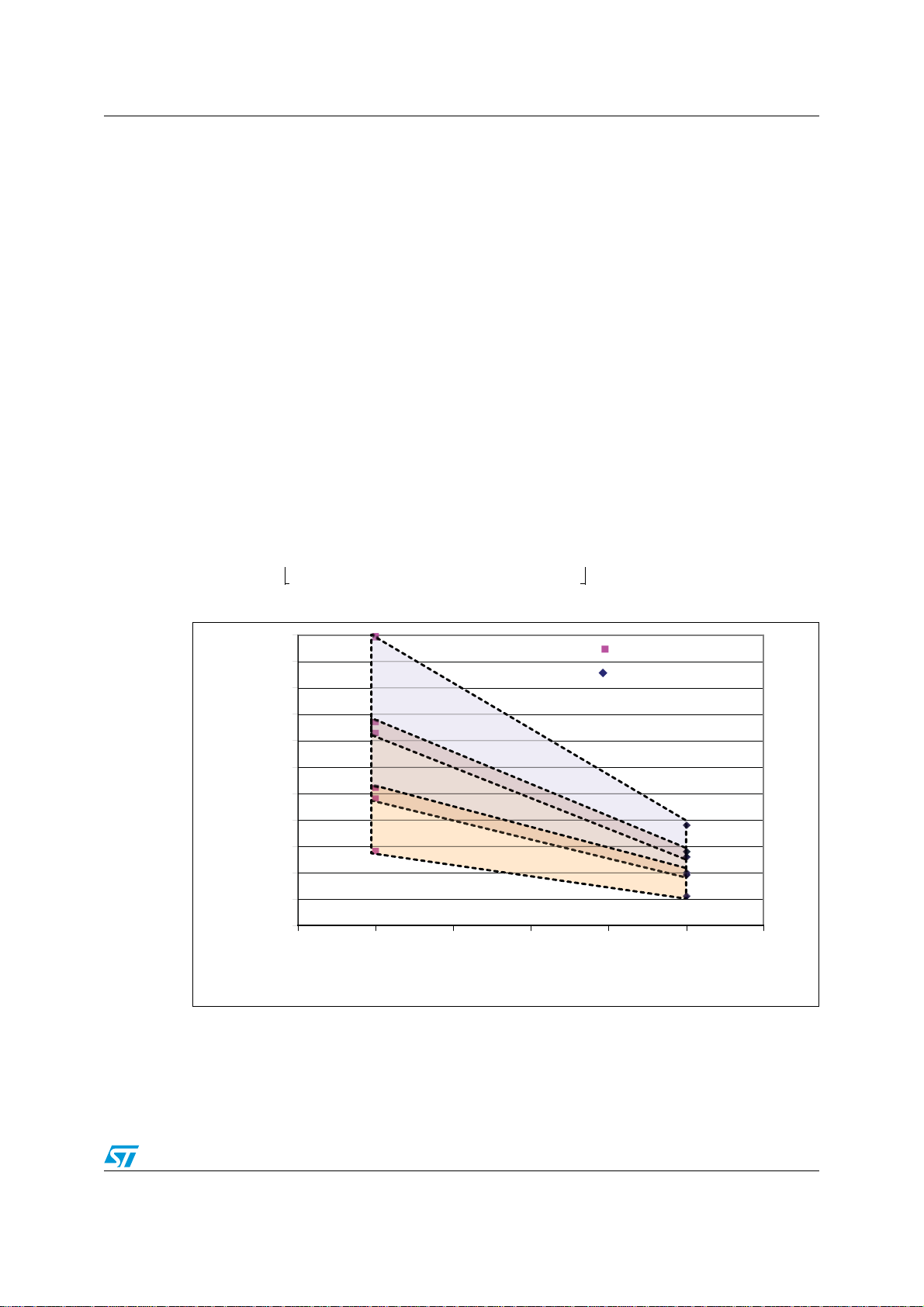
Figure 3. Static V
CE(sat)
25° C=()V
(@20 A,15 V) derating for STGW35HF60WD
2.5
GROUP
"C"
2.4
Δ≈15.5%
2.3
CE(sat)
CE sat()TJ
CE(sat)
grouping
max value (at IC = 20 A,
off
value, as shown in Figure 3.
125°C=()–⋅ V
CE sat()TJ
V
CE(sat)
V
CE(sat)
CE(sat)
125° C=()⁄
at 20 A, 25 °C
at 20 A, 125 °C
typical
2.2
(V)
CESAT
V
2.1
2
1.9
1.8
GROUP
"B"
Δ≈14.3%
GROUP
"A"
Δ≈13%
1.7
Δ≈ 6%
1.6
1.5
1.4
0 25 50 75 100 125 150
Tj ( ° C)
AM06442v1
Figure 3 also explains how the total V
balanced and reliable paralleling. The ∆ symbol beside group A, whose V
belong to the interval (1.68 V
− 1.92 V [@20 A, 25 °C]), satisfies the equation:
Doc ID 17151 Rev 1 7/14
population has been split to guarantee well-
CE(sat)
CE(sat)
values
Page 8

New advanced planar PT STGW35HF60WD A N31 6 1
Equation 3
The same equation can be written for groups B and C. From Figure 3 it is clear that each
group has been chosen with a specific ∆ value at T
at T
balancing mechanism helps to keep a very low and stable ∆I
the same group work in parallel.
3.2 E
It is well known that the E
cannot be neglected. This impact becomes significant when high T
are considered. The STGW35HF60WD guarantees that the E
controlled and that its value is in the range of 80%
worst thermal derating (
derating (
Figure 4. E
∆ MaxValue MinValue–()MaxValue MinValue+()⁄ 2⁄= 13=
= 25 °C. Despite the original imbalance
, the ∆ of each group moves towards the same value at high temperature. This
AMB
impact on parallel
OFF
contribution of IGBTs on high-frequency DC-DC conversion
OFF
∼ 110%), while high V
J
when two or more IGBTs of
C
and high current levels
J
thermal derating can be
−110%. Low V
samples have the lowest thermal
CE(sat)
OFF
samples show the
CE(sat)
∼ 80%), which is clearly illustrated in Figure 4.
450
400
350
OFF
vs. V
for the STGW35HF60WD
CE(sat)
Vcl=390V, Ic =20A, Rg=10 ohm , VGE=15V
%
300
250
Eoff (µJ)
200
150
100
1.3 1 .4 1.5 1 .6 1 .7 1.8 1.9 2.0 2.1 2.2 2.3 2.4 2.5 2.6
V
(V)
CESAT
The difference in E
Tj=25°C Tj=125°C
derating has been considered on the V
OFF
selection, and also
CE(sat)
AM06443v1
explains why the selected groups have different widths.
8/14 Doc ID 17151 Rev 1
Page 9

AN3161 The STGW35HF60WD on the test bench
4 The STGW35HF60WD on the test bench
A DC-DC boost converter (Figure 5) has been used as a test vehicle to evaluate two
STGW35HF60WD IGBTs working in parallel.
Figure 5. DC-DC boost scheme
Boost specifications:
–V
–I
–V
IN(DC)
TAV
OUT
= 250 V
= 20 A
= 380 V
–Fsw = 30 kHz
– Duty = 0.33%
– CCM operation
A preliminary analysis has been performed to measure the dynamic ∆IC established
between several couples of paralleled IGBTs. To target the best current sharing, the static
V
(@20 A,15 V, 25 °C) has been chosen as selection criteria to split the total IGBT
CE(sat)
population (as illustrated in Figure 6) and three sets of tests are reported in this document.
Figure 6. V
(@20 A, 25 °C, 15 V) grouping for the STGW35HF60WD
CE(sat)
Doc ID 17151 Rev 1 9/14
Page 10

The STGW35HF60WD on the test bench AN3161
Couple n.1 and n.3 tested have ∆V
example, couple n.1, has been chosen with ∆V
mV for group A) in order to guarantee a more reliable result in terms of ∆I
@20 A, 25 °C different from its relative group. For
CE(sat)
= 270 mV (wider than ∆V
CE(sat)
. The same
C
CE(sat)
= 200
consideration applies for couple n.3.
● Couple n.1
– device n.1: V
– device n.2: V
∆V
● Couple n.2
CE(sat)
= 270 mV
– device n.1: V
– device n.2: V
∆V
● Couple n.3
CE(sat)
= 250 mV
– device n.1: V
– device n.2: V
∆V
CE(sat)
= 400 mV
The goal of the on-board tests was to evaluate how the dynamic ∆I
from board startup (T
= 25 °C) to a steady-state condition in terms of thermal sharing (TC =
C
= 1.75 V (@20 A, 25 °C,15 V)
CE(sat)
t = 2.02 V (@20 A, 25 °C, 15 V)
CE(sat)
= 1.84 V (@20 A, 25 °C,15 V)
CE(sat)
= 2.09 V (@20 A, 25 °C, 15 V)
CE(sat)
= 1.94 V (@20 A, 25 °C,15 V)
CE(sat)
= 2.34 V (@20 A, 25 °C, 15 V)
CE(sat)
of each group moves
C
100 °C). After board startup, the two paralleled devices share the total power, taking
advantage of the common heatsink and layout optimization (as suggested in Section 2.1
and Section 2.2). Thanks to the negative thermal feedback introduced by the common
heatsink, the dynamic ∆I
stable even at high T
decreases despite of its initial value of TC = 25 °C, and remains
C
temperatures.
J
Couple n.1
Figure 7. ∆IC at TC = 25 °C (board startup) Figure 8. ∆IC at TC = 100 °C
10/14 Doc ID 17151 Rev 1
Page 11

AN3161 The STGW35HF60WD on the test bench
Couple n.2
Figure 9. ∆I
at TC = 25 °C (board startup) Figure 10. ∆IC at TC = 100 °C
C
Couple n.3
Figure 11. ∆IC at TC = 25 °C (board startup) Figure 12. ∆IC at TC = 100 °C
Table 1. ∆IC/I
(25 °C)/I
∆I
C
∆I
(100 °C)/I
C
If an acceptable value of ∆IC/I
shows that three V
TOT
TOT
% summary
TOT
(∆V
Couple 1
CE(sat)
= 270 mV)
(∆V
Couple 2
CE(sat)
= 250 mV)
(∆V
Couple 3
CE(sat)
= 400 mV)
% 20% 21% 25.4%
% 14% 12.9% 11%
= 10% −14% is considered in terms of efficiency, Table 1
TOT
grouping allows the paralleling o f t he IGBTs with excellent
CE(sat)
performance results.
Doc ID 17151 Rev 1 11/14
Page 12
Conclusion AN3161
5 Conclusion
Several tests performed on the new advanced planar PT STGW35HF60WD show that
STMicroelectronics’ advanced PT technology can be paralleled with satisfactory
performance in terms of thermal and current sharing. Reliable parallelin g, how e v er, requires
good thermal feedback implementation and V
Both of these factors provide a balancing mechanism to reduce and keep stable the
dynamic ∆I
different V
at operating conditions. Finally, the STGW35HF60WD is offered in three
C
groups, as shown in Table 2: Suggested V
CE(sat)
selection as per datasheet and as reported in the datasheet, for a safe parallel connection
without risk of thermal runaway.
selection of the total IGBT population.
CE(sat)
(@20 A, 25 °C, 15 V)
CE(sat)
Table 2. Suggested V
CE(sat)
(@20 A, 25 °C, 15 V) selection as per datasheet
Group “A” Group “B” Group “C”
1.68 V
− 1.92 V 1.88 V − 2.17 V 2.13 V − 2.5 V
@20 A, 25 °C, 15 V @20 A, 25 °C, 15 V @20 A, 25 °C, 15 V
1. The V
testing rules.
grouping reported above is slightly different from the one in Figure 6, in order to meet the
CE(sat)
(1)
12/14 Doc ID 17151 Rev 1
Page 13

AN3161 Revision history
6 Revision history
Table 3. Document revision history
Date Revision Changes
05-May-2010 1 Initial release.
Doc ID 17151 Rev 1 13/14
Page 14

AN3161
Please Read Carefully:
Information in this document is provided solely in connection with ST products. STMicroelectronics NV and its subsidiaries (“ST”) reserve the
right to make changes, corrections, modifications or improvements, to this document, and the products and services described herein at any
time, without notice.
All ST products are sold pursuant to ST’s terms and conditions of sal e.
Purchasers are solely res ponsibl e fo r the c hoic e, se lecti on an d use o f the S T prod ucts and s ervi ces d escr ibed he rein , and ST as sumes no
liability whatsoever relati ng to the choice, selection or use of the ST products and services described herein.
No license, express or implied, by estoppel or otherwise, to any intellectual property rights is granted under this document. If any part of this
document refers to any third pa rty p ro duc ts or se rv ices it sh all n ot be deem ed a lice ns e gr ant by ST fo r t he use of su ch thi r d party products
or services, or any intellectua l property c ontained the rein or consi dered as a warr anty coverin g the use in any manner whats oever of suc h
third party products or servi ces or any intellectual property contained therein.
UNLESS OTHERWISE SET FORTH IN ST’S TERMS AND CONDITIONS OF SALE ST DISCLAIMS ANY EXPRESS OR IMPLIED
WARRANTY WITH RESPECT TO THE USE AND/OR SALE OF ST PRODUCTS INCLUDING WITHOUT LIMITATION IMPLIED
WARRANTIES OF MERCHANTABILITY, FITNESS FOR A PARTICUL AR PURPOS E (AND THEIR E QUIVALENTS UNDER THE LAWS
OF ANY JURISDICTION), OR INFRINGEMENT OF ANY PATENT, COPYRIGHT OR OTHER INTELLECTUAL PROPERTY RIGHT.
UNLESS EXPRESSLY APPROVED IN WRITING BY AN AUTHORIZED ST REPRESENTATIVE, ST PRODUCTS ARE NOT
RECOMMENDED, AUTHORIZED OR WARRANTED FOR USE IN MILITARY, AIR CRAFT, SPACE, LIFE SAVING, OR LIFE SUSTAINING
APPLICATIONS, NOR IN PRODUCTS OR SYSTEMS WHERE FAILURE OR MALFUNCTION MAY RESULT IN PERSONAL INJ URY,
DEATH, OR SEVERE PROPERTY OR ENVIRONMENTAL DAMAGE. ST PRODUCTS WHICH ARE NOT SPECIFIED AS "AUTOMOTIVE
GRADE" MAY ONLY BE USED IN AUTOMOTIVE APPLICATIONS AT USER’S OWN RISK.
Resale of ST products with provisions different from the statements and/or technical features set forth in this document shall immediately void
any warranty granted by ST fo r the ST pro duct or serv ice describe d herein and shall not cr eate or exten d in any manne r whatsoever , any
liability of ST.
ST and the ST logo are trademarks or registered trademarks of ST in various countries.
Information in this document su persedes and replaces all info rmation previously supplied .
The ST logo is a registered trademark of STMicroelectronics. All other names are the property of their respective owners.
© 2010 STMicroelectronics - All rights reserved
STMicroelectronics group of compan ie s
Australia - Belgium - Brazil - Canada - China - Czech Republic - Finland - France - Germany - Hong Kong - India - Israel - Italy - Japan -
Malaysia - Malta - Morocco - Philip pines - Singapore - Spain - Sweden - Swit zerland - United Kingdom - United States of America
www.st.com
14/14 Doc ID 17151 Rev 1
 Loading...