

Page 1

AN3152
Application note
The right technology for solar converters
Introduction
Following a short overview of types of solar power systems and converters, this application
note introduces a fully working, grid-connected solar inverter prototype suitable for rooftop
applications. This solar inverter has been equipped with STMicroelectronics’ MDmesh™
and silicon carbide (SiC) devices to allow evaluation of these products in “green”
technologies.
Thanks to ST’s newest technologies (MDmesh™ V and SiC) and a new converter
philosophy, a 650 V fast power MOSFET can be used to boost performance and reduce the
size of the converter. A stage-by-stage explanation is presented here, as well as the
topologies adopted, and a detailed analysis of the front-end stage of the inverter is
discussed. The BOOST stage is used as a case study to validate the performance of the
new power MOSFETs and diodes.
Everyone is thinking “green’ these days. Adding to the new green conscience are the
increasing costs of fossil and nuclear fuels, prompting the market to turn to creative
technologies that use renewable resources to produce energy. Energy produced from
renewable resources are becoming an important contribution to the world’s total energy
demand and will increase in the next decades. Solar photovoltaic technology represents one
of the most promising energy resources, due to its low environmental impact and high
reliability. Every photovoltaic (PV) system consists of a module array and an inverter. The
inverter module is mandatory on all grid-connected applications, in order to amplify the low
DC voltage generated by the module to the higher AC level required by the grid. If several
modules are connected in series it might not be necessary to include amplification, but in
any case a maximum power point tracking (MPPT) function is required.
This prototype has a wide operating input voltage range (from 200 V to 400 V), and 3 kW of
maximum power output, since it is intended for rooftop applications. Total efficiency must be
at least 97%, and an MPPT function is implemented in order to enable panels to work at
their highest efficiency. In fact, the PV module (or modules, if connected in series) changes
its maximum power point continually during normal operation due to the variances in solar
radiation caused by shade or weather.
May 2010 Doc ID 17056 Rev 1 1/17
www.st.com
Page 2

Contents AN3152
Contents
1 Solar power systems and inverters . . . . . . . . . . . . . . . . . . . . . . . . . . . . . 4
2 Grid connected inverter . . . . . . . . . . . . . . . . . . . . . . . . . . . . . . . . . . . . . . 5
3 Measurements on the BOOST stage . . . . . . . . . . . . . . . . . . . . . . . . . . . . 9
4 SiC technology vs. silicon . . . . . . . . . . . . . . . . . . . . . . . . . . . . . . . . . . . 14
5 Conclusion . . . . . . . . . . . . . . . . . . . . . . . . . . . . . . . . . . . . . . . . . . . . . . . . 15
6 Revision history . . . . . . . . . . . . . . . . . . . . . . . . . . . . . . . . . . . . . . . . . . . 16
2/17 Doc ID 17056 Rev 1
Page 3

AN3152 List of figures
List of figures
Figure 1. Block diagram . . . . . . . . . . . . . . . . . . . . . . . . . . . . . . . . . . . . . . . . . . . . . . . . . . . . . . . . . . . . 5
Figure 2. BOOST stage . . . . . . . . . . . . . . . . . . . . . . . . . . . . . . . . . . . . . . . . . . . . . . . . . . . . . . . . . . . . 6
Figure 3. Power transformer and rectification stage . . . . . . . . . . . . . . . . . . . . . . . . . . . . . . . . . . . . . . 6
Figure 4. BUCK current generator stage . . . . . . . . . . . . . . . . . . . . . . . . . . . . . . . . . . . . . . . . . . . . . . 7
Figure 5. 100 Hz bridge sync rectifier stage . . . . . . . . . . . . . . . . . . . . . . . . . . . . . . . . . . . . . . . . . . . . 7
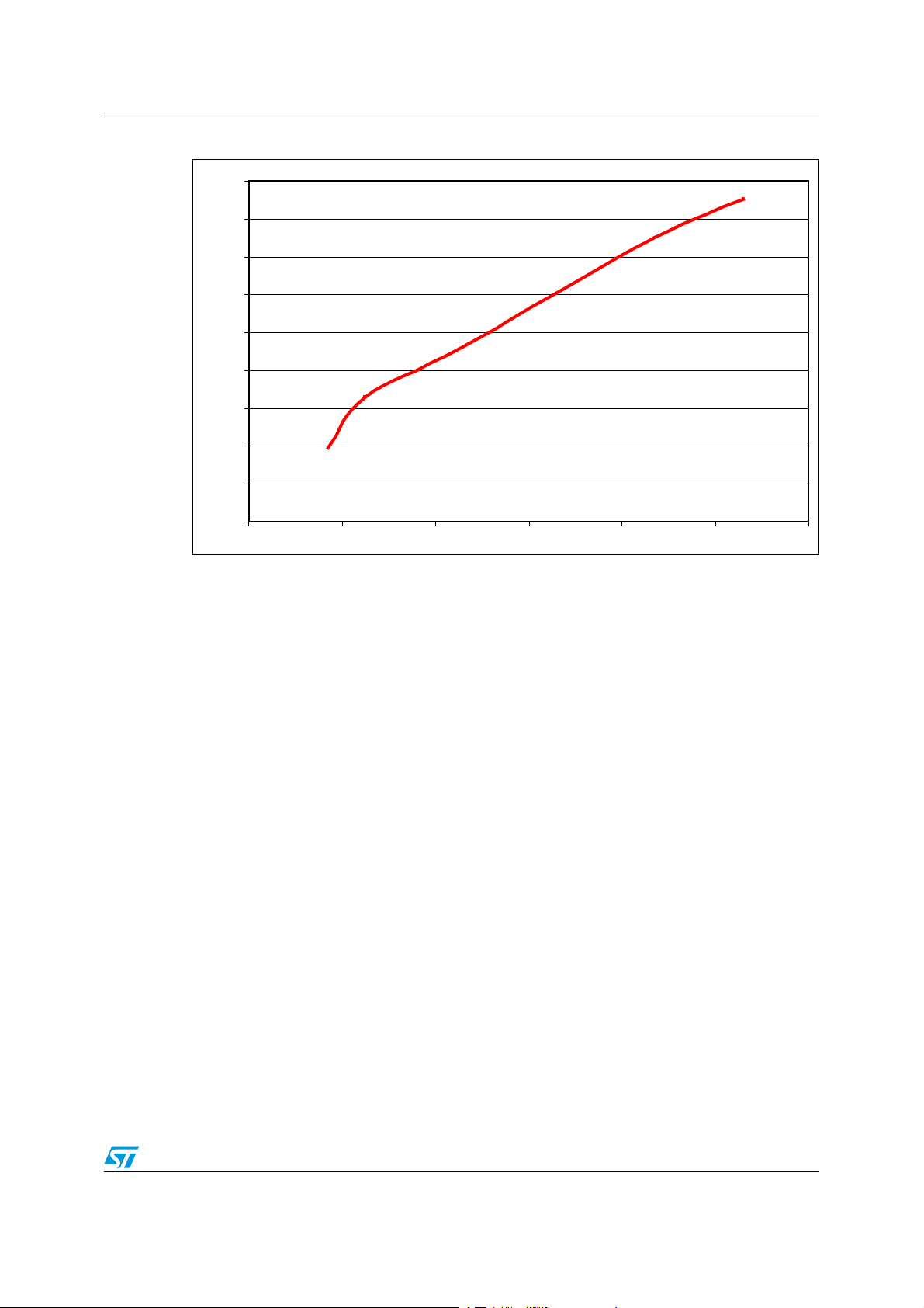
Figure 6. Efficiency vs. power output on BOOST stage @ R
Figure 7. Typical waveform during normal operation on BOOST stage @ P
Figure 8. Turn-on waveform on BOOST stage @ P
OUT
Figure 9. di/dt vs. gate resistance value @ total parasitic inductance of 110 nH on the power loop 12
Figure 10. I
Figure 11. Silicon vs. SiC diode comparison @ I
vs. di/dt @ P
peak
= 1900 W . . . . . . . . . . . . . . . . . . . . . . . . . . . . . . . . . . . . . . . . . . . . 13
OUT
= 5 A, di/dt = 840 A/µs. . . . . . . . . . . . . . . . . . . . . . 14
F
=8.2 Ω and di/dt = 1400 W . . . . . . . . . 9
g
= 1300 W . . . . . . . 10
OUT
= 1700 W, VIN = 200 V . . . . . . . . . . . . . . . . 11
Doc ID 17056 Rev 1 3/17
Page 4

Solar power systems and inverters AN3152
1 Solar power systems and inverters
There are a wide variety of topologies employed in the design of converters for solar power
systems, but they can be separated into two main classifications:
● Grid connected:
– These are usually isolated residential PV panels or collections of panels, called
“farms”, connected to a central power facility maintained by a private or public
company. Therefore, the energy produced from these photovoltaic modules during
the day can be used immediately on the main grid. These systems do not require
storage batteries or any backup system to store the energy, because the main grid
continues to supply energy at night or in the absence of sunlight.
● Standalone:
– These are used on systems typically far from a municipal or public power grid.
These systems use a battery, or bank of batteries, to store the energy produced
during the day by the panels, in order to provide a supply of energy at night or
when solar irradiation is low. Grid connected inverters are generally more complex
than the standalone because they must synchronize with the grid sinusoid and
supply the current within the same phase. However, the first stages of design are
quite the same on both types of inverters. Traditionally, solar systems used to
implement a single, shared inverter for all panels. This is called a “centralized”
system. The trend today is toward a “string inverter” system, in which each panel
is equipped with its own low power and high performance inverter. Each of the
inverters mentioned previously can be designed following two different
approaches with respect to frequency operation. If a low frequency approach is
adopted (typically 100 Hz), very slow devices can be used. However, in this case
very heavy transformers and bulk capacitors are necessary. Generally, newer
designs adopt high frequency operation in order to minimize inverter dimensions
and weight and to maximize performance. It is worth mentioning that in our
example we have performed the tests on a 3 kW grid-connected inverter, but the
same benefits can be obtained in each of the types of inverters previously
mentioned.
4/17 Doc ID 17056 Rev 1
Page 5
AN3152 Grid connected inverter
2 Grid connected inverter
A PV inverter must perform three main functions in order to feed energy from a PV array into
the utility grid:
1. Shape the current into a sinusoidal waveform
2. Invert the current into an AC current
3. Boost the PV array voltage if it is lower than the grid voltage
The way these functions are sequenced within an inverter design determines the choice of
semiconductor and passive components, and consequently their losses, sizes and prices. In
order to validate new technologies, a solar inverter prototype was developed and equipped
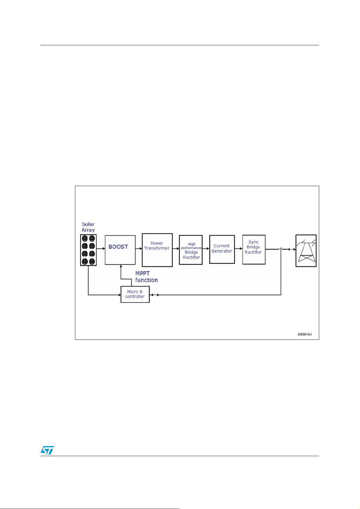
with ST MDmesh™ and SiC devices. The block diagram is shown in Figure 1, and block-byblock details are shown in Figures 2, 3, 4 and 5.
Note: The new approach and topologies of each stage allow the use of a 650 V power MDmesh™.
Figure 1. Block diagram
Doc ID 17056 Rev 1 5/17
Page 6
Grid connected inverter AN3152
Figure 2. BOOST stage
Figure 3. Power transformer and rectification stage
6/17 Doc ID 17056 Rev 1
Page 7

AN3152 Grid connected inverter
Figure 4. BUCK current generator stage
Figure 5. 100 Hz bridge sync rectifier stage
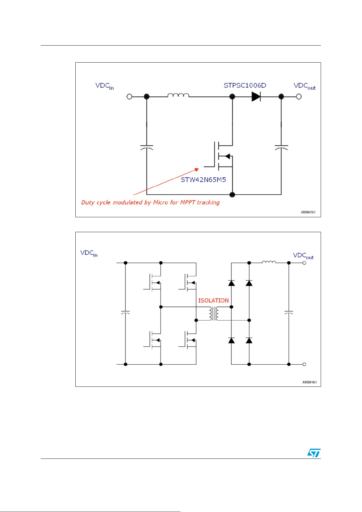
The first stage, called the “BOOST” stage, is common to most solar inverters and power
factor correction (PFC) converters. A converter used as a front-end between PV panels and
inverter, amplifies the panel voltage into a DC BUS from 400 V to 500 V for 3 kW output
power. The BUS voltage should be lower than 450 V in order to permit the use of 450 V
capacitors, typically less expensive than 500 V capacitors. In order to limit the peak value of
the current on both the power MOSFET and the diode, this BOOST stage operates in
Doc ID 17056 Rev 1 7/17
Page 8

Grid connected inverter AN3152
continuous current mode, so the power MOSFET is turned on during the recovery time of
the diode. The BOOST is driven from a microcontroller in order to implement the MPPT.
Some inverter modules adopt a push-pull topology instead of the boost topology, to elevate
the panel solar voltage and achieve galvanic insulation. In this case, more expensive
devices sized for two times the input voltage must be used. If the BUS voltage is 500 V, the
devices must be able to manage at least 1000 V, so 1200 V devices are needed. IGBTs are
commonly used for this voltage range, due to acceptable conduction loss levels.
Unfortunately, IGBTs are not fast devices and they must be used at relatively low
frequencies in order to minimize switching losses. The boost topology permits the use of
more efficient 600-650 V power MOSFET devices, and pushes up the switching frequency.
A higher frequency means smaller and cheaper inductor and bulk capacitors.
The second stage is a “power transformer” stage, as shown in Figure 3. This is used to
provide galvanic insulation between the panels and the grid. This block is not mandatory in
some countries but is generally used for safety reasons. Its frequency of operation is about
100 kHz in order to minimize transformer size. The power MOSFETs are connected in a
typical bridge configuration, and the devices work on a modified zero-voltage switching
(ZVS) modulation to minimize the switching losses. The bus voltage is 450 V (typ).
The “high performance bridge rectifier” stage is used to rectify the alternating voltage
coming from the “power transformer.” It is composed of four SiC diodes connected in a
Graetz bridge, as shown on the right side of Figure 3. These diodes are able to work at very
high di/dt, typically greater than 1000 A/µs. The operating frequency is the same as that of
the “power transformer” stage, about 100 kHz.
The “current generator” stage is used to provide and regulate the power generated from
solar panels onto the grid. It consists of a typical buck topology composed of an MDmesh™
V power MOSFET and a SiC diode, as shown in Figure 4. The operating frequency is about
100 kHz, and the drive signal is modulated in order to follow the 100 Hz of the grid.
The last stage is the “sync bridge rectifier.” This is a simple Graetz bridge used to rectify the
grid and allow the “current generator” to introduce power to the grid during the full sinusoid.
It is composed of four power MOSFETs specially driven and used as synchronous rectifiers
(see Figure 5). Please note that this stage can be realized with simple diodes, but for
efficiency issues we use a MOSFET as a synchronous rectifier, grid-commutated at twice
the grid frequency. Grid-commutated operation is possible because the input current to the
stage is modulated to the rectified sinusoidal by the “current generator” stage.
Thanks to this solution, a single switch current generator can be adopted using the
STW42N65M5 or STW77N65M5 650 V power MOSFETs. Currently, most solutions adopt a
half-bridge current generator topology instead of a single switch. These solutions are able to
follow the grid voltage on a full sinusoid, but 600-650 V power MOSFETs cannot be used
due to their low breakdown voltage. In fact, in this case the power MOSFETs must be able to
manage at least 750 V on the bus voltage (double the maximum peak-to-peak grid voltage ±
373 V). If a full-bridge inverter topology is used to design a current generator (to unfold the
power to grid, synchronized to the sine wave), PWM modulation must be used. Both fast
switches and diodes must be used in order to increase efficiency. IGBT devices with a
paralleled discrete fast diode are generally used, due to better performance with respect to
the power MOSFET solution. IGBTs are preferred based on the higher performance of the
discrete fast diodes with respect to a power MOSFET internal body diode. Due to the circuit
solutions adopted on this proposed new inverter design, 650 V MDmesh™ V MOSFETs can
be safely used (STW42N65M5 or STW77N65M5). Using MDmesh™ combined with 600 V
SiC diodes (STPSC1006) allows us to increase the frequency of operation and work at high
dI/dt, from 800 A/µs to 2 kA/µs, and more. The capability to operate at a high frequency
translates into being able to use the smallest (and magnetic) transformer, and even smaller
capacitors.
8/17 Doc ID 17056 Rev 1
Page 9

AN3152 Measurements on the BOOST stage
3 Measurements on the BOOST stage
Although MDmesh™ power MOSFETs and SiC diodes are used on every stage of the
inverter, the following results derive from the inverter front-end stage called the BOOST
stage. This stage is used as a case study to validate the performance of the fastest power
MOSFETs and diodes available on the market. The basic BOOST configuration is very
similar to other applications like a traditional single switch PFC, as shown in Figure 2, but in
this case, the input voltage is continuous rather than pulsed. Efficiency is measured in the
worst conditions, which means at the lowest input voltage, so that at full load the input
current is the highest possible. Note that higher-speed commutation leads to higher
efficiency, but at the same time spike voltage and current stimulus on the main switch are
higher also. Therefore finding a good trade-off is recommended. In any case, a 650 V
breakdown voltage keeps the MDmesh™ V within a safe working zone. An STW42N65M5
and an STPSC1006 are used for this stage. Figure 6 shows the efficiency versus output
power, at VDC
With 8.2 Ω, we achieved a di/dt of 1400 A/µs during turn-on, which provides good noise
immunity and low EMI irradiation.
= 200 V and gate resistance Rg= 8.2 Ω.
IN
Figure 6. Efficiency vs. power output on BOOST stage @ R
=8.2 Ω and
g
di/dt = 1400 W
Figure 7 shows the BOOST signals during normal operation at V
and P
200 V, V
= 1300 W. Figure 8 shows the detailed BOOST signals during turn-on at V
OUT
= 450 V, and P
OUT
= 1700 W. Please note the peak current on the trace in black
OUT
= 200 V, V
IN
OUT
= 450 V,
=
IN
Doc ID 17056 Rev 1 9/17
Page 10

Measurements on the BOOST stage AN3152
(about 22 A). This is due to the SiC capacitance discharge at high di/dt = 1400 A/µs. The
step on the drain voltage (trace in red) is due to parasitic inductance of the board. The violet
trace represents the energy losses during turn-on. Turn-off is performed with a signal diode
connected in parallel to the 8.2 Ω resistor, so for turn-off the equivalent R
GATE
is zero, in
order to obtain the fastest commutation speed. All measurements have bean performed on
a grid-connected 3 kW solar inverter prototype, totally equipped with both MDmesh™ and
SiC devices.
Figure 7. Typical waveform during normal operation on BOOST stage @
P
= 1300 W
OUT
10/17 Doc ID 17056 Rev 1
Page 11

AN3152 Measurements on the BOOST stage
Figure 8. Turn-on waveform on BOOST stage @ P
Table 1 summarizes the results of the measurements performed by varying the R
= 1700 W, VIN = 200 V
OUT
gate
g
resistor value. Please note that we use a gate resistor just for turn-on. For turn-off, a simple
diode is used, connected in parallel to the gate resistor. It should be highlighted that lower
R
values lead to improved efficiency over the entire power output scale. But at the same
g
time this means higher spike voltage and current during commutation. By using a lower gate
resistor you get better efficiency, but also higher peak recovery current and higher di/dt. This
could be a problem for EMI irradiation and reliability, so an 8.2 Ω and 1400 A di/dt should be
a good compromise.
Table 1. di/dt and I
Rg (Ω)I
vs. R
peak
di/dt (A/µs) I
ON
during turn-on @ P
gate
ONpeak
= 2000 W, VIN= 200 V
OUT
(A)
Efficiency @
P
OUT
= 2 kW (%)
3.9 2200 26.6 98.52
5.6 2000 24.7 98.40
8.2 1400 20.6 98.27
15 800 17.4 98.14
Although designers strive to keep all board parasitic influences to a minimum, they cannot
be eliminated completely due to the physical limitations related to component dimensions.
The copper tracks on the board must be as short as possible, but in any case must be long
Doc ID 17056 Rev 1 11/17
Page 12

Measurements on the BOOST stage AN3152
enough to connect every component. So, assuming that parasitic impedances are still
present, even if very small, they present problems in addition to an increase in operating
frequency. Parasitic effects lead to:
● losses during commutation
● spike voltage
● EMI irradiation
● reliability problems leading to failures in extreme cases
For this reason, designers tend to optimize the layout and limit the very fast commutations
by increasing the gate resistor. According to our tests, the I
tuning the R
gate resistance used to drive the power MOSFET during turn-on
g
di/dt can be controlled by fine
ON
(STW42N65M5). Figure 9 shows the di/dt vs. gate resistance value by using a board with
about 110 nH of total parasitic inductances (about 12 cm of total parasitic inductance on the
power ring loop). Figure 10 shows the peak current obtained by using a different gate
resistance value, with about 120 nH of total parasitic inductances. These graphs can be
useful to obtain a rough estimate of the gate resistor dimensions, with the di/dt function or
maximum peak current you wish to obtain, considering that di/dt commutation speed
depends on many parameters (such as power MOSFET + diode and the board). It is
recommended to test the results with the selected power MOSFET in every board, in order
to achieve the best performance. It should be noted that MDmesh™ power MOSFETs and
SiC diodes are able to work with very high di/dt, but in any case in a project it is preferable to
limit the commutation speed in order to keep EMI irradiations under control.
Figure 9. di/dt vs. gate resistance value @ total parasitic inductance of 110 nH on
the power loop
!-V
DIDT
!S
2
GATE/HM
12/17 Doc ID 17056 Rev 1
Page 13
AN3152 Measurements on the BOOST stage
Figure 10. I
DIDT
!S
vs. di/dt @ P
peak
OUT
= 1900 W
!-V
)
PEAK!
Doc ID 17056 Rev 1 13/17
Page 14

SiC technology vs. silicon AN3152
4 SiC technology vs. silicon
When using very fast power MOSFETs, the use of very fast diodes is also necessary in
order to prevent failures. Unfortunately, due to the relatively slow recovery of silicon diodes,
(even ultra-fast silicon diodes) they cannot be used in this project. In order to meet the new
requirements, ST has developed and introduced a new family of diodes using the new
silicon carbide technology. Silicon carbide diodes are virtually free of recovery current, even
if, due to the charge and discharge of the parasitic capacitance, a peak current is still
present during commutation. But this peak value is very low compared to a silicon diode
using the same forward and breakdown voltage. These devices are the best choice for a
high-end solar application where performance is the primary target. A comparison between
SiC and silicon diodes has been performed in a side-by-side test between a silicon ultra-fast
diode and a SiC with the same forward parameters, and using a di/dt = 800 A/µs.Table 2
provides the results of this comparison. Figure 11 shows the recovery at I
clearly shows that the silicon diode has a Q
the I
of the SiC diodes. This higher peak current triggers an immediate failure of the
RM
that is ten times higher and more than 3 times
rr
power MOSFET if it is used on the converter prototype. In other words, silicon diodes cannot
be used in this type of design where the di/dt is very high (from 800 A/µs to 2000 A/µs).
Table 2. Silicon vs. SiC diode comparison @ I
Parameter STPCS1006D STTH8L06D
= 5 A, di/dt = 840 A/µs
F
= 5 A. This
F
@5 A, TJ = 25 °C 1.12 1.2
V
F
V
@5 A, TJ = 150 °C 1.12 0.9
F
(nC) 26 293
Q
rr
(A) 3.7 9.9
I
RM
T
(ns) 13 44
rr
Figure 11. Silicon vs. SiC diode comparison @ IF = 5 A, di/dt = 840 A/µs
14/17 Doc ID 17056 Rev 1
Page 15

AN3152 Conclusion
5 Conclusion
The special requirements of the photovoltaic field provide an interesting application area for
ST’s new MDmesh™ V power MOSFETs and SiC diodes. These new technologies can
operate at high frequencies with very good efficiency, leading to a reduction in the size of
passive components, saving cost and board space. These innovative devices are tested in a
new PV inverter prototype. Thanks to performance of the 600-650 V power MOSFETs and
diodes used in the prototype, a new inverter topology is possible which permits galvanic
insulation with a good trade-off between cost, weight and size.
Doc ID 17056 Rev 1 15/17
Page 16

Revision history AN3152
6 Revision history
Table 3. Document revision history
Date Revision Changes
14-May-2010 1 Initial release.
16/17 Doc ID 17056 Rev 1
Page 17

AN3152
Please Read Carefully:
Information in this document is provided solely in connection with ST products. STMicroelectronics NV and its subsidiaries (“ST”) reserve the
right to make changes, corrections, modifications or improvements, to this document, and the products and services described herein at any
time, without notice.
All ST products are sold pursuant to ST’s terms and conditions of sale.
Purchasers are solely responsible for the choice, selection and use of the ST products and services described herein, and ST assumes no
liability whatsoever relating to the choice, selection or use of the ST products and services described herein.
No license, express or implied, by estoppel or otherwise, to any intellectual property rights is granted under this document. If any part of this
document refers to any third party products or services it shall not be deemed a license grant by ST for the use of such third party products
or services, or any intellectual property contained therein or considered as a warranty covering the use in any manner whatsoever of such
third party products or services or any intellectual property contained therein.
UNLESS OTHERWISE SET FORTH IN ST’S TERMS AND CONDITIONS OF SALE ST DISCLAIMS ANY EXPRESS OR IMPLIED
WARRANTY WITH RESPECT TO THE USE AND/OR SALE OF ST PRODUCTS INCLUDING WITHOUT LIMITATION IMPLIED
WARRANTIES OF MERCHANTABILITY, FITNESS FOR A PARTICULAR PURPOSE (AND THEIR EQUIVALENTS UNDER THE LAWS
OF ANY JURISDICTION), OR INFRINGEMENT OF ANY PATENT, COPYRIGHT OR OTHER INTELLECTUAL PROPERTY RIGHT.
UNLESS EXPRESSLY APPROVED IN WRITING BY AN AUTHORIZED ST REPRESENTATIVE, ST PRODUCTS ARE NOT
RECOMMENDED, AUTHORIZED OR WARRANTED FOR USE IN MILITARY, AIR CRAFT, SPACE, LIFE SAVING, OR LIFE SUSTAINING
APPLICATIONS, NOR IN PRODUCTS OR SYSTEMS WHERE FAILURE OR MALFUNCTION MAY RESULT IN PERSONAL INJURY,
DEATH, OR SEVERE PROPERTY OR ENVIRONMENTAL DAMAGE. ST PRODUCTS WHICH ARE NOT SPECIFIED AS "AUTOMOTIVE
GRADE" MAY ONLY BE USED IN AUTOMOTIVE APPLICATIONS AT USER’S OWN RISK.
Resale of ST products with provisions different from the statements and/or technical features set forth in this document shall immediately void
any warranty granted by ST for the ST product or service described herein and shall not create or extend in any manner whatsoever, any
liability of ST.
ST and the ST logo are trademarks or registered trademarks of ST in various countries.
Information in this document supersedes and replaces all information previously supplied.
The ST logo is a registered trademark of STMicroelectronics. All other names are the property of their respective owners.
© 2010 STMicroelectronics - All rights reserved
STMicroelectronics group of companies
Australia - Belgium - Brazil - Canada - China - Czech Republic - Finland - France - Germany - Hong Kong - India - Israel - Italy - Japan -
Malaysia - Malta - Morocco - Philippines - Singapore - Spain - Sweden - Switzerland - United Kingdom - United States of America
www.st.com
Doc ID 17056 Rev 1 17/17
 Loading...