

Page 1

AN3147
Application note
STM8L family power management
Introduction
This document is intended for application designers who require a hardware implementation
overview of low power modes in the STM8L product families. It shows how to use the
STM8L devices in these modes, explains differences between different modes and gives
several examples of how to select the best mode for your application needs.
This document is not intended to replace STM8L datasheets. All values given in this
document are for guidance only. Please, refer to the related datasheet to get guaranteed
values.
March 2010 Doc ID 17035 Rev 1 1/22
www.st.com
Page 2

Contents AN3147
Contents
1 Power consumption factors . . . . . . . . . . . . . . . . . . . . . . . . . . . . . . . . . . . 4
2 Power supply . . . . . . . . . . . . . . . . . . . . . . . . . . . . . . . . . . . . . . . . . . . . . . . 5
2.1 Internal supply structure for STM8L101xx devices . . . . . . . . . . . . . . . . . . 5
2.2 Internal supply structure for STM8L15x devices . . . . . . . . . . . . . . . . . . . . 6
2.2.1 Brownout detector (BOR) . . . . . . . . . . . . . . . . . . . . . . . . . . . . . . . . . . . . 6
3 Clock management . . . . . . . . . . . . . . . . . . . . . . . . . . . . . . . . . . . . . . . . . . 7
3.1 STM8L101xx clock system overview . . . . . . . . . . . . . . . . . . . . . . . . . . . . . 7
3.2 STM8L15x clock system overview . . . . . . . . . . . . . . . . . . . . . . . . . . . . . . . 7
3.3 Clock configuration and power management . . . . . . . . . . . . . . . . . . . . . . . 9
3.4 Clock selection vs. power consumption . . . . . . . . . . . . . . . . . . . . . . . . . . . 9
4 Run and low power modes . . . . . . . . . . . . . . . . . . . . . . . . . . . . . . . . . . . 10
4.1 Flash memory . . . . . . . . . . . . . . . . . . . . . . . . . . . . . . . . . . . . . . . . . . . . . 10
4.2 Overview of low power modes . . . . . . . . . . . . . . . . . . . . . . . . . . . . . . . . . 10
4.2.1 STM8L101xx low power modes . . . . . . . . . . . . . . . . . . . . . . . . . . . . . . . 11
4.2.2 STM8L15x low power modes . . . . . . . . . . . . . . . . . . . . . . . . . . . . . . . . . 11
4.3 Slowing down the clock frequency . . . . . . . . . . . . . . . . . . . . . . . . . . . . . . 12
4.4 Peripheral clock gating (PCG) . . . . . . . . . . . . . . . . . . . . . . . . . . . . . . . . . 12
4.5 Execution from RAM . . . . . . . . . . . . . . . . . . . . . . . . . . . . . . . . . . . . . . . . 12
4.6 Wait mode . . . . . . . . . . . . . . . . . . . . . . . . . . . . . . . . . . . . . . . . . . . . . . . . 13
4.6.1 Entering Wait mode . . . . . . . . . . . . . . . . . . . . . . . . . . . . . . . . . . . . . . . . 13
4.6.2 Exiting Wait for interrupt mode . . . . . . . . . . . . . . . . . . . . . . . . . . . . . . . . 13
4.6.3 Exiting Wait for event mode . . . . . . . . . . . . . . . . . . . . . . . . . . . . . . . . . . 13
4.7 Low power run mode . . . . . . . . . . . . . . . . . . . . . . . . . . . . . . . . . . . . . . . . 14
4.7.1 Entering Low power run mode . . . . . . . . . . . . . . . . . . . . . . . . . . . . . . . . 14
4.7.2 Exiting Low power run mode . . . . . . . . . . . . . . . . . . . . . . . . . . . . . . . . . 15
4.8 Low power wait mode . . . . . . . . . . . . . . . . . . . . . . . . . . . . . . . . . . . . . . . . 15
4.9 Halt mode . . . . . . . . . . . . . . . . . . . . . . . . . . . . . . . . . . . . . . . . . . . . . . . . . 15
4.9.1 Entering Halt mode . . . . . . . . . . . . . . . . . . . . . . . . . . . . . . . . . . . . . . . . 15
4.9.2 Exiting Halt mode . . . . . . . . . . . . . . . . . . . . . . . . . . . . . . . . . . . . . . . . . . 16
4.9.3 Active-halt mode . . . . . . . . . . . . . . . . . . . . . . . . . . . . . . . . . . . . . . . . . . 16
2/22 Doc ID 17035 Rev 1
Page 3

AN3147 Contents
4.10 Activation level control . . . . . . . . . . . . . . . . . . . . . . . . . . . . . . . . . . . . . . . 16
5 Power management tips . . . . . . . . . . . . . . . . . . . . . . . . . . . . . . . . . . . . . 17
5.1 Choosing the optimal low-power mode for your application . . . . . . . . . . . 17
5.2 GPIO initialization . . . . . . . . . . . . . . . . . . . . . . . . . . . . . . . . . . . . . . . . . . . 17
5.3 Dynamic control of pull-up resistor . . . . . . . . . . . . . . . . . . . . . . . . . . . . . . 17
5.4 Waiting loops / delays . . . . . . . . . . . . . . . . . . . . . . . . . . . . . . . . . . . . . . . . 18
5.5 Minimizing power consumption . . . . . . . . . . . . . . . . . . . . . . . . . . . . . . . . 19
6 Conclusion . . . . . . . . . . . . . . . . . . . . . . . . . . . . . . . . . . . . . . . . . . . . . . . . 20
7 Revision history . . . . . . . . . . . . . . . . . . . . . . . . . . . . . . . . . . . . . . . . . . . 21
Doc ID 17035 Rev 1 3/22
Page 4

Power consumption factors AN3147
IDD fI
DynamicRun
μA MHz⁄[]× I
Static
μA[]+=
1 Power consumption factors
The STM8L microcontrollers are digital logic devices using the complementary metal oxide
semiconductor (CMOS) technology. In this type of devices, power consumption is a sum of:
● Static power (mainly caused by transistor polarization and leakage)
● Dynamic power which depends on the supply voltage and the clock frequency. It is
calculated from the formula: Dynamic power = C x V²
– C is the CMOS load capacitance
– V is the supply voltage
– f is the clock frequency.
Static consumption is negligible compared to dynamic consumption when the clock is
running. In some low power modes, when no clock is running, static consumption is the
main consumption source.
● Total consumption is a sum of static and dynamic consumption
Consequently, power consumption depends on:
● The microcontroller unit (MCU) chip size: technology used, number of transistors,
analog features/peripherals embedded and used in the application.
● The MCU supply voltage: the amount of current used in CMOS logic is directly
proportional to the squared power supply voltage (V²). Thus, power consumption may
be reduced by lowering the MCU supply voltage. This is less critical for STM8L devices
than for other microcontrollers, as an internal voltage regulator is used but this could
have an influence for the remaining components on the board.
● The clock frequency: Power consumption may be reduced by decreasing the clock
frequency when fast processing is not required by the application.
● The number of active peripherals or used MCU features (CSS, BOR, PVD,...): the
greater the number of active peripherals or features, the greater the amount of
consumed power.
● The operating mode: Power consumption depends on which mode a particular
application is running (CPU on/off, oscillator on/off,...). For an application powered by a
battery, the consumption is very important. Usually, the average consumption should
be below a certain target value to ensure an optimum battery lifetime. This means that
an application can consume more for short periods of time and keep its average current
consumption below the target value.
x f, where:
4/10 Doc ID 17035 Rev 1
Page 5
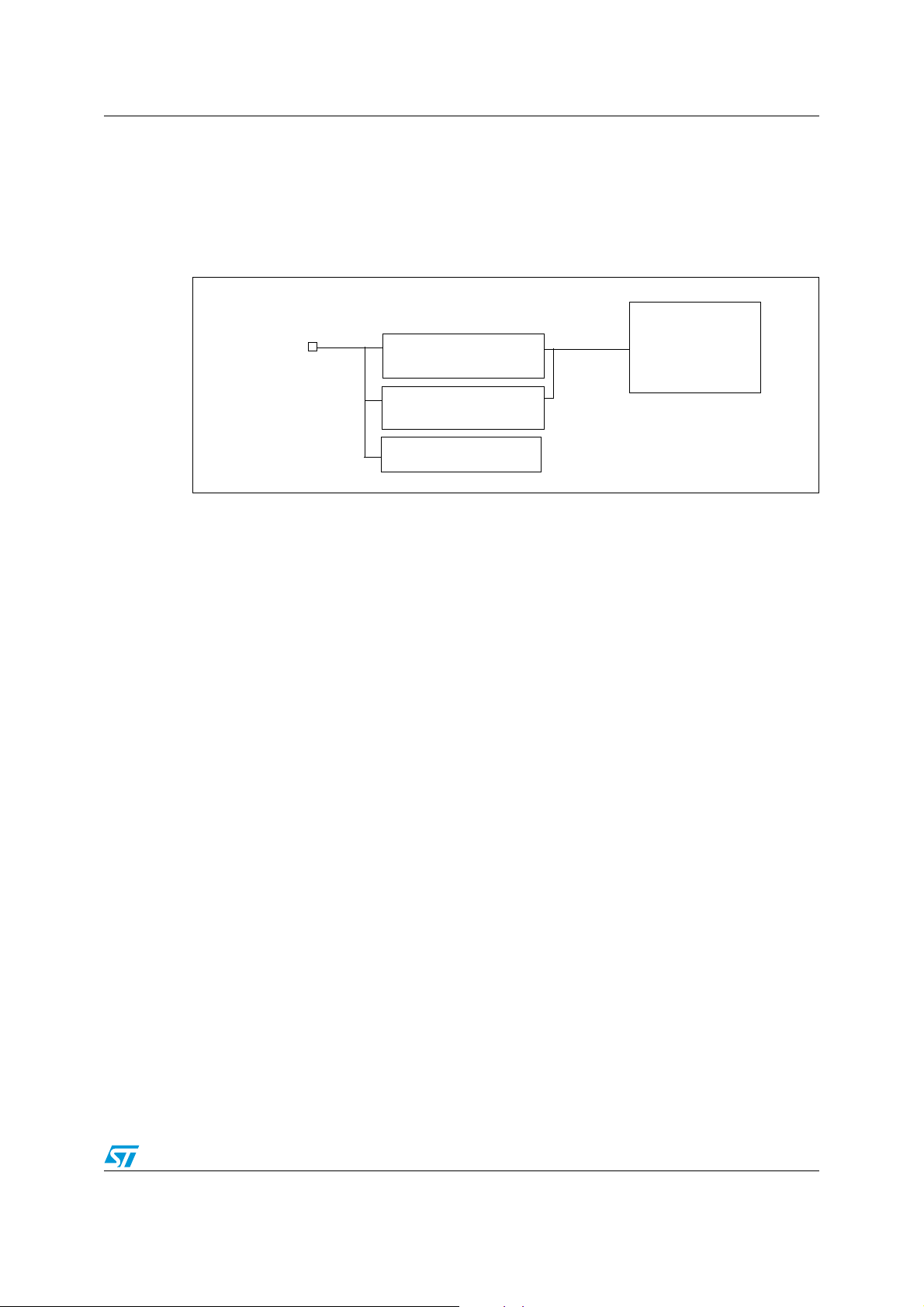
AN3147 Power supply
Low Power voltage regulator
V
DD
Main voltage regulator
I/Os
1.8 V domain
1)
1.65 V-3.6 V
RAM
Flash
STM8 MCU Core
CPU
(MVR)
(LPVR)
2 Power supply
The STM8L family embeds two regulators which provide a supply voltage (V
CORE
) for the
core and internal peripherals.
Figure 1. Power supply overview
1. If VDD is lower than 1.8 V, the 1.8 V domain is supplied by the voltage on the VDD input. For low power
modes where the LPVR is used, this domain is supplied by a 1.55 V voltage.
The main voltage regulator (MVR) provides a 1.8 V supply voltage. It has a high current
capability, as it can deliver up to 25 mA. However, the own consumption of this regulator is
higher than the own consumption of the LPVR. Consequently, the MVR is used during a
standard operation only.
The own consumption of the low power regulator (LPVR) is very low, as required for low
power modes. The LPVR can deliver up to 200 µA, providing 1.55 V to the digital part of the
MCU.
After reset, the MVR provides a supply voltage (V
) to the internal digital parts of the
CORE
microcontroller. Depending on the functional mode, the MVR can be switched off. In this
case, the LPVR continues to provide the V
CORE
voltage.
The power supply is monitored by the POR/PDR (power-on reset / power-down reset) and
and BOR (brown-out reset) system. This system ensures a proper startup and reset of the
MCU, while V
is rising above the POR threshold. It resets the MCU when VDD is falling
DD
below the PDR threshold.
Note: Analog peripherals require a power supply voltage above the PDR threshold (V
while V
= 1.5 V). In this case, it is recommended to use the BOR (Brownout reset) to
PDR
guarantee a proper functionality.
The BOR is available on STM8L15x devices only.
2.1 Internal supply structure for STM8L101xx devices
The STM8L101xx devices are able to operate from 1.65 V up to 3.6 V, connected to one pair
of supply pins.
There are no dedicated supply pins for the analog voltage domain. It is recommended to use
Doc ID 17035 Rev 1 5/10
> 1.8 V,
DD
Page 6

Power supply AN3147
a decoupling ceramic capacitor placed close to the supply pins.
● In Run and Wait modes, both MVR and LPVR provide the V
● In Halt / Active-halt modes, the LPVR is automatically used while the MVR is switched
CORE
.
off by the system in order to reduce current consumption.
2.2 Internal supply structure for STM8L15x devices
STM8L15x devices require a supply voltage of 1.8 V to 3.6 V. Once the supply voltage
reaches 1.8 V, the MCU can work down to 1.65 V with a limitation in the functionality of
analog peripherals.
The medium density STM8L15x devices have several supply pins, depending on the
package pincount. In addition to the main supply pair V
SS/VDD
could be present on the package.
It is recommended to use a decoupling ceramic capacitor, placed close to the supply pins.
● In Run and Wait modes, both MVR and LPVR provide the V
● In Low power run mode and Low power wait mode, the MVR has to be switched off.
Only the LPVR provides the V
● In Active-halt mode, during the Halt phase, either the MVR or the LPVR can provide the
V
. The user can select the regulator to be used.
CORE
● In Halt mode, the LPVR is automatically used, once MVR is switched off.
CORE
.
, another supply pin (V
.
CORE
DDA
)
2.2.1 Brownout detector (BOR)
The brownout detector is used to guarantee a proper functionality of all peripherals, mainly
analog ones. By default, this detector is enabled but the user can disable it through option
byte to decrease the MCU consumption by ~2.8 µA.
The BOR is mandatory to ensure a proper functionality of the product at power-down, to
cover a supply voltage area between V
Note: The BOR is available on STM8L15x devices only.
min. and V
DD
PDR
.
6/10 Doc ID 17035 Rev 1
Page 7

AN3147 Clock management
3 Clock management
3.1 STM8L101xx clock system overview
The 16 MHz high speed internal RC oscillator (HSI) is the only clock source that can be
used to drive the system clock.
The 38 kHz low speed internal RC oscillator (LSI) is only used to supply the auto-wakeup
unit (AWU) and watchdog.
Each peripheral clock can be switched on or off independently, in order to optimize power
consumption when the peripheral is not used. This is done by using the peripheral clock
gating (PCG) feature. See the “Clock control” section of the STM8L101xx reference manual
(RM0013) for more details.
3.2 STM8L15x clock system overview
Several different clock sources can be used to drive the system clock, depending on the
product and package you use:
● 1-16 MHz high speed external clock from the crystal oscillator (HSE crystal)
● Up to 16 MHz high speed external clock provided by the user (HSE bypass)
● 16 MHz high speed internal RC oscillator (HSI)
● 32.768 kHz low speed external crystal oscillator (LSE)
● 38 kHz low speed internal RC oscillator (LSI)
Each clock source can be switched on or off, depending on the actual needs of the
application. Each peripheral clock can be switched on or off independently, in order to
optimize power consumption when it is not used. This is done by using the peripheral clock
gating (PCG) feature. See the ‘Clock control’ section in the STM8L15x reference manual
(RM0031) for more details.
Several clock sources can be enabled in one time. The following table shows the main
features of each clock source. STM8L devices offer a complete range of clock sources to
meet customer application requirements in terms of cost, accuracy and consumption.
Doc ID 17035 Rev 1 7/10
Page 8

Clock management AN3147
Table 1. Clock sources
HSE oscillator external HSE HSI external LSE LSE crystal LSI
Cost Low to medium Low to high Free Low to medium
Accuracy ~ ppm / %
Consumption TBD High/medium
Start-up time 2 ms
Other
information
Crystal or
ceramic
resonator
depending on
external clock
depending on
external clock
Clock already
existing in the
system
~ %
100-200
µA
2 µs
depending on
external clock
depending on
external clock
Clock already
existing in the
system
The default clock source after reset is HSI / 8. The user can then switch the clock to different
frequencies and sources by using the following procedure:
● On the STM8L101xx devices:
– Choose the prescaler (/1, /2, /4 or /8) for an internal RC 16 MHz (HSI) clock
through the HSIDIV[1:0] bits in the CLK_CKDIVR register.
● On the STM8L15x devices
– Choose the prescaler (/1, /2 ... /128) for an internal RC 16 MHz (HSI) clock
through the CKM[2:0] bits in the CLK_CKDIVR register.
– Or change the system clock (to HSE, LSE or LSI ). Refer to the STM8L15x
reference manual (RM0031) for more details about the clock switching
mechanism.
Low to
medium
~ ppm ~ %
TBD
TBD TBD
Watch crystal
Free
100 - 400
nA
Before switching off a previous clock source when using automatic switching mode, the user
must ensure that the core is no longer running on the current clock. This means that the
previous clock must be turned off after the SWIF flag has been set. If the user tries to switch
off the clock and the SWIF flag has not been set by hardware, the current clock is not
switched off as the microcontroller is still running using this clock source.
Such clock switching can be combined with Wait mode (for example, if the HSE crystal is the
new clock) as clock switch execution interrupt can wake up the MCU from wait mode. This
enables the synchronization of the MCU wakeup with the new clock availability. The clock
switching feature can also be used at the beginning and the end of a regular or interrupt
routine to speed it up (for instance, if the clock master is LSI RC, but some parts of the code
have to be executed quickly with HSI RC).
8/10 Doc ID 17035 Rev 1
Page 9

AN3147 Clock management
IDD fI
DynamicRun
μAMHz⁄[]× I
Static
μA[]+=
IDD
STM8L101xx()
f 150 mA MHz⁄[]× 215 mA[]+=
3.3 Clock configuration and power management
In addition to the flexibility of the clock sources, different complementary clock
configurations and features are available to optimize the power consumption of the device:
● Each peripheral clock can be switched on/off through the CLK_PCKENRx registers.
● System clock divider from 1 to 8 (HSIDIV[1:0] bits in the CLK_CKDIVR register) is
available on STM8L101xx devices.
● System clock divider from 1 to 128 (CKM[2:0] bits in the CLK_CKDIVR register) is
available on STM8L15x devices.
Note: System clocks are used to supply both CPU and peripherals.
The STM8L is focused on low consumption. This is why all peripheral clocks are gated by
default. Before accessing any peripheral register, it is mandatory to enable the clock for the
given peripheral.
3.4 Clock selection vs. power consumption
The selected clock type and speed is one of the major factors influencing power
consumption of the MCU. In general, there are two parts in consumptions:
● A static part, depending on the number of enabled peripherals (mainly analog ones)
● A dynamic part, directly proportional to clock speed (increasing with higher clock
speed)
Note: The values given above are measured with all peripherals disabled.
Slowing down the clock decreases the immediate consumption but this is not the ideal
solution in many cases. By slowing down the clock, the CPU performance is also reduced.
Therefore, a longer time is required to perform an action or computation. If we consider the
average consumption, it might be better to use the highest available clock speed to perform
the required operation, and force the MCU to one of the low power modes (like Active-halt
mode) for the remaining time frame. This should be taken into account during the design of
application flowcharts.
Doc ID 17035 Rev 1 9/10
Page 10

Run and low power modes AN3147
4 Run and low power modes
By default, after a reset, the microcontroller is in Run mode. The default CPU clock is 2 MHz
(HSI / 8). Several low power modes are available to save power when the CPU is not used
for a standard operation (for instance: waiting for an external event). It is up to the user to
select the mode that gives the best compromise between low power consumption, short
startup time, good peripheral functionality, and availability of wakeup sources. Those power
modes are listed in Section 4.2.1 and Section 4.2.2.
Power consumption in Run and Wait modes can also be reduced by one of the following
means:
● Slowing down the system clocks
● Executing code from RAM
● Gating the clocks to the peripherals when they are not used.
4.1 Flash memory
On STM8L devices, the Flash memory supports a low power mode called I
mode, the Flash is switched off. It enters power-down mode (I
Active-halt, Low power wait or Low power run mode is entered.
By enabling the EEPM bit (available on STM8L15x and STM8L16x devices only) in the
FLASH_CR1 register, the Flash program memory automatically enters I
code is executed from RAM or when the device is in Wait mode. When the Flash program
memory is in I
mode, the recovery / wakeup time is longer (up to 2.8 µs) and depends
DDQ
on the supply voltage and temperature.
4.2 Overview of low power modes
The following table lists the STM8L low power modes and shows a basic behavior of STM8L
devices and the influence of different low power modes on CPU, peripherals and
consumption.
A detailed description of each mode is given in the following chapters.
In all low power modes, the general purpose I/Os continue to drive actively outputs (both
digital and analog - DAC).
The MCU can be woken up from these low power modes by specific interrupts, including
through comparators and incoming communications on SPI, I2C and/or USART. Refer to the
interrupt mapping table in the device datasheet.
. In this
) automatically when Halt,
DDQ
DDQ
mode when the
DDQ
10/10 Doc ID 17035 Rev 1
Page 11

AN3147 Run and low power modes
Table 2. Low power mode summary
Low power modes names
and consumptions
STM8L
typical
values
@ 3V / 25°C
Low power
modes
Low power
run
Low power
wait
Active-halt
w/ full RTC
Active-halt
w/ RTC
Entry
CPU Peripherals
Software
sequence
Software
sequence
+ WFE
ON
OFF
Can be
enabled
Can be
enabled
HALT OFF
Functions
High
speed
osc.
RTC
calendar
LSI
LSE
Flash RAM
OFF ON ON OFF ON 5.4 µA 6.8 µA
OFF ON ON OFF ON 3.3 µA 4.4 µA
ON ON OFF ON 1.0 µA
OFF ON OFF ON 0.8 µA
on LSI
Halt OFF OFF OFF ON 0.4 µA
1. Internal reference voltage and BOR off.
4.2.1 STM8L101xx low power modes
The STM8L101xx devices feature the following main low power modes:
● Wait mode: CPU stopped and peripherals kept running
● Active-halt mode: CPU stopped, AWU (auto-wakeup) and IWDG (independent
watchdog) kept running if enabled.
● Halt mode: CPU and peripheral clocks stopped
(1)
(1)
(1)
STM8L
typical
values
@ 3V / 85°C
1.4 µA
1.2 µA
1 µ A
4.2.2 STM8L15x low power modes
STM8L15x devices feature the following main low power modes:
● Wait mode: CPU clock stopped, peripherals kept running
● Low power run mode: executing code is done from RAM with a low speed oscillator
(LSI or LSE); selected peripherals remain active
● Low power wait mode: CPU clock stopped; selected peripherals remain active
● Active-halt mode: CPU clock stopped, AWU/RTC (auto wakeup/real-time clock) and
IWDG (independent watchdog) kept running if enabled
● Halt mode: everything is stopped.
Doc ID 17035 Rev 1 11/10
Page 12

Run and low power modes AN3147
4.3 Slowing down the clock frequency
In Run mode, choosing the clock frequency is very important to ensure the best compromise
between performance and consumption. The selection is done by programming the
prescaler registers. These prescalers can also be used to slow down peripherals before
entering low power modes.
Note: Keep in mind the recommendations given in Chapter 3.4 about performance and ratio
between Run mode and Halt mode operation.
4.4 Peripheral clock gating (PCG)
You can use peripheral clock gating (PCG) for additional power saving. This can be done at
any time by selectively enabling or disabling the clock connection to individual peripherals
through the CLK_PCKENRx registers. These settings are effective both in Run and Wait
modes.
Note: As all peripheral clocks are gated on STM8L devices after reset, it is mandatory to enable
the clock for a given peripheral before accessing any peripheral register.
4.5 Execution from RAM
The code can be executed from RAM in order to save power consumption. However, due to
the difference between size of data & instruction bus from Flash (32-bit) and RAM (8-bit),
the performance is degraded when the execution is done from RAM. This is important to
take into account the performance and the ratio between Run/Halt operations.
In this mode, the Flash memory can be forced to I
DDQ
mode.
The following figure shows the different bus widths for Flash and RAM memories.
Figure 2. STM8L architecture
)NSTRUCTION
-EMORY
$ATA%
2!-
0ERIPHERALS
BIT
BIT
BIT
-EMORY
#ONTROLLER
)"US
$"US
$EBUG
37)-
34-
#/2%
)NTERRUPTCONTROL
)4#
37)-PROTOCOL
)NTERRUPT
$-!
BIT
12/10 Doc ID 17035 Rev 1
AI
Page 13

AN3147 Run and low power modes
4.6 Wait mode
The STM8L devices support two different Wait modes: WFI (Wait for interrupt) and WFE
(Wait for event). Both modes are designed to reduce STM8L device power consumption by
switching off the core when it is not used. Wait mode is mainly used when the STM8L is
waiting for an external or internal event so that the program execution can continue.
The device can be switched to Wait mode instead of waiting for an Event in Run mode with:
While( ! Event );
This mode can be used with PCG and with a low speed clock source to further reduce the
power consumption of the device.
This mode offers the lowest wakeup time.
4.6.1 Entering Wait mode
Wait mode is entered by executing the WFI or WFE assembly instruction. This stops the
CPU, but other peripherals and the interrupt controller can continue to run. When entering
Wait mode, the global interrupts are automatically enabled.
● Before entering WFI mode, at least one interrupt must be enabled.
● Before entering WFE mode, at least one event source must be enabled.
4.6.2 Exiting Wait for interrupt mode
When an internal or external interrupt request occurs, the CPU wakes up from Wait mode
and resumes processing.
The following list gives examples of peripherals or features with interrupts having exit-fromwait capability:
● I2C
● USART
● SPI
● ADC
● Comparator
● AWU/RTC
● External interrupt
● Timers
● Clock controller (clock switch execution)
Refer to the STM8L reference manuals for more details. Refer to the STM8L datasheets for
the availability of the above peripherals and features on your devices.
4.6.3 Exiting Wait for event mode
When an internal or external event request occurs, the CPU wakes up from Wait mode and
resumes processing.
Doc ID 17035 Rev 1 13/10
Page 14

Run and low power modes AN3147
The following list gives examples of peripherals or features with events having exit-from-wait
capability:
● I2C
● USART
● SPI
● ADC
● Comparator
● External interrupt
● Timers
If an interrupt occurs during Wait for event mode, the related interrupt service routine is
executed. After this routine, the MCU goes back to Wait for event mode.
Refer to the STM8L reference manuals for more details. Refer to the STM8L datasheets for
the availability of the above peripherals and features on your devices.
4.7 Low power run mode
This mode is based on code execution from RAM, using a low speed clock source. The main
voltage regulator (MVR) is switched off and the low power voltage regulator (LPVR) is used
to supply the voltage to internal structures. The Flash memory is configured by software in
I
mode.
DDQ
The ADC is not supported in this mode, as its clock source must have a minimum frequency
of 1 MHz.
No interrupt is allowed in this mode as the interrupt vectors are located in the Flash (which is
switched off). Consequently, all interrupts must be masked.
While using this mode, you have to switch from high speed clock sources to low speed clock
sources.
Note: This mode is available only on the STM8L15x family.
4.7.1 Entering Low power run mode
This mode is entered by executing the following software sequence:
1. Switch off all unused peripherals, oscillators (except LSI or LSE) and analog blocks
2. Mask all interrupts
3. Jump to RAM
4. Switch system clock to LSI or LSE clock sources
5. Configure the Flash memory in I
register
6. Add a software delay loop to make sure the Flash/Data EEPROM are off
7. Configure the ultralow power mode for the regulator by setting the REGOFF bit in the
CLK_REGCSR register (do not confuse with the ULP bit in the PWR_CSR2 which
configures the behaviour of the internal reference voltage).
Steps 1 to 4 can be performed in any order.
mode by setting the EEPM bit in the FLASH_CR1
DDQ
14/10 Doc ID 17035 Rev 1
Page 15

AN3147 Run and low power modes
4.7.2 Exiting Low power run mode
The only way to exit this mode is to follow these steps:
1. Switch on the main regulator by resetting the REGOFF bit in the CLK_REGCSR
register. The REGREADY flag in the CLK_REGCSR register is set when the regulator
is ready.
2. Switch on the Flash/Data EEPROM by resetting the EEPM bit in the FLASH_CR1
register. The EEREADY flag in the CLK_REGCSR register is set when the Flash/Data
EEPROM is ready.
3. Switch the clock to HSI (or HSE).
4. Reset interrupt mask.
5. Switch on what is necessary and jump to Flash/Data EEPROM if needed.
4.8 Low power wait mode
This mode is entered by executing a WFE instruction, while the MCU is in Low power run
mode. It can be exited only by means of an external or internal event, in this case the MCU
returns to Low power run mode. WFI instruction cannot be used, because interrupts have to
be disabled in Low power run mode.
4.9 Halt mode
In this mode the system clock is stopped. This means that the CPU and all the peripherals
requiring clocks are disabled, except for the following cases:
● The HSI clock is not stopped if used by the SWIM
● The system clock source is not stopped if a Flash/Data EEPROM write operation is in
progress
● The LSI clock is not stopped if used by the SWIM, by the IWDG or if the “IWDG_HALT”
option bit is disabled.
In Halt mode, none of the peripherals is clocked and the digital part of the MCU consumes
almost no power.
4.9.1 Entering Halt mode
The MCU enters Halt mode when a HALT instruction is executed. Before executing a HALT
instruction, the application must clear any pending peripheral interrupt by clearing the
interrupt pending bit in the corresponding peripheral configuration register. Otherwise, the
HALT instruction is executed but the MCU wakes up immediately and the program execution
continues.
However, the Halt procedure can be delayed if one of the following flags is set:
● SWBSY flag in the CLK_SWCR register
● EEBUSY flag in the CLK_REGCSR register
● RTCSWBSY flag in the CLK_CRTCR register
● BEEPSWBSY flag in the CLK_CBEEPR register when the Beep is enabled in Active-
halt mode.
Doc ID 17035 Rev 1 15/10
Page 16

Run and low power modes AN3147
If the SAHALT bit is set in the CLK_ICKCR register, the main regulator (MVR) is switched off
without taking into account that some high speed clocks may be used by the system.
4.9.2 Exiting Halt mode
Wakeup from Halt mode is triggered by an external interrupt, sourced by a general purpose
I/O port configured as interrupt input or by an alternate function pin capable of triggering a
peripheral interrupt.
The system clock is then restarted at a frequency depending on the FHW bit in the
CLK_ICKCR register. If the FHW bit is set, HSI/8 is the system clock. Otherwise, the system
clock is the last selected clock source before the system enters Halt mode.
Note: When the STM8L101xx microcontroller is woken up from Halt mode, the same clock source
as that used before entering this mode is always selected.
In an interrupt-based application, where most of the processing is done through the interrupt
routines, the main program may be suspended by setting the activation level bit (AL) in the
CFG_GCR register. Refer to Section 4.10: Activation level control on page 16.
4.9.3 Active-halt mode
In Active-halt mode, the main oscillator, the CPU and almost all peripherals are stopped.
Only the LSI RC oscillator or the LSE crystal is running to drive the SWIM, beep, IWDG,
RTC and LCD, if enabled. The user can enter this mode by a HALT instruction, once some
of the peripherals above have been enabled.
4.10 Activation level control
The STM8L devices support an automatic activation level control feature. Consequently, the
user can configure the MCU so that it directly returns to a low power mode after it has been
woken up from such a mode through interrupts.
In an interrupt-based application, where most of the processing is done through the interrupt
routines, the main program may be suspended by setting the activation level bit (AL) in the
CFG_GCR register. Setting this bit causes the CPU to return to low power mode after
exiting an interrupt service routine without restoring the main execution context when the
IRET instruction is executed. This saves power by removing both the save/restore context
activity and the need for a main software loop execution for power management (in order to
return to low power mode).
To return to the main loop, the AL bit has to be cleared by software. This must be done at
least two clock cycles before the IRET instruction is executed.
16/10 Doc ID 17035 Rev 1
Page 17

AN3147 Power management tips
5 Power management tips
5.1 Choosing the optimal low-power mode for your application
Different low power modes can be selected depending on your application:
● Application powered by a battery where the MCU is in sleep mode most of the time:
– If the MCU is woken up due to external events, no time tracking is necessary and
power consumption has to be as low as possible. Then, Halt mode is advised to
extend battery life as much as possible.
– Active-halt mode with AWU/RTC clocked by the LSI is advised if the application
does not only depend on external events, but needs a non accurate periodic
wakeup. The LSE can be used to achieve a high timing precision.
● Application powered by a battery where the MCU is awake most of the time:
– Active-halt mode is advised if the MCU has to perform a few periodic actions
during which no peripheral has to remain enabled.
– Wait mode is advised if at least one peripheral has to remain enabled all the time
and an interrupt or event can wake up the MCU.
● Application supplied by mains but where consumption is critical:
– Run mode, with a clock prescaler adapted to the application requirement, is
advised if the MCU has to run all the time and low power modes cannot be used.
5.2 GPIO initialization
By default, the I/Os are configured as floating input.
It is important to change the configuration of all I/Os that are not connected to defined logic
signals so as to obtain one of the following configurations:
● input configuration with pull-up,
● or output configuration with a low (or high) logic level.
Otherwise, an increased consumption is generated by noise, as the internal Schmitt triggers
detecting this noise are toggling.
Floating I/Os could generate additional consumption in the range of a few 10 µA.
There are also parts with some unbonded I/Os (typically different packages of the same
product). Those I/Os are connected to a defined level by factory option configuration, unless
otherwised specified in the datasheet.
5.3 Dynamic control of pull-up resistor
Many applications have buttons which are used as a user interface. Those buttons are
connected to I/Os that are connected to V
up is used in order to have a defined logic level on these I/Os when the button is off.
Once the button is pressed, the I/O is grounded and it generates an additional current of ~
40 – 70 µA, drawn from the power supply. This current is negligible if the application is in
Run mode, but becomes very important for applications mainly running in low power modes.
once the buttons are pressed. An internal pull-
SS
Doc ID 17035 Rev 1 17/10
Page 18

Power management tips AN3147
For this type of applications, you can control the pull-up dynamically. Once a button is
pressed, the related service routine is executed. This routine disables the pull-up and the
interrupt, in order to save consumption while the button is pressed.
As the application has to check the button status regulary, this pull-up is enabled again
before this check. If the button is still pressed, this process is repeated. Once a button
release is detected, the pull-up remains on.
For this task, an I/O can be left floating for a short time frame, given by a check period,
generating an extra consumption in the range of ~10 µA. Therefore, the total current
consumption for a button press operation is lower than without this dynamic control.
5.4 Waiting loops / delays
In some cases, the application has to wait for an input from the user, slow peripheral (ADC),
or another external unit.
If there is no useful code to execute in the meantime, instead of using:
● a typical delay loop:
(delay = 0; delay < 0xFFFF; delay++)
_asm ("nop");
●
or a polling loop like:
ADC_CR1 I= ADC_START; // start conversion
while (!( ADC_SR & ADC_SR_EOC)); // wait for EOC bit set
it is recommended to use a more advanced solution, using a Wait for event mode:
1. Configure the ADC as a source of event
2. Enable an event by allowing the related interrupt:
WFE_CR2 I= ADC_COMP_EV; // enable ADC as a source of event
ADC_CR1 = ADC_EOCIE; // enable interrupt for end of conversion
An event is then generated after each conversion. The conversion starts as follows:
ADC_CR1 = ADC_START; // start conversion
_asm ("wfe");
The sequence described above uses WFE mode to wait for an end of conversion. This can
also be used for other sources like communication lines, etc. In case of external sources
(like interrupt from an I/O port), you can also consider using Halt mode.
18/10 Doc ID 17035 Rev 1
Page 19

AN3147 Power management tips
5.5 Minimizing power consumption
The following recommendations can help you choose the right configurations to minimize
the power consumption of your device in your application:
● Switch off all unused peripherals (peripherals are switched off by default) and use the
PCG feature (through the CLK_PCKENRx registers) to disable the clock provided to
the unused peripherals (these clocks are disabled by default).
● All unused pins must be connected to a defined logic level. One of the option is to
configure them as output low level. Make sure there are no unused I/O pins configured
as a floating input. This needlessly leads to a high consumption.
● Use Wait mode if you need external wakeup capability in low power mode and if some
peripherals have to remain active.
● Use the appropriate V
consumed power.
Thanks to the internal regulator, which supplies internal structures of the MCU, there is
no major difference in the MCU consumption but the difference could be visible on an
application level, e.g. due to the current flowing through pull-up resistors out of the
MCU.
● Use Low power run mode and Halt modes as much as possible. To achieve this, you
need to shorten the time spent in the Run mode, for example by using the highest clock
speed in Run mode.
● When a low power mode cannot be used, use the minimum possible frequency for your
application. You can select the frequency value that meets your requirements.
● Use the dynamic control of pull-up configuration if possible. See Section 5.2: GPIO
initialization on page 17 for a the detailed description.
value for your application. The higher the VDD value, the more
DD
Doc ID 17035 Rev 1 19/10
Page 20

Conclusion AN3147
6 Conclusion
The STM8L family offers many possibilities for development of low consumption
applications. The user can take advantage of various low power modes like Wait, Low power
Run/Wait, or Halt and Active-halt modes. He can also reduce consumption by switching off
peripherals when they are not used. Another important point is the optimization of the ratio
between Run and Halt modes due to the good performance of the CPU itself.
The main important principles are described in this application note, including a few hints on
how and when to use it. Much more examples exist, depending on your exact needs. You
can find them on www.st.com.
20/10 Doc ID 17035 Rev 1
Page 21
AN3147 Revision history
7 Revision history
Table 3. Document revision history
Date Revision Changes
31-Mar-2010 1 Initial release
Doc ID 17035 Rev 1 21/10
Page 22

AN3147
Please Read Carefully:
Information in this document is provided solely in connection with ST products. STMicroelectronics NV and its subsidiaries (“ST”) reserve the
right to make changes, corrections, modifications or improvements, to this document, and the products and services described herein at any
time, without notice.
All ST products are sold pursuant to ST’s terms and conditions of sale.
Purchasers are solely responsible for the choice, selection and use of the ST products and services described herein, and ST assumes no
liability whatsoever relating to the choice, selection or use of the ST products and services described herein.
No license, express or implied, by estoppel or otherwise, to any intellectual property rights is granted under this document. If any part of this
document refers to any third party products or services it shall not be deemed a license grant by ST for the use of such third party products
or services, or any intellectual property contained therein or considered as a warranty covering the use in any manner whatsoever of such
third party products or services or any intellectual property contained therein.
UNLESS OTHERWISE SET FORTH IN ST’S TERMS AND CONDITIONS OF SALE ST DISCLAIMS ANY EXPRESS OR IMPLIED
WARRANTY WITH RESPECT TO THE USE AND/OR SALE OF ST PRODUCTS INCLUDING WITHOUT LIMITATION IMPLIED
WARRANTIES OF MERCHANTABILITY, FITNESS FOR A PARTICULAR PURPOSE (AND THEIR EQUIVALENTS UNDER THE LAWS
OF ANY JURISDICTION), OR INFRINGEMENT OF ANY PATENT, COPYRIGHT OR OTHER INTELLECTUAL PROPERTY RIGHT.
UNLESS EXPRESSLY APPROVED IN WRITING BY AN AUTHORIZED ST REPRESENTATIVE, ST PRODUCTS ARE NOT
RECOMMENDED, AUTHORIZED OR WARRANTED FOR USE IN MILITARY, AIR CRAFT, SPACE, LIFE SAVING, OR LIFE SUSTAINING
APPLICATIONS, NOR IN PRODUCTS OR SYSTEMS WHERE FAILURE OR MALFUNCTION MAY RESULT IN PERSONAL INJURY,
DEATH, OR SEVERE PROPERTY OR ENVIRONMENTAL DAMAGE. ST PRODUCTS WHICH ARE NOT SPECIFIED AS "AUTOMOTIVE
GRADE" MAY ONLY BE USED IN AUTOMOTIVE APPLICATIONS AT USER’S OWN RISK.
Resale of ST products with provisions different from the statements and/or technical features set forth in this document shall immediately void
any warranty granted by ST for the ST product or service described herein and shall not create or extend in any manner whatsoever, any
liability of ST.
ST and the ST logo are trademarks or registered trademarks of ST in various countries.
Information in this document supersedes and replaces all information previously supplied.
The ST logo is a registered trademark of STMicroelectronics. All other names are the property of their respective owners.
© 2010 STMicroelectronics - All rights reserved
STMicroelectronics group of companies
Australia - Belgium - Brazil - Canada - China - Czech Republic - Finland - France - Germany - Hong Kong - India - Israel - Italy - Japan -
Malaysia - Malta - Morocco - Philippines - Singapore - Spain - Sweden - Switzerland - United Kingdom - United States of America
www.st.com
22/22 Doc ID 17035 Rev 1
 Loading...