

Page 1
AN3139
Application note
Migration and compatibility guidelines
for STM8L microcontroller applications
Introduction
For designers of STM8L microcontroller applications, it is important to be able to replace
easily one microcontroller type by another one in the same product family. Migrating an
application to a different microcontroller is often needed when product requirements grow,
putting extra demands on the memory size and on the number of I/Os.
However, to achieve cost reduction objectives, the user may need to switch to smaller
components and to shrink the PCB area. This application note aims at analyzing the steps
required to migrate from an existing STM8L-based design to any one of the other
microcontroller types in the fast-growing STM8L family.
This application note groups all the most important information and provides a list of the
fundamental aspects.
The information included in this document can also be extremely useful in a first STM8
design. Studying the issues in this phase can allow the user to adapt from the beginning his
design to any future requirement.
To benefit fully from the information in this application note, the user should be familiar with
the STM8L microcontroller family. The STM8L family reference manuals (RM0013 and
RM0031), the STM8L datasheets, and the STM8L Flash program memory / data EEPROM
programming manual (PM0054) are available from www.st.com.
This application note is divided into four main sections:
■ Section 1: STM8L family compatibility: This section presents a first-level view of the
different aspects of the STM8L family architecture that must be taken into account for a
new design or migration. The microcontroller blocks and peripherals are grouped and
identified either as “compatible” or “compatible with minor limitations”.
■ Section 2: Planning for migration: This section gives an overview of common migration
cases. It provides a checklist of items which are potentially impacted by each case to allow
the user to quickly analyze which subjects have to be anticipated.
■ Section 3: Block-by-block compatibility: This section focuses on the migration
between different packages and details the pin-to-pin compatibility between all STM8L
sub-families.
■ Section 4: Peripheral pinout through all STM8L sub-families. This section shows the
differences in the pinout for each peripheral.
September 2011 Doc ID 16993 Rev 3 1/63
www.st.com
Page 2

Contents AN3139
Contents
1 STM8L family compatibility . . . . . . . . . . . . . . . . . . . . . . . . . . . . . . . . . . . 6
1.1 Family concept . . . . . . . . . . . . . . . . . . . . . . . . . . . . . . . . . . . . . . . . . . . . . . 6
1.2 Fully compatible blocks . . . . . . . . . . . . . . . . . . . . . . . . . . . . . . . . . . . . . . . 9
1.3 Blocks that are compatible with minor exceptions . . . . . . . . . . . . . . . . . . . 9
1.4 Blocks that are compatible with significant exceptions . . . . . . . . . . . . . . . 10
1.5 Firmware library . . . . . . . . . . . . . . . . . . . . . . . . . . . . . . . . . . . . . . . . . . . . 11
2 Planning for migration . . . . . . . . . . . . . . . . . . . . . . . . . . . . . . . . . . . . . . 26
2.1 Hardware migration . . . . . . . . . . . . . . . . . . . . . . . . . . . . . . . . . . . . . . . . . 26
2.2 Application resources and firmware migration . . . . . . . . . . . . . . . . . . . . . 26
3 Block-by-block compatibility analysis . . . . . . . . . . . . . . . . . . . . . . . . . 29
3.1 Package pinout . . . . . . . . . . . . . . . . . . . . . . . . . . . . . . . . . . . . . . . . . . . . . 29
3.1.1 Digital power supply . . . . . . . . . . . . . . . . . . . . . . . . . . . . . . . . . . . . . . . . 29
3.1.2 ADC power supply and voltage reference . . . . . . . . . . . . . . . . . . . . . . . 30
3.1.3 Alternate functions . . . . . . . . . . . . . . . . . . . . . . . . . . . . . . . . . . . . . . . . . 30
3.2 GPIO and peripheral registers . . . . . . . . . . . . . . . . . . . . . . . . . . . . . . . . . 30
3.2.1 Mapping overview . . . . . . . . . . . . . . . . . . . . . . . . . . . . . . . . . . . . . . . . . 30
3.2.2 GPIO . . . . . . . . . . . . . . . . . . . . . . . . . . . . . . . . . . . . . . . . . . . . . . . . . . . 34
3.3 Advanced, general purpose and basic timers . . . . . . . . . . . . . . . . . . . . . 36
3.4 ADC modes . . . . . . . . . . . . . . . . . . . . . . . . . . . . . . . . . . . . . . . . . . . . . . . 38
3.5 DAC peripheral . . . . . . . . . . . . . . . . . . . . . . . . . . . . . . . . . . . . . . . . . . . . . 40
3.6 COMP peripherals . . . . . . . . . . . . . . . . . . . . . . . . . . . . . . . . . . . . . . . . . . 41
3.7 LCD peripheral . . . . . . . . . . . . . . . . . . . . . . . . . . . . . . . . . . . . . . . . . . . . . 43
3.8 Communication peripherals . . . . . . . . . . . . . . . . . . . . . . . . . . . . . . . . . . . 46
3.8.1 SPI . . . . . . . . . . . . . . . . . . . . . . . . . . . . . . . . . . . . . . . . . . . . . . . . . . . . . 46
3.8.2 I2C . . . . . . . . . . . . . . . . . . . . . . . . . . . . . . . . . . . . . . . . . . . . . . . . . . . . . 46
3.8.3 USART . . . . . . . . . . . . . . . . . . . . . . . . . . . . . . . . . . . . . . . . . . . . . . . . . . 46
3.9 Clock controller . . . . . . . . . . . . . . . . . . . . . . . . . . . . . . . . . . . . . . . . . . . . . 47
3.9.1 LSI clock frequency . . . . . . . . . . . . . . . . . . . . . . . . . . . . . . . . . . . . . . . . 48
3.9.2 HSI clock frequency . . . . . . . . . . . . . . . . . . . . . . . . . . . . . . . . . . . . . . . . 48
3.10 BEEP . . . . . . . . . . . . . . . . . . . . . . . . . . . . . . . . . . . . . . . . . . . . . . . . . . . . 48
2/63 Doc ID 16993 Rev 3
Page 3

AN3139 Contents
3.11 RTC . . . . . . . . . . . . . . . . . . . . . . . . . . . . . . . . . . . . . . . . . . . . . . . . . . . . . 48
3.12 DMA . . . . . . . . . . . . . . . . . . . . . . . . . . . . . . . . . . . . . . . . . . . . . . . . . . . . . 49
3.13 Memory . . . . . . . . . . . . . . . . . . . . . . . . . . . . . . . . . . . . . . . . . . . . . . . . . . 51
3.13.1 Flash program memory . . . . . . . . . . . . . . . . . . . . . . . . . . . . . . . . . . . . . 51
3.13.2 Data EEPROM memory . . . . . . . . . . . . . . . . . . . . . . . . . . . . . . . . . . . . . 52
3.13.3 Boot ROM memory . . . . . . . . . . . . . . . . . . . . . . . . . . . . . . . . . . . . . . . . 52
3.13.4 RAM memory . . . . . . . . . . . . . . . . . . . . . . . . . . . . . . . . . . . . . . . . . . . . . 52
3.13.5 Stack . . . . . . . . . . . . . . . . . . . . . . . . . . . . . . . . . . . . . . . . . . . . . . . . . . . 53
3.14 Interrupt mapping . . . . . . . . . . . . . . . . . . . . . . . . . . . . . . . . . . . . . . . . . . . 53
3.15 Option bytes . . . . . . . . . . . . . . . . . . . . . . . . . . . . . . . . . . . . . . . . . . . . . . . 56
4 Peripheral pinout through all STM8L sub-families . . . . . . . . . . . . . . . . 58
4.1 Timer pinout . . . . . . . . . . . . . . . . . . . . . . . . . . . . . . . . . . . . . . . . . . . . . . . 58
4.2 SPI . . . . . . . . . . . . . . . . . . . . . . . . . . . . . . . . . . . . . . . . . . . . . . . . . . . . . . 59
4.3 I2C . . . . . . . . . . . . . . . . . . . . . . . . . . . . . . . . . . . . . . . . . . . . . . . . . . . . . . 60
4.4 USART . . . . . . . . . . . . . . . . . . . . . . . . . . . . . . . . . . . . . . . . . . . . . . . . . . . 60
4.5 DAC . . . . . . . . . . . . . . . . . . . . . . . . . . . . . . . . . . . . . . . . . . . . . . . . . . . . . 61
5 Revision history . . . . . . . . . . . . . . . . . . . . . . . . . . . . . . . . . . . . . . . . . . . 62
Doc ID 16993 Rev 3 3/63
Page 4

List of tables AN3139
List of tables
Table 1. Overview of STM8L family peripherals . . . . . . . . . . . . . . . . . . . . . . . . . . . . . . . . . . . . . . . . . 7
Table 2. STM8L firmware library compatibility . . . . . . . . . . . . . . . . . . . . . . . . . . . . . . . . . . . . . . . . . 15
Table 3. STM8L family migration products . . . . . . . . . . . . . . . . . . . . . . . . . . . . . . . . . . . . . . . . . . . . 28
Table 4. Overview of STM8L family packages . . . . . . . . . . . . . . . . . . . . . . . . . . . . . . . . . . . . . . . . . 29
Table 5. Overview of STM8L family memory addresses . . . . . . . . . . . . . . . . . . . . . . . . . . . . . . . . . 31
Table 6. Overview of STM8L family peripheral addresses . . . . . . . . . . . . . . . . . . . . . . . . . . . . . . . . 32
Table 7. STM8L family GPIOs overview . . . . . . . . . . . . . . . . . . . . . . . . . . . . . . . . . . . . . . . . . . . . . . 35
Table 8. Features of advanced, general purpose and basic timers . . . . . . . . . . . . . . . . . . . . . . . . . 36
Table 9. STM8L family timers overview . . . . . . . . . . . . . . . . . . . . . . . . . . . . . . . . . . . . . . . . . . . . . . 37
Table 10. Overview of STM8L family timer internal trigger. . . . . . . . . . . . . . . . . . . . . . . . . . . . . . . . . 37
Table 11. Overview of STM8L family ADC channels . . . . . . . . . . . . . . . . . . . . . . . . . . . . . . . . . . . . . 38
Table 12. TIMx internal triggers . . . . . . . . . . . . . . . . . . . . . . . . . . . . . . . . . . . . . . . . . . . . . . . . . . . . . 40
Table 13. Overview of STM8L family DACTIMx triggers . . . . . . . . . . . . . . . . . . . . . . . . . . . . . . . . . . 40
Table 14. Overview of comparator inputs . . . . . . . . . . . . . . . . . . . . . . . . . . . . . . . . . . . . . . . . . . . . . . 41
Table 15. Overview of STM8L family LCD pins . . . . . . . . . . . . . . . . . . . . . . . . . . . . . . . . . . . . . . . . . 43
Table 16. USART special features . . . . . . . . . . . . . . . . . . . . . . . . . . . . . . . . . . . . . . . . . . . . . . . . . . . 47
Table 17. Overview of the clocks in the STM8L family . . . . . . . . . . . . . . . . . . . . . . . . . . . . . . . . . . . . 48
Table 18. Overview of STM8L family DMA requests . . . . . . . . . . . . . . . . . . . . . . . . . . . . . . . . . . . . . 49
Table 19. Overview of the STM8L family Flash interface . . . . . . . . . . . . . . . . . . . . . . . . . . . . . . . . . . 51
Table 20. STM8L interrupt vector differences. . . . . . . . . . . . . . . . . . . . . . . . . . . . . . . . . . . . . . . . . . . 53
Table 21. Overview of the STM8L family interrupt vectors . . . . . . . . . . . . . . . . . . . . . . . . . . . . . . . . . 54
Table 22. Option byte addresses . . . . . . . . . . . . . . . . . . . . . . . . . . . . . . . . . . . . . . . . . . . . . . . . . . . . 56
Table 23. Timer pinout . . . . . . . . . . . . . . . . . . . . . . . . . . . . . . . . . . . . . . . . . . . . . . . . . . . . . . . . . . . . 58
Table 24. SPI pinout . . . . . . . . . . . . . . . . . . . . . . . . . . . . . . . . . . . . . . . . . . . . . . . . . . . . . . . . . . . . . . 59
Table 25. I2C pinout . . . . . . . . . . . . . . . . . . . . . . . . . . . . . . . . . . . . . . . . . . . . . . . . . . . . . . . . . . . . . . 60
Table 26. USART pinout . . . . . . . . . . . . . . . . . . . . . . . . . . . . . . . . . . . . . . . . . . . . . . . . . . . . . . . . . . . 60
Table 27. DAC pinout . . . . . . . . . . . . . . . . . . . . . . . . . . . . . . . . . . . . . . . . . . . . . . . . . . . . . . . . . . . . . 61
Table 28. Document revision history . . . . . . . . . . . . . . . . . . . . . . . . . . . . . . . . . . . . . . . . . . . . . . . . . 62
4/63 Doc ID 16993 Rev 3
Page 5

AN3139 List of figures
List of figures
Figure 1. STM8L family block diagram . . . . . . . . . . . . . . . . . . . . . . . . . . . . . . . . . . . . . . . . . . . . . . . 11
Figure 2. STM8L10x code example . . . . . . . . . . . . . . . . . . . . . . . . . . . . . . . . . . . . . . . . . . . . . . . . . . 13
Figure 3. STM8L15x code example . . . . . . . . . . . . . . . . . . . . . . . . . . . . . . . . . . . . . . . . . . . . . . . . . . 13
Doc ID 16993 Rev 3 5/63
Page 6

STM8L family compatibility AN3139
1 STM8L family compatibility
1.1 Family concept
The STM8L family is one of a growing number of different STM8 microcontroller families.
All these STM8 microcontroller families are based on a common robust and low-cost 8-bit
high performance core with a rich set of enhanced peripherals. This ensures a high level of
compatibility within the STM8L ‘world’, especially in terms of software development,
compilers, debugging environment, programming tools and driver libraries.
The STM8L product family offers a wide choice of memory sizes and package types to fit
different application requirements as closely as possible. Consequently, when there are new
requirements on the application side, it can make sense to switch to another STM8L type
with different memory capacity or package size.
The STM8L family includes a product line divided into two main sub-families:
● STM8L15x/STM8L16x sub-family of microcontrollers with different memory densities,
packages and peripherals.
– The low density STM8L15x devices are the STM8L151C2/K2/G2/F2,
STM8L151C3/K3/G3/F3 microcontrollers with a 4-Kbyte or 8-Kbyte Flash memory
density.
– The medium density STM8L15x devices are the STM8L151C4/K4/G4,
STM8L151C6/K6/G6, STM8L152C4/K4/G4 and STM8L152C6/K6/G6
microcontrollers with a 16-Kbyte or 32-Kbyte Flash memory density.
– The medium+ density STM8L15x devices are the STM8L151R6 and
STM8L152R6 microcontrollers with a 32-Kbyte Flash memory density. They offer
a wider range of peripherals than the medium density devices.
– The high density STM8L15x devices are the STM8L151x8 and STM8L152x8
microcontrollers with a Flash memory density equal to 64 Kbytes. They offer the
same peripheral set as medium+ density devices.
– The high density STM8L162x devices are the STM8L162x8 microcontrollers
where the Flash memory density is equal to 64 Kbytes. They offer the same
peripheral set as high density STM8L152 devices plus the AES hardware
accelerator.
● STM8L10x low density sub-family where the Flash memory density ranges between 4
and 8 Kbytes. The STM8L10x MCUs are ideal for cost-sensitive applications with low
code density.
Both sub-families provide a complete set of essential peripherals. STM8L10x devices target
applications requiring reduced cost, lower memory capacity, fewer GPIOs and less
advanced features.
The wide range of available pin-counts and package sizes is discussed in Chapter 3.1:
Package pinout.
6/63 Doc ID 16993 Rev 3
Page 7
AN3139 STM8L family compatibility
All STM8L family microcontrollers use the same application development tools:
● Embedded single wire interface module (SWIM)
● Software integrated development environment (IDE) tools including assembler,
simulator, debugger, programmer:
– ST Visual Develop (ST)
– Ride (Raisonance)
–IAR
● In-circuit debugging and programming tools
– STIce from ST (full hardware emulator)
– ST-Link from ST
– RLink from Raisonance (low cost debug/programming tool)
● Starter kits and evaluation boards
● C compiler and assembler tool chains (Cosmic, Raisonance, IAR)
● Firmware libraries (peripheral control examples, MISRA or class B compliance, touch
sensing)
● Application notes
By using a common development environment, you significantly reduce code maintenance
effort and shorten the time-to-market, especially in cases when an application has to be
migrated from one STM8 microcontroller to another.
By using the drivers provided in the STM8L firmware library to interface with the hardware, it
becomes reasonably straightforward to move the application firmware from one STM8L
product to another. The principle job is analyzing the details on the hardware side, taking
care of the placement and availability of the peripheral I/O functions in the pinout. More
details can be obtained in the STM8L datasheet and further in this document in Section 3.1:
Package pinout.
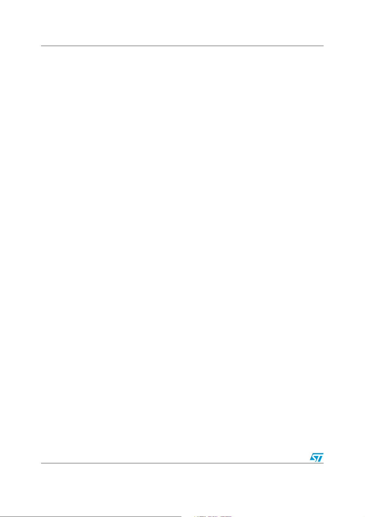
Figure 1: STM8L family block diagram gives an overview of the STM8L blocks and their
compatibility level, as discussed in the next sections.
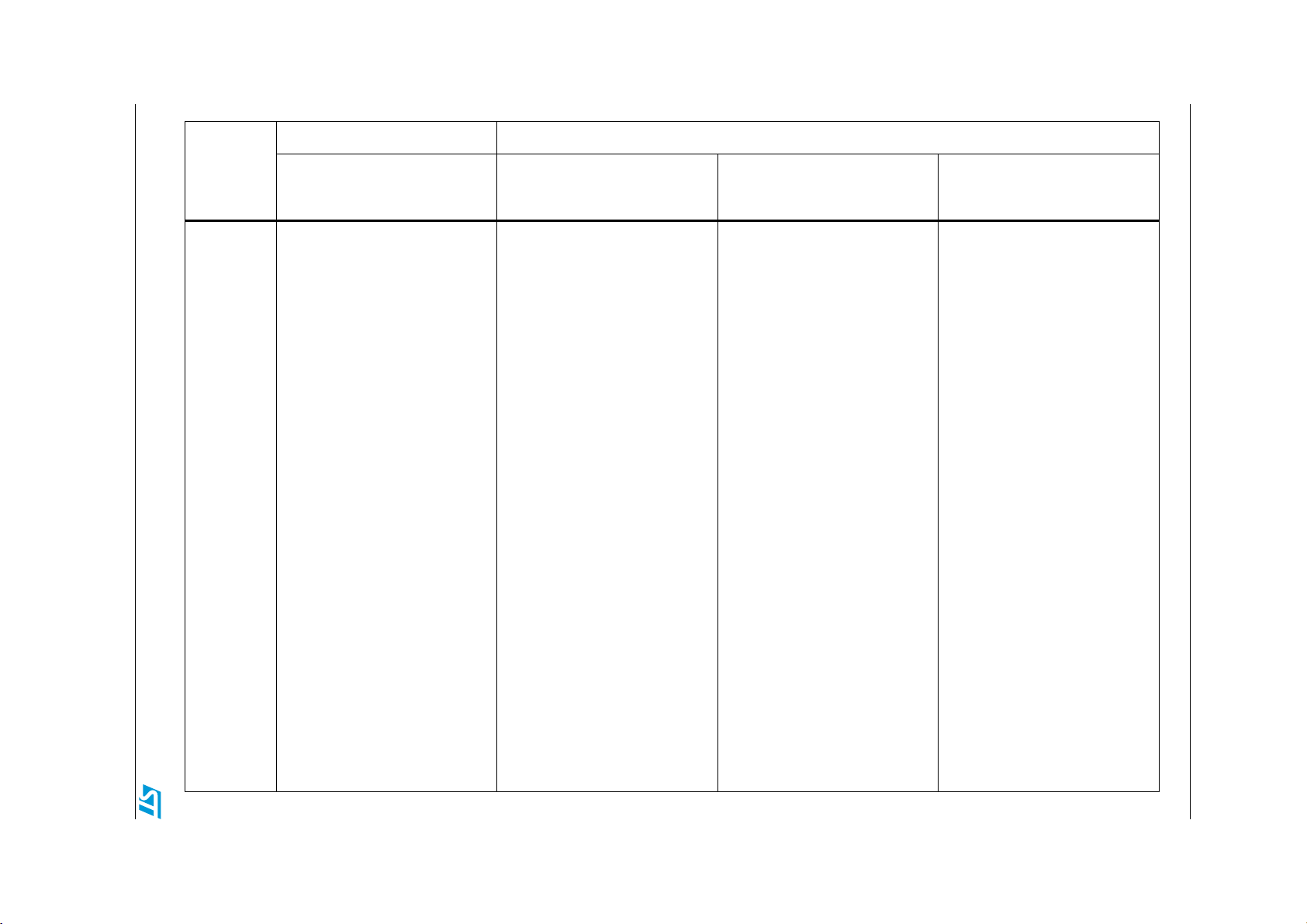
Table 1. Overview of STM8L family peripherals
Peripheral
RAM Up to 1.5 Kbytes Up to 2 Kbytes Up to 2 Kbytes Up to 4 Kbytes
Flash
Program
memory
STM8L10x STM8L15x/STM8L16x
Low density
STM8L10x
Up to 8 Kbytes From 4 to 8 Kbytes
Low density
STM8L15x
Medium
density
STM8L15x
From 16 to
32 Kbytes
Medium+/High density STM8L15x/
High density STM8L16x
32 Kbytes in medium+ density devices
64 Kbytes in high density devices
(STM8L15x/16x)
Doc ID 16993 Rev 3 7/63
Page 8
STM8L family compatibility AN3139
Table 1. Overview of STM8L family peripherals (continued)
STM8L10x STM8L15x/STM8L16x
Peripheral
Data
EEPROM
Interrupt
C L K Ye s Ye s Ye s Ye s
AWU Yes
RTC
B e e p Ye s Ye s Ye s Ye s
I W D G Ye s Ye s Ye s Ye s
WWDG Not available Yes Yes Yes
C O M P Ye s Ye s Yes Ye s
RI &
SYSCFG
Low density
STM8L10x
Up to 2 Kbytes in
Flash program
memory
Size configurable
by option byte
Up to 26 Peripheral
interrupt vectors
Not available Yes Yes Yes
Not available Yes Yes Yes
Low density
STM8L15x
Up to 1 Kbytes in
separate memory
array;
Fixed size
Up to 32 Peripheral
interrupt vectors
Not available Not available Not available
Medium
density
STM8L15x
Up to 1 Kbytes
in separate
memory array;
Fixed size
Up to 32
Peripheral
interrupt vectors
Medium+/High density STM8L15x/
High density STM8L16x
Up to 2 Kbytes in separate memory
Fixed size
Up to 32 Peripheral interrupt vectors
array;
GPIO
EXTI
DMA
ADC Not available ADC1 ADC1 ADC1
DAC
TIM
Infrared
Interface
IRTIM
I2C I2C I2C1 I2C1 I2C1
Up to 30I/Os
(GPIOA..D)
Up to 29 external
interrupt lines
Not available
Not available DAC1 channel DAC 1 channels DAC 2channels
Basic TIM4
General-purpose
TIM2/3
Ye s Ye s Ye s Ye s
Up to 41 I/Os
(GPIOA..F)
Up to 40 external
interrupt lines
DMA1 with 4
channels
Basic TIM4
General-purpose
TIM2/3
Up to 41 I/Os
(GPIOA..F)
Up to 40
external
interrupt lines
DMA1 with 4
channels
Basic TIM4
General-
purpose TIM2/3
Advanced-
control TIM1
Up to 68 I/Os (GPIOA..F) in high
density devices
Up to 67 external interrupt lines
DMA1 with 4 channels
Basic TIM4
General-purpose TIM2/3/5
Advanced-control TIM1
8/63 Doc ID 16993 Rev 3
Page 9
AN3139 STM8L family compatibility
Table 1. Overview of STM8L family peripherals (continued)
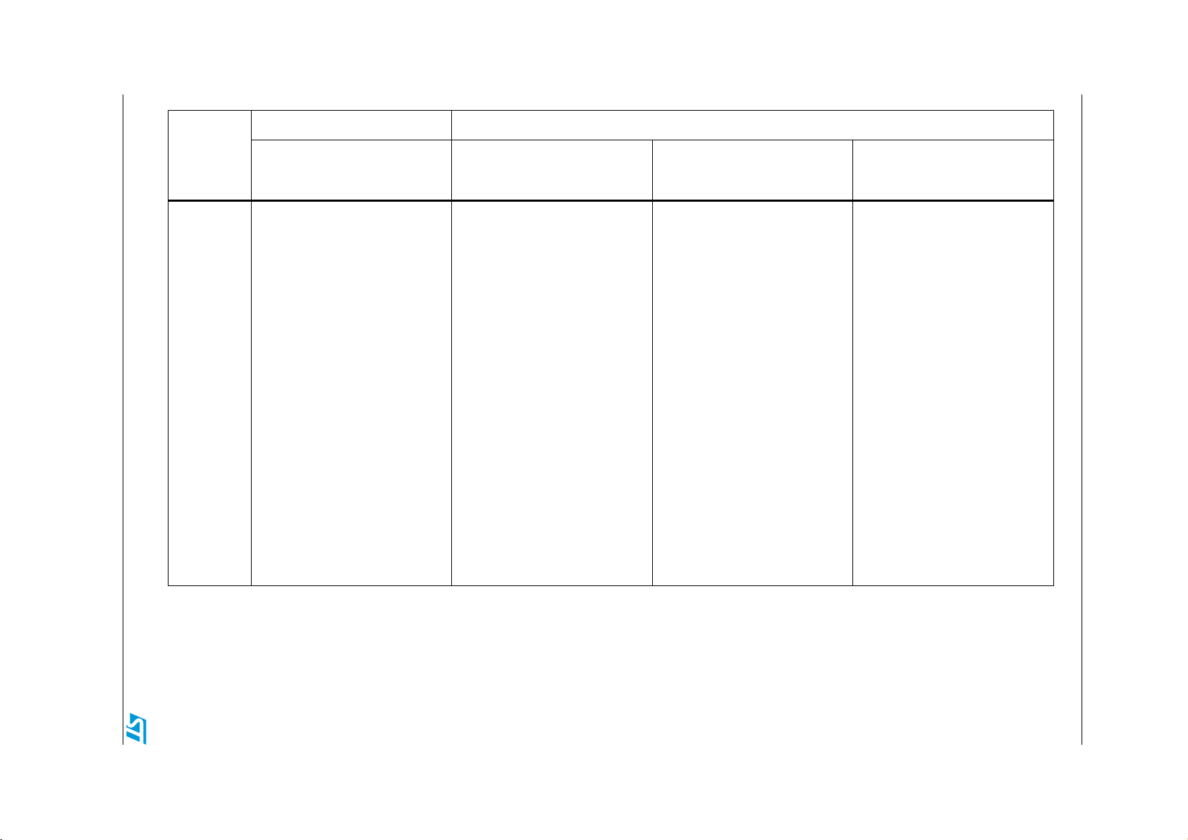
STM8L10x STM8L15x/STM8L16x
Peripheral
SPI SPI SPI1 SPI1 SPI1/SPI2
USART USART USART1 USART1 USART1/USART2/USART3
LCD Not available Yes Yes Yes
AES
1. Available on high-density STM8L16x devices only.
Low density
STM8L10x
Not available Not available Not available Yes
Low density
STM8L15x
Medium
density
STM8L15x
Medium+/High density STM8L15x/
High density STM8L16x
(1)
1.2 Fully compatible blocks
The STM8L family embeds a set of system blocks which are by definition common to all
products. Those blocks are identical, so they have the same structure, registers and control
bits. There is no need to perform any software change to keep the same functionality at the
application level after migration. When external components are needed (e.g. Vcap
capacitor) no change is required from one product to another. All the features and behaviors
remain the same. These blocks are shown in Figure 1: STM8L family block diagram.
Fully compatible parts and peripherals are:
● STM8 core
● Debug / SWIM module
● Power-on reset (POR)
● Voltage regulator
● Low speed internal RC (LSI)
● High speed internal RC (HSI)
● Independent watchdog
● Timers (TIM2, TIM3 and TIM4)
● IR (infrared interface)
1.3 Blocks that are compatible with minor exceptions
Some of the peripherals or functional blocks can have differences in their electrical
parameters, structure, registers, control bits or other minor aspects but not in their main
functionality.
Doc ID 16993 Rev 3 9/63
Page 10
STM8L family compatibility AN3139
Note: The RTC, ADC, DAC, DMA, WWDG, LCD, SPI2, USART2, USART3 and BootROM
peripherals are not available in STM8L10x devices.
SPI2, USART2 and USART3 are not available in low and medium density STM8L15x
devices.
The AES peripheral is available only in high density STM8L16x devices.
The AWU peripheral is not available in STM8L15x devices and is replaced by the RTC, so
this aspect can also be considered as an incompatibility.
The following functional blocks can be considered as compatible with only a few negligible
differences:
● GPIO (I/O capabilities)
● Interrupt management (interrupt vectors)
● Power control (wakeup from low power mode)
● I2C1 (true open drain)
● SPI1
● USART1
● Internal memories (Flash, SRAM, EEPROM)
You can find more details about these blocks in Chapter 3: Block-by-block compatibility
analysis. You can also refer to Figure 1: STM8L family block diagram.
1.4 Blocks that are compatible with significant exceptions
A few peripherals have additional features or less important functionalities compared to the
same peripheral in another STM8L sub-family. For these particular peripherals you have to
adapt the software drivers and check all possible hardware dependencies.
The peripheral and functional blocks in the following list are compatible with significant
exceptions. The package pinout is high on the list as this aspect requires special attention:
● Package pinout
● CLK
● COMP
● ADC
● DAC
● LCD
● RTC
You can find more details in Section 3: Block-by-block compatibility analysis. You can also
refer to Figure 1: STM8L family block diagram.
10/63 Doc ID 16993 Rev 3
Page 11
AN3139 STM8L family compatibility
)NTERNAL2#OSCILLATOR
-(Z
)NTERNAL2#OSCILLATOR
K(Z
%XTERNAL2#OSCILLATOR
-(Z
#/-0
34-#ORE
)/S
)NFRAREDINTERFACE
)NTERRUPTCONTROLLER
37)-DEBUGMODULE
%XTERNAL2#OSCILLATOR
K(Z
#LOCK
CONTROLLER
AND#33
2ESETBLOCK
6OLTAGEREGULATOR
0/2 0$2 "/2 06$
!DDRESSANDDATABUS
!DDRESSANDDATABUS
&LASH
MEMORY
2!-
MEMORY
4)-
%%02/-
MEMORY
"OOT2/-
MEMORY
)7$'
!75
$!#
!$#
,#$
24#
77$'
30)
30)
)#
$-!
&ULLYCOMPATIBLE
#OMPATIBLEWITHMINOREXCEPTIONS
#OMPATIBLEWITHSIGNIFICANTEXCEPTIONS
,EGEND
-36
53!24
53!24
53!24
4)-
4)-
!%3
Figure 1. STM8L family block diagram
1. LCD, ADC1, WWDG, RTC, DAC, DMA, Boot ROM and AWU are fully compatible but not present in all
STM8L devices.
1.5 Firmware library
The peripheral compatibility throughout STM8L MCU families promotes platform design and
eases significantly the migration from one product line to the other. The software support is
Doc ID 16993 Rev 3 11/63
Page 12

STM8L family compatibility AN3139
however essential during development time. Extensive software libraries are available for
both STM8L10x, STM8L15x and STM8L16x devices, providing the user with a hardware
abstraction layer (HAL) for all MCU resources. Moreover, there is not a single control/status
bit that is not covered by a C function or an API.
The software library covers three abstraction levels, and it includes:
1. A complete register address map with all bits, bit fields and registers declared in C. By
providing this map, the software library makes the designers’ task much lighter and,
even more importantly so, it gives all the benefits of a bug-free reference mapping file,
thus speeding up the early project phase.
2. A collection of routines and data structures in API form, that covers all peripheral
functions. This collection can directly be used as a reference framework, since it also
includes macros for supporting core-related intrinsic features and common constant
and data type definition. Moreover, it is compiler agnostic and can therefore be used
with any existing or future toolchain. It was developed using the MISRA C automotive
standard.
3. A set of examples covering all available peripherals (35 examples so far for the
STM8L10x sub-family, 35 for the STM8L15x sub-family), with template projects for the
most common development toolchains. With the appropriate hardware evaluation
board, only a few hours are needed to get started with a brand new microcontroller. It is
then up to you to choose how to use the library. You can either pick up the files useful
for the design, use examples to get trained or quickly evaluate the product. You can
also use the API to save development time.
Let us now have a look at the few key files and concepts. Two separate libraries support the
STM8L10x and STM8L15x devices. In the file names below, you simply need to replace the
“stm8l1xx_” prefix by “stm8l10x” or “stm8l15x” depending on the chosen product.
● stm8l1xx_.h
This file is the only header file that must be included in the C source code, usually in main.c.
This file contains:
– data structures and address mapping for all peripherals
– macros to access peripheral register hardware (for bit manipulation for instance),
plus STM8 core intrinsics
– a configuration section used to select the device implemented in the target
application. You also have the choice to use or not the peripheral drivers in the
application code (that is code based on direct access to registers rather than
through API drivers)
● stm8l1xx_conf.h
This is the peripheral driver configuration file, where you specify the peripherals you want to
use in your application, plus a few application-specific parameters such as the crystal frequency.
● stm8l1xxx_it.c
This file contains the template IRQ handler to be filled, but this is already the first
development step.
Once you have understood the above operating principle and file organization, for simple
applications, you could virtually switch from one product to the other without referring to the
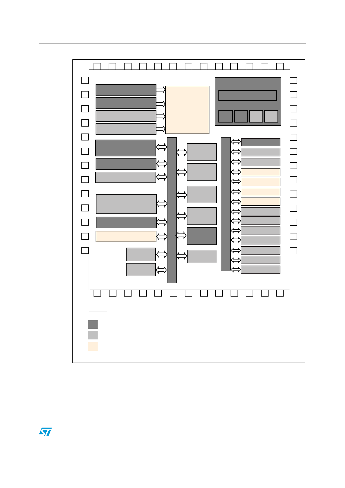
reference manual. Figure 2: STM8L10x code example and Figure 3: STM8L15x code exam-
ple show the initialization code (using the firmware library) for STM8L10x and STM8L15x
products, respectively.
12/63 Doc ID 16993 Rev 3
Page 13
AN3139 STM8L family compatibility
Figure 2. STM8L10x code example
Figure 3. STM8L15x code example
All parameters are identical, and the procedure is similar with two function calls for both configuration and startup.
The main difference is the additional peripherals of the same type that are added in the
STM8L15x sub-family:
● when migrating from STM8L10x sub-family to STM8L15x sub-family, the additional
peripheral must be added in every firmware library function as the first parameter (refer
to Figure 3)
● when migrating from STM8L15x sub-family to STM8L10x sub-family, the additional
peripheral given as the first parameter in every firmware library function must be
removed (refer to Figure 2)
Another difference in the SPI peripheral is the CRC capability which is supported only in the
STM8L15x devices. In the above example (Figure 3.), the CRC polynomial “0x07” is explicitly defined. This CRC polynomial parameter must be removed from the “init” function in the
case of a migration from the STM8L15x sub-family to the STM8L10x sub-family.
The following table shows an overview of the firmware library compatibility between the two
sub-families STM8L10x and STM8L15x/STM8L16x and between the different peripherals of
the STM8L15x/STM8L16x sub-family. It describes the differences in terms of:
1. New features like the IrDA, Smartcard, Halfduplex and DAC dual channel features
2. Common features but with different implementations, like the comparator and CLK
initialization.
Doc ID 16993 Rev 3 13/63
Page 14

STM8L family compatibility AN3139
To migrate from the STM8L10x sub-family to the STM8L15x/STM8L16x sub-family when
using the communication peripherals (SPI, I2C or USART), you have to add the additional
peripheral of the same type as the first parameter in every function used from the firmware
library. A full compatibility, in terms of function parameter names, is guaranteed for all
common features.
14/63 Doc ID 16993 Rev 3
Page 15
Table 2. STM8L firmware library compatibility
STM8L10x STM8L15x/STM8L16x
AN3139 STM8L family compatibility
Doc ID 16993 Rev 3 15/63
Peripheral
Flash
Low density STM8L10x Low density STM8L15x Medium density STM8L15x
Same API "/* New functions */
1/ void
FLASH_ProgramOptionByte(uint
16_t Address, uint8_t Data);
2/ void
FLASH_EraseOptionByte(uint16
_t Address);
3/ void
FLASH_PowerWaitModeConfig(FL
ASH_Power_TypeDef
FLASH_Power);
4/ void
FLASH_PowerRunModeConfig(FLA
SH_Power_TypeDef
FLASH_Power);
5/ FLASH_PowerStatus_TypeDef
FLASH_GetPowerStatus(void);
"
"/* New functions */
1/ void
FLASH_ProgramOptionByte(uint
16_t Address, uint8_t Data);
2/ void
FLASH_EraseOptionByte(uint16
_t Address);
3/ void
FLASH_PowerWaitModeConfig(FL
ASH_Power_TypeDef
FLASH_Power);
4/ void
FLASH_PowerRunModeConfig(FLA
SH_Power_TypeDef
FLASH_Power);
5/ FLASH_PowerStatus_TypeDef
FLASH_GetPowerStatus(void);
"
Medium+/High density
STM8L15x/ High density
STM8L16x
"/* New functions */
1/ void
FLASH_ProgramOptionByte(uint
16_t Address, uint8_t Data);
2/ void
FLASH_EraseOptionByte(uint16
_t Address);
3/ void
FLASH_PowerWaitModeConfig(FL
ASH_Power_TypeDef
FLASH_Power);
4/ void
FLASH_PowerRunModeConfig(FLA
SH_Power_TypeDef
FLASH_Power);
5/ FLASH_PowerStatus_TypeDef
FLASH_GetPowerStatus(void);
"
Page 16
16/63 Doc ID 16993 Rev 3
Table 2. STM8L firmware library compatibility (continued)
STM8L10x STM8L15x/STM8L16x
STM8L family compatibility AN3139
Peripheral
CLK
Low density STM8L10x Low density STM8L15x Medium density STM8L15x
"/* New functions */
1/ void
CLK_CCOCmd(FunctionalState
NewState);
2/ void
CLK_PeripheralClockConfig(CLK_Pe
ripheral_TypeDef CLK_Peripheral,
FunctionalState NewState);
3/ void
CLK_MasterPrescalerConfig(CLK_Ma
sterPrescaler_TypeDef
CLK_MasterPrescaler);
4/void
CLK_CCOConfig(CLK_Output_TypeDef
CLK_Output);
"
"/* New functions */
1/ void
CLK_HSICmd(FunctionalState
NewState);
2/ void
CLK_AdjustHSICalibrationValue(ui
nt8_t CLK_HSICalibrationValue);
3/ void
CLK_LSICmd(FunctionalState
NewState);
4/ void
CLK_HSEConfig(CLK_HSE_TypeDef
CLK_HSE);
5/ void
CLK_LSEConfig(CLK_LSE_TypeDef
CLK_LSE);
6/ void
CLK_SYSCLKSourceConfig(CLK_SYSCL
KSource_TypeDef
CLK_SYSCLKSource);
7/ void
CLK_SYSCLKDivConfig(CLK_SYSCLKDi
v_TypeDef CLK_SYSCLKDiv);
8/ void
CLK_SYSCLKSourceSwitchCmd(Functi
onalState NewState);
9/ CLK_SYSCLKSource_TypeDef
CLK_GetSYSCLKSource(void);
10/ void
CLK_ClockSecuritySystemEnable(vo
id);CLK_BEEPCLKSource);
11/ void
CLK_ITConfig(CLK_IT_TypeDef
CLK_IT, FunctionalState
NewState);
"/* New functions */
1/ void
CLK_HSICmd(FunctionalState
NewState);
2/ void
CLK_AdjustHSICalibrationValue(ui
nt8_t CLK_HSICalibrationValue);
3/ void
CLK_LSICmd(FunctionalState
NewState);
4/ void
CLK_HSEConfig(CLK_HSE_TypeDef
CLK_HSE);
5/ void
CLK_LSEConfig(CLK_LSE_TypeDef
CLK_LSE);
6/ void
CLK_SYSCLKSourceConfig(CLK_SYSCL
KSource_TypeDef
CLK_SYSCLKSource);
7/ void
CLK_SYSCLKDivConfig(CLK_SYSCLKDi
v_TypeDef CLK_SYSCLKDiv);
8/ void
CLK_SYSCLKSourceSwitchCmd(Functi
onalState NewState);
9/ CLK_SYSCLKSource_TypeDef
CLK_GetSYSCLKSource(void);
10/ void
CLK_ClockSecuritySystemEnable(vo
id);
11/ void
CLK_ITConfig(CLK_IT_TypeDef
CLK_IT, FunctionalState
NewState);
Medium+/High density
STM8L15x/ High density
STM8L16x
"/* New functions */
1/ void
CLK_HSICmd(FunctionalState
NewState);
2/ void
CLK_AdjustHSICalibrationValue(ui
nt8_t CLK_HSICalibrationValue);
3/ void
CLK_LSICmd(FunctionalState
NewState);
4/ void
CLK_HSEConfig(CLK_HSE_TypeDef
CLK_HSE);
5/ void
CLK_LSEConfig(CLK_LSE_TypeDef
CLK_LSE);
6/ void
CLK_SYSCLKSourceConfig(CLK_SYSCL
KSource_TypeDef
CLK_SYSCLKSource);
7/ void
CLK_SYSCLKDivConfig(CLK_SYSCLKDi
v_TypeDef CLK_SYSCLKDiv);
8/ void
CLK_SYSCLKSourceSwitchCmd(Functi
onalState NewState);
9/ CLK_SYSCLKSource_TypeDef
CLK_GetSYSCLKSource(void);
10/ void
CLK_ClockSecuritySystemEnable(vo
id);
11/ void
CLK_ITConfig(CLK_IT_TypeDef
CLK_IT, FunctionalState
NewState);
"
Page 17
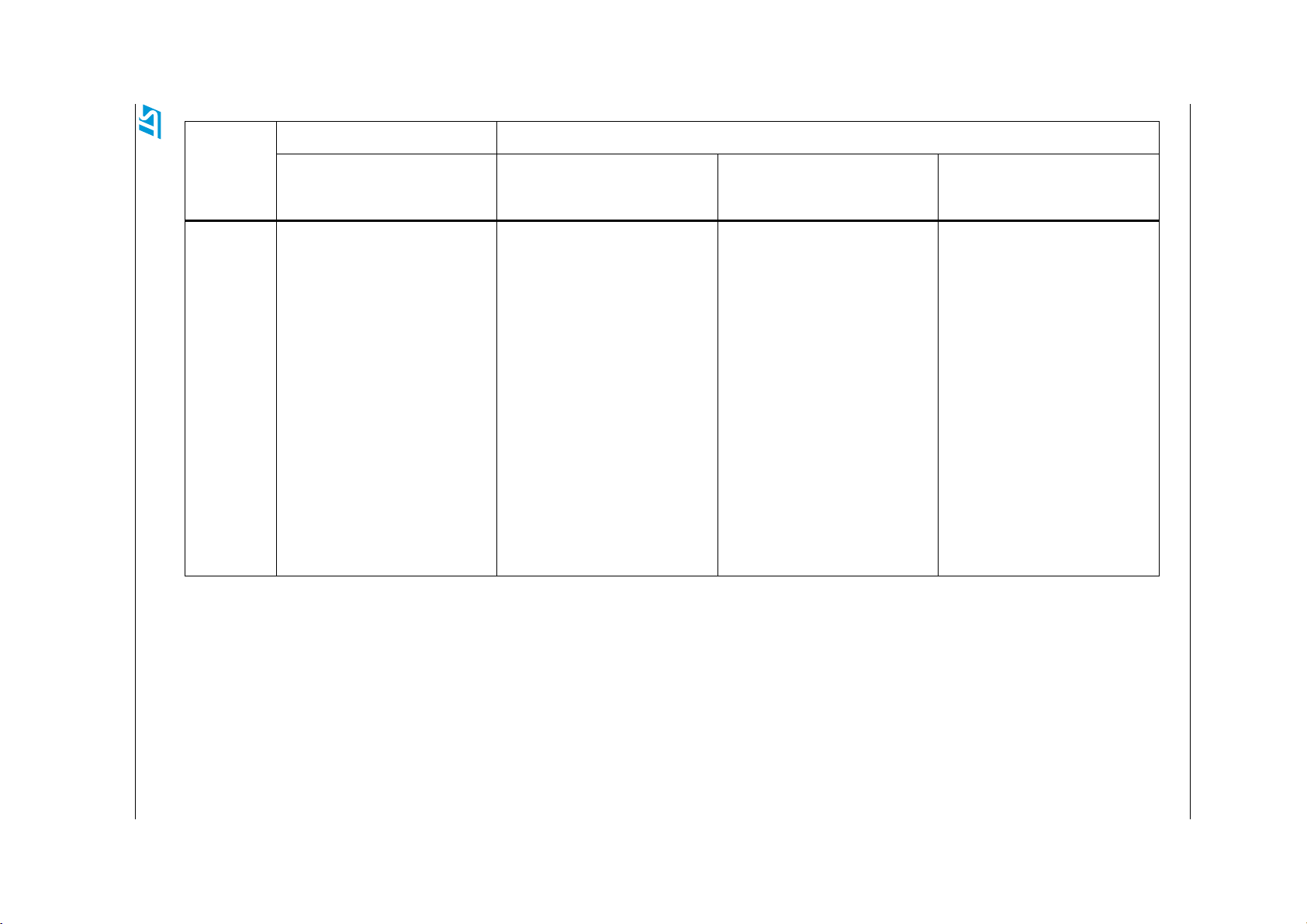
Table 2. STM8L firmware library compatibility (continued)
STM8L10x STM8L15x/STM8L16x
AN3139 STM8L family compatibility
Doc ID 16993 Rev 3 17/63
Peripheral
CLK
Low density STM8L10x Low density STM8L15x Medium density STM8L15x
12/ void
CLK_CCOConfig(CLK_CCOSource_Type
Def CLK_CCOSource,
CLK_CCODiv_TypeDef CLK_CCODiv);
13/ void
CLK_RTCClockConfig(CLK_RTCCLKSou
rce_TypeDef CLK_RTCCLKSource,
CLK_RTCCLKDiv_TypeDef
CLK_RTCCLKDiv);
14/ void
CLK_BEEPClockConfig(CLK_BEEPCLKS
ource_TypeDef
15/ void
CLK_PeripheralClockConfig(CLK_Pe
ripheral_TypeDef CLK_Peripheral,
FunctionalState NewState);
16/ void
CLK_LSEClockSecuritySystemEnable
(void);
17/ void
CLK_RTCCLKSwitchOnLSEFailureEnab
le(void);"
12/ void
CLK_CCOConfig(CLK_CCOSource_Type
Def CLK_CCOSource,
CLK_CCODiv_TypeDef CLK_CCODiv);
13/ void
CLK_RTCClockConfig(CLK_RTCCLKSou
rce_TypeDef CLK_RTCCLKSource,
CLK_RTCCLKDiv_TypeDef
CLK_RTCCLKDiv);
14/ void
CLK_BEEPClockConfig(CLK_BEEPCLKS
ource_TypeDef
CLK_BEEPCLKSource);
15/ void
CLK_PeripheralClockConfig(CLK_Pe
ripheral_TypeDef CLK_Peripheral,
FunctionalState NewState);
"
Medium+/High density
STM8L15x/ High density
STM8L16x
12/ void
CLK_CCOConfig(CLK_CCOSource_Type
Def CLK_CCOSource,
CLK_CCODiv_TypeDef CLK_CCODiv);
13/ void
CLK_RTCClockConfig(CLK_RTCCLKSou
rce_TypeDef CLK_RTCCLKSource,
CLK_RTCCLKDiv_TypeDef
CLK_RTCCLKDiv);
14/ void
CLK_BEEPClockConfig(CLK_BEEPCLKS
ource_TypeDef
CLK_BEEPCLKSource);
15/ void
CLK_PeripheralClockConfig(CLK_Pe
ripheral_TypeDef CLK_Peripheral,
FunctionalState NewState);
16/ void
CLK_LSEClockSecuritySystemEnable
(void);
17/ void
CLK_RTCCLKSwitchOnLSEFailureEnab
le(void);
Page 18
18/63 Doc ID 16993 Rev 3
Table 2. STM8L firmware library compatibility (continued)
STM8L10x STM8L15x/STM8L16x
STM8L family compatibility AN3139
Peripheral
COMP
Low density STM8L10x Low density STM8L15x Medium density STM8L15x
"/*Updated functions*/
1/ void
COMP_Init(COMP_Selection_TypeDef
COMP_Selection,
COMP_Reference_TypeDef
COMP_Reference,
COMP_Polarity_TypeDef
COMP_Polarity);
2/ void COMP_Cmd(FunctionalState
NewState);
3/ void
COMP_SelectionConfig(COMP_Select
ion_TypeDef COMP_Selection,
FunctionalState NewState);
4/ void
COMP_ITConfig(COMP_IT_TypeDef
COMP_IT,
FunctionalState NewState);
5/ void
COMP_TIM2Config(COMP_TIM2Config_
TypeDef COMP_TIM2Config);
6/ void
COMP_SwitchConfig(COMP_Switch_Ty
peDef COMP_Switch,
FunctionalState NewState);
"/*Updated functions*/
1/ void
COMP_Init(COMP_InvertingInput_Ty
pedef COMP_InvertingInput,
COMP_OutputSelect_Typedef
COMP_OutputSelect,
COMP_Speed_TypeDef COMP_Speed);
2/ void
COMP_VrefintToCOMP1Connect(Funct
ionalState NewState);
3/ void
COMP_EdgeConfig(COMP_Selection_T
ypeDef COMP_Selection,
COMP_Edge_TypeDef COMP_Edge);
4/ COMP_OutputLevel_TypeDef
COMP_GetOutputLevel(COMP_Selecti
on_TypeDef COMP_Selection);
5/ void
COMP_WindowCmd(FunctionalState
NewState);
6/ void
COMP_ITConfig(COMP_Selection_Typ
eDef COMP_Selection,
FunctionalState NewState);
Medium+/High density
STM8L15x/ High density
STM8L16x
"/*Updated functions*/
1/ void
COMP_Init(COMP_InvertingInput_Ty
pedef COMP_InvertingInput,
COMP_OutputSelect_Typedef
COMP_OutputSelect,
COMP_Speed_TypeDef COMP_Speed);
2/ void
COMP_VrefintToCOMP1Connect(Funct
ionalState NewState);
3/ void
COMP_EdgeConfig(COMP_Selection_T
ypeDef COMP_Selection,
COMP_Edge_TypeDef COMP_Edge);
4/ COMP_OutputLevel_TypeDef
COMP_GetOutputLevel(COMP_Selecti
on_TypeDef COMP_Selection);
5/ void
COMP_WindowCmd(FunctionalState
NewState);
6/ void
COMP_ITConfig(COMP_Selection_Typ
eDef COMP_Selection,
FunctionalState NewState);
Page 19
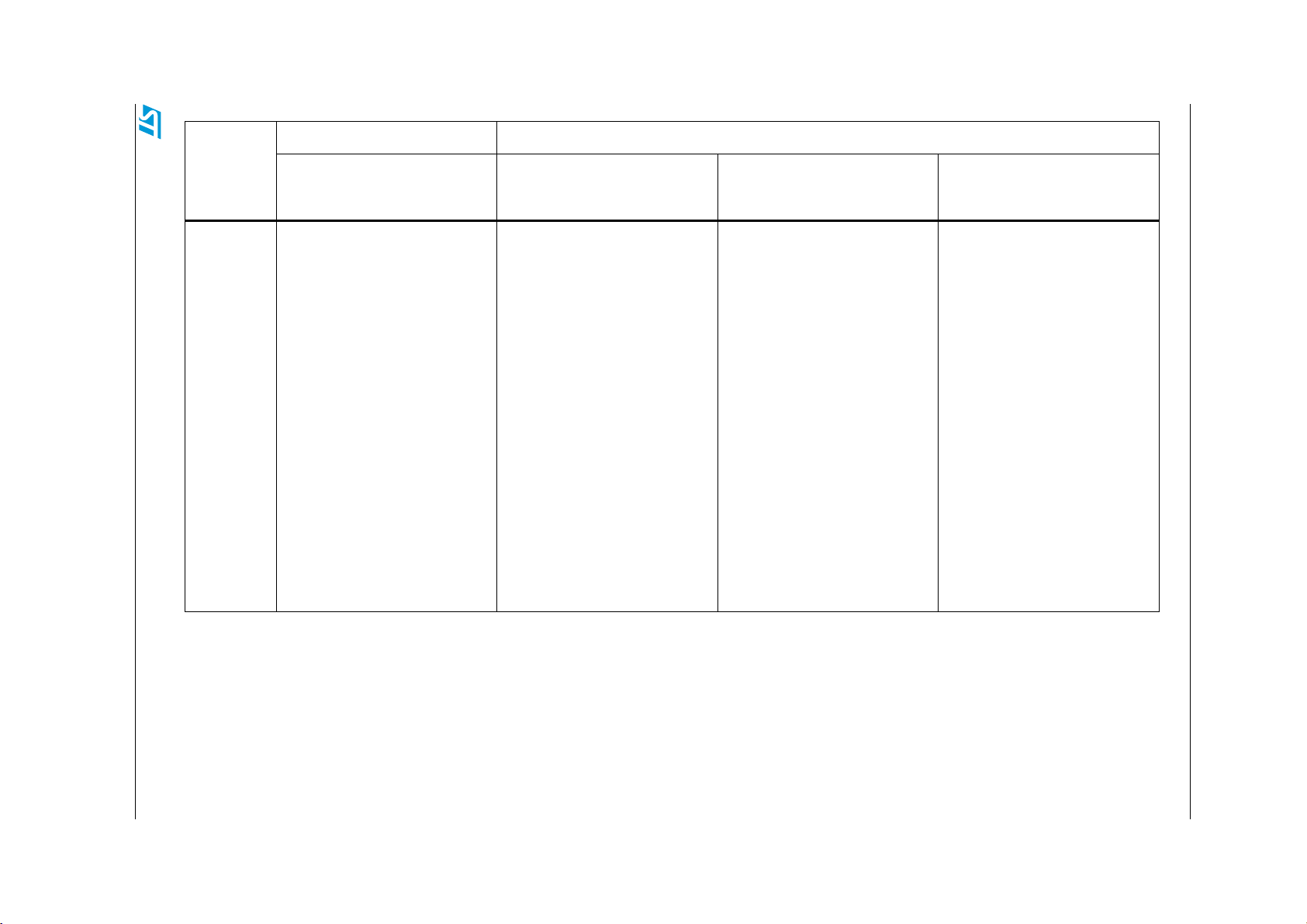
Table 2. STM8L firmware library compatibility (continued)
STM8L10x STM8L15x/STM8L16x
AN3139 STM8L family compatibility
Doc ID 16993 Rev 3 19/63
Peripheral
COMP
Low density STM8L10x Low density STM8L15x Medium density STM8L15x
7/ void
COMP_TIMConnect(COMP_TimersConne
ction_TypeDef
COMP_TIMConnection);
8/ void
COMP_SelectPolarity(COMP_Polarit
y_TypeDef COMP_Polarity);
9/ void
COMP_SetReference(COMP_Reference
_TypeDef COMP_Reference);
10/ FlagStatus
COMP_GetOutputStatus(COMP_Output
_TypeDef COMP_Output);
11/ FlagStatus
COMP_GetFlagStatus(COMP_FLAG_Typ
eDef COMP_Flag);"
7/ void
COMP_TriggerConfig(COMP_TriggerG
roup_TypeDef COMP_TriggerGroup,
COMP_TriggerPin_TypeDef
COMP_TriggerPin,
FunctionalState NewState);
8/ void
COMP_VrefintOutputCmd(Functional
State NewState);
9/ void
COMP_SchmittTriggerCmd(Functiona
lState NewState);
10/ FlagStatus
COMP_GetFlagStatus(COMP_Selectio
n_TypeDef COMP_Selection);
11/ void
COMP_ClearFlag(COMP_Selection_Ty
peDef COMP_Selection);
12/ ITStatus
COMP_GetITStatus(COMP_Selection_
TypeDef COMP_Selection);
13/ void
COMP_ClearITPendingBit(COMP_Sele
ction_TypeDef COMP_Selection);"
Medium+/High density
STM8L15x/ High density
STM8L16x
7/ void
COMP_TriggerConfig(COMP_TriggerG
roup_TypeDef COMP_TriggerGroup,
COMP_TriggerPin_TypeDef
COMP_TriggerPin,
FunctionalState NewState);
8/ void
COMP_VrefintOutputCmd(Functional
State NewState);
9/ void
COMP_SchmittTriggerCmd(Functiona
lState NewState);
10/ FlagStatus
COMP_GetFlagStatus(COMP_Selectio
n_TypeDef COMP_Selection);
11/ void
COMP_ClearFlag(COMP_Selection_Ty
peDef COMP_Selection);
12/ ITStatus
COMP_GetITStatus(COMP_Selection_
TypeDef COMP_Selection);
13/ void
COMP_ClearITPendingBit(COMP_Sele
ction_TypeDef COMP_Selection);"
Page 20

20/63 Doc ID 16993 Rev 3
Table 2. STM8L firmware library compatibility (continued)
STM8L10x STM8L15x/STM8L16x
STM8L family compatibility AN3139
Peripheral
I2C1
Low density STM8L10x Low density STM8L15x Medium density STM8L15x
Same API /* New functions */
1/ void I2C_DMACmd(I2C_TypeDef*
I2Cx, FunctionalState NewState);
2/ void
I2C_DMALastTransferCmd(I2C_TypeD
ef* I2Cx, FunctionalState
NewState);
3/ void I2C_ARPCmd(I2C_TypeDef*
I2Cx, FunctionalState NewState);
4/ void
I2C_SMBusAlertConfig(I2C_TypeDef
* I2Cx, I2C_SMBusAlert_TypeDef
I2C_SMBusAlert);
5/ void
I2C_PECPositionConfig(I2C_TypeDe
f* I2Cx, I2C_PECPosition_TypeDef
I2C_PECPosition);
6/ void
I2C_TransmitPEC(I2C_TypeDef*
I2Cx, FunctionalState NewState);
7/ void
I2C_CalculatePEC(I2C_TypeDef*
I2Cx, FunctionalState NewState);
.
.
.
/* New functions */
1/ void I2C_DMACmd(I2C_TypeDef*
I2Cx, FunctionalState NewState);
2/ void
I2C_DMALastTransferCmd(I2C_TypeD
ef* I2Cx, FunctionalState
NewState);
3/ void I2C_ARPCmd(I2C_TypeDef*
I2Cx, FunctionalState NewState);
4/ void
I2C_SMBusAlertConfig(I2C_TypeDef
* I2Cx, I2C_SMBusAlert_TypeDef
I2C_SMBusAlert);
5/ void
I2C_PECPositionConfig(I2C_TypeDe
f* I2Cx, I2C_PECPosition_TypeDef
I2C_PECPosition);
6/ void
I2C_TransmitPEC(I2C_TypeDef*
I2Cx, FunctionalState NewState);
7/ void
I2C_CalculatePEC(I2C_TypeDef*
I2Cx, FunctionalState NewState);
.
.
.
Medium+/High density
STM8L15x/ High density
STM8L16x
/* New functions */
1/ void I2C_DMACmd(I2C_TypeDef*
I2Cx, FunctionalState NewState);
2/ void
I2C_DMALastTransferCmd(I2C_TypeD
ef* I2Cx, FunctionalState
NewState);
3/ void I2C_ARPCmd(I2C_TypeDef*
I2Cx, FunctionalState NewState);
4/ void
I2C_SMBusAlertConfig(I2C_TypeDef
* I2Cx, I2C_SMBusAlert_TypeDef
I2C_SMBusAlert);
5/ void
I2C_PECPositionConfig(I2C_TypeDe
f* I2Cx, I2C_PECPosition_TypeDef
I2C_PECPosition);
6/ void
I2C_TransmitPEC(I2C_TypeDef*
I2Cx, FunctionalState NewState);
7/ void
I2C_CalculatePEC(I2C_TypeDef*
I2Cx, FunctionalState NewState);
.
.
.
Page 21

Table 2. STM8L firmware library compatibility (continued)
STM8L10x STM8L15x/STM8L16x
AN3139 STM8L family compatibility
Doc ID 16993 Rev 3 21/63
Peripheral
SPIx
Low density STM8L10x Low density STM8L15x Medium density STM8L15x
"/*Updated functions*/
1/ void
SPI_Init(SPI_FirstBit_TypeDef
SPI_FirstBit,
SPI_BaudRatePrescaler_TypeDef
SPI_BaudRatePrescaler,
SPI_Mode_TypeDef SPI_Mode,
SPI_CPOL_TypeDef SPI_CPOL,
SPI_CPHA_TypeDef SPI_CPHA,
SPI_DirectionMode_TypeDef
SPI_Data_Direction,
SPI_NSS_TypeDef
SPI_Slave_Management);"
"/* New functions */
1/ void
SPI_TransmitCRC(SPI_TypeDef*
SPIx);
2/ void
SPI_CalculateCRCCmd(SPI_TypeDef*
SPIx, FunctionalState NewState);
3/ uint8_t
SPI_GetCRC(SPI_TypeDef* SPIx,
SPI_CRC_TypeDef SPI_CRC);
4/ void
SPI_ResetCRC(SPI_TypeDef* SPIx);
5/ uint8_t
SPI_GetCRCPolynomial(SPI_TypeDef
* SPIx);
6/ void SPI_DMACmd(SPI_TypeDef*
SPIx, SPI_DMAReq_TypeDef
SPI_DMAReq, FunctionalState
NewState);
Medium+/High density
STM8L15x/ High density
STM8L16x
"/* New functions */
1/ void
SPI_TransmitCRC(SPI_TypeDef*
SPIx);
2/ void
SPI_CalculateCRCCmd(SPI_TypeDef*
SPIx, FunctionalState NewState);
3/ uint8_t
SPI_GetCRC(SPI_TypeDef* SPIx,
SPI_CRC_TypeDef SPI_CRC);
4/ void
SPI_ResetCRC(SPI_TypeDef* SPIx);
5/ uint8_t
SPI_GetCRCPolynomial(SPI_TypeDef
* SPIx);
6/ void SPI_DMACmd(SPI_TypeDef*
SPIx, SPI_DMAReq_TypeDef
SPI_DMAReq, FunctionalState
NewState);
Page 22

22/63 Doc ID 16993 Rev 3
Table 2. STM8L firmware library compatibility (continued)
STM8L10x STM8L15x/STM8L16x
STM8L family compatibility AN3139
Peripheral
Low density STM8L10x Low density STM8L15x Medium density STM8L15x
/*Updated functions*/
1/ void SPI_Init(SPI_TypeDef*
SPIx, SPI_FirstBit_TypeDef
SPI_FirstBit,
SPI_BaudRatePrescaler_TypeDef
SPI_BaudRatePrescaler,
SPI_Mode_TypeDef SPI_Mode,
SPI_CPOL_TypeDef SPI_CPOL,
SPI_CPHA_TypeDef SPI_CPHA,
SPI_DirectionMode_TypeDef
SPI_Data_Direction,
SPI_NSS_TypeDef
SPI_Slave_Management, uint8_t
CRCPolynomial);"
Medium+/High density
STM8L15x/ High density
STM8L16x
/*Updated functions*/
1/ void SPI_Init(SPI_TypeDef*
SPIx, SPI_FirstBit_TypeDef
SPI_FirstBit,
SPI_BaudRatePrescaler_TypeDef
SPI_BaudRatePrescaler,
SPI_Mode_TypeDef SPI_Mode,
SPI_CPOL_TypeDef SPI_CPOL,
SPI_CPHA_TypeDef SPI_CPHA,
SPI_DirectionMode_TypeDef
SPI_Data_Direction,
SPI_NSS_TypeDef
SPI_Slave_Management, uint8_t
CRCPolynomial);"
Page 23

Table 2. STM8L firmware library compatibility (continued)
STM8L10x STM8L15x/STM8L16x
AN3139 STM8L family compatibility
Doc ID 16993 Rev 3 23/63
Peripheral
USARTx
Low density STM8L10x Low density STM8L15x Medium density STM8L15x
"/* New functions */
1/ void
USART_HalfDuplexCmd(USART_TypeDe
f* USARTx, FunctionalState
NewState);
2/ void
USART_IrDAConfig(USART_TypeDef*
USARTx, USART_IrDAMode_TypeDef
USART_IrDAMode);
3/ void
USART_IrDACmd(USART_TypeDef*
USARTx, FunctionalState
NewState);
4/ void
USART_SmartCardCmd(USART_TypeDef
* USARTx, FunctionalState
NewState);
5/ void
USART_SmartCardNACKCmd(USART_Typ
eDef* USARTx, FunctionalState
NewState);
6/ void
USART_SetGuardTime(USART_TypeDef
* USARTx, uint8_t
USART_GuardTime);
7/ void
USART_SetPrescaler(USART_TypeDef
* USARTx, uint8_t
USART_Prescaler);"
Medium+/High density
STM8L15x/ High density
STM8L16x
"/* New functions */
1/ void
USART_HalfDuplexCmd(USART_TypeDe
f* USARTx, FunctionalState
NewState);
2/ void
USART_IrDAConfig(USART_TypeDef*
USARTx, USART_IrDAMode_TypeDef
USART_IrDAMode);
3/ void
USART_IrDACmd(USART_TypeDef*
USARTx, FunctionalState
NewState);
4/ void
USART_SmartCardCmd(USART_TypeDef
* USARTx, FunctionalState
NewState);
5/ void
USART_SmartCardNACKCmd(USART_Typ
eDef* USARTx, FunctionalState
NewState);
6/ void
USART_SetGuardTime(USART_TypeDef
* USARTx, uint8_t
USART_GuardTime);
7/ void
USART_SetPrescaler(USART_TypeDef
* USARTx, uint8_t
USART_Prescaler);"
ITC Same API Same API Same API Same API
PWR
Not available Same API Same API Same API
WFE Same API Same API Same API Same API
RST Same API Same API Same API Same API
GPIO Same API Same API Same API Same API
EXTI Same API Same API Same API Same API
DMA1
Not available Same API Same API Same API
Page 24

24/63 Doc ID 16993 Rev 3
Table 2. STM8L firmware library compatibility (continued)
STM8L10x STM8L15x/STM8L16x
STM8L family compatibility AN3139
Peripheral
Low density STM8L10x Low density STM8L15x Medium density STM8L15x
Medium+/High density
STM8L15x/ High density
ADC1 Not available Same API Same API Same API
"/* New functions */
1/ void
DAC_DualSoftwareTriggerCmd(Funct
ionalState NewState);
2/ void
DAC_WaveGenerationCmd(DAC_Channe
l_TypeDef DAC_Channel,
DAC_Wave_TypeDef DAC_Wave,
FunctionalState NewState);
3/ void
DAC_SetNoiseWaveLFSR(DAC_Channel
_TypeDef DAC_Channel,
DAC_LFSRUnmask_TypeDef
DAC Not available Same API Same API
DAC_LFSRUnmask);
4/ void
DAC_SetTriangleWaveAmplitude(DAC
_Channel_TypeDef DAC_Channel,
DAC_TriangleAmplitude_TypeDef
DAC_TriangleAmplitude);
5/ void
DAC_SetChannel2Data(DAC_Align_Ty
peDef DAC_Align, uint16_t
DAC_Data);
6/ void
DAC_SetDualChannelData(DAC_Align
_TypeDef DAC_Align, uint16_t
DAC_Data2, uint16_t DAC_Data1);"
STM8L16x
IRTIM Same API Same API Same Peripheral Same API
TIM1
Not available Not available Same Peripheral Same API
TIM2/3/4 Same API Same API Same Peripheral Same API
TIM5 Not available Not available Not available New Peripheral
AWU Same API
RTC
Not available Please refer to the AN3133 application note (Using the STM8L15x/STM8L16x real time clock).
Not available Not available Not available
BEEP Same API Same API Same API Same API
Page 25

Table 2. STM8L firmware library compatibility (continued)
STM8L10x STM8L15x/STM8L16x
AN3139 STM8L family compatibility
Doc ID 16993 Rev 3 25/63
Peripheral
Low density STM8L10x Low density STM8L15x Medium density STM8L15x
WWDG Not available Same API Same API Same API
IWDG Same API Same API Same API Same API
SYSCFG
AES
Not available Same API Same API Same API
Not available Not available Not available New Peripheral
Medium+/High density
STM8L15x/ High density
STM8L16x
Page 26

Planning for migration AN3139
2 Planning for migration
To migrate your application from one sub-family to another, you have to analyze the hardware migration as well as the application resources and firmware migration.
2.1 Hardware migration
If you use the same package and the same pin numbers, you can use the same PCB without any modification. All sub-families are pin-to-pin compatible.
2.2 Application resources and firmware migration
You have to analyze the compatibility level of your peripherals between the initial sub-family
and the new sub-family in the following cases:
● If you use the same resources and peripherals of the same type
– you do not have to modify anything in your code except the clock configuration
(Example: TIMx)
● If you use the same resources and different peripherals of the same type
– If one peripheral of the same type is not present any more, you can change the
reference to this peripheral and all related features (pin, clock and interrupt
configuration).
● If you use new resources and/or new peripherals of the same type
– If you need to migrate the application from STM8L10x devices to STM815x
devices without using the new peripherals, the user software can be kept as is
without any modification except the clock configuration. Using the standard
Peripherals library has several advantages: it saves coding time while
simultaneously reducing application development and integration costs.
The following table explains how to migrate from one sub-family to another and from one
package to another.
The table is intended to be used as follows:
● Sub-families or devices within the family are listed in rows. Moving between the rows
means changing the sub-family or changing the device.
● Available package sizes are listed in columns. Moving between columns means
changing the pin-count.
● The gray fields represent the migration between each column or row and give the
impacted features.
The impact of moves between two subfamilies is common for all available package pairs.
Therefore all gray cells in rows are merged into common fields. The text in these common
fields is as follows:
● When migrating downwards: the row between both sub-families lists the features that
are lost due to the migration.
● When migrating upwards, the row between both sub-families lists the features that are
added due to the migration.
26/63 Doc ID 16993 Rev 3
Page 27

AN3139 Planning for migration
A move to the right towards smaller packages mainly leads to a loss of I/O pins. So the
content of these cells is a simple list of impacted items only.
This section mainly discusses cases of migration between neighboring pairs. However, your
project may be a migration over several rows or columns in Ta bl e 3 or even in a diagonal
direction. In this case, you should check the differences indicated in each step passed by
the vertical and horizontal moves through the following table.
Doc ID 16993 Rev 3 27/63
Page 28

Planning for migration AN3139
Table 3. STM8L family migration products
Pin-count
20 28 32 48 64 80
STM8L10x
Low-density
Pin-to-pin
compatible
Pin-to-pin
compatible
RTC
+ADC
+COMP
Pin-to-pin
compatible
Pin-to-pin
compatible
Low-density
Pin-to-pin
compatible
+ TIM1
Pin-to-pin
compatible
RTC + ADC
+COMP
Pin-to-pin
compatible
+ TIM1+
LCD
Pin-topin
compati
ble
Pin-to-pin
compatible
+
TIM1+LCD
Functionality
Medium-density
STM8L15x/STM8L16x
Medium+ and High density
Pin-to-pin
compatible
+ LCD
Pin-topin
compati
ble
Pin-to-pin
compatible
+TIM5,
SPI2,
USART2,
USART3,
AES
Pin-topin
compati
ble
Pin-topin
compa
tible
28/63 Doc ID 16993 Rev 3
Page 29

AN3139 Block-by-block compatibility analysis
3 Block-by-block compatibility analysis
3.1 Package pinout
The following table gives an overview of the available packages in each STM8L family
Table 4. Overview of STM8L family packages
STM8L10x STM8L15x/STM8L16x
Medium+/High
Package
Low density STM8L10x
Low density
STM8L15x
Medium density
STM8L15x
density
STM8L15x/ High
density
STM8L16x
LQFP80
LQFP64
UFQFPN48 Not available Not available Not available x
LQFP48 Not available x x x
LQFP32 x
VFQFPN48
WFQFPN32 Not available Not available x Not available
WFQFPN28
UFQFPN28 Not available x x Not available
UFQFPN32 x x
UFQFPN28 x x
UFQFPN28 x x Not available Not available
Not available Not available Not available x
Not available Not available Not available x
Not available x Not available
Not available Not available x Not available
Not available Not available x Not available
Not available Not available
Not available Not available
UFQFPN20 x x Not available Not available
UFQFPN20 Not available x Not available Not available
3.1.1 Digital power supply
The digital power supply design includes two supply sources. The purpose is to distribute
the current flowing through the I/O logic separately from the rest of the digital microcontroller
Doc ID 16993 Rev 3 29/63
Page 30

Block-by-block compatibility analysis AN3139
circuits. Up to two V
DDIO
/ V
pin pairs are used as well as the main VDD / VSS digital
SSIO
supply pair, depending on the pin-count:
● Both V
pairs are present in the 48-pin package in the STM8L15x/STM8L16x sub-
DDIO
family.
● Only one V
pin is available to supply power to the I/Os in the STM8L10x and
DDIO
STM8L15x/STM8L16x sub-families from 32-pin packages to 20-pin packages.
The total output current is limited by the number of supply pins. The total output current
capability declines for smaller packages, regardless of the number of I/Os with high-sink
capability.
In the medium, medium+ and high density STM8L15x/STM8L16x devices,, the V
connecting the external voltage source for the LCD is present on the 48-pin and 32-pin
packages when the LCD is available.
3.1.2 ADC power supply and voltage reference
The analog power supply design includes an extra power supply for the analog parts of the
microcontroller and an external reference voltage connected via an extra pin pair.
● The V
DDA/VSSA
and 48-pin packages in the STM8L15x/STM8L16x sub-family. Without these pins, it is
not possible to use the ADC zooming function feature (see Section 3.4: ADC modes for
more details).
● For the rest of the STM8L15x/STM8L16x sub-family (32-pin package) the ADC
reference is taken from the main analog supply V
Note: As the ADC is not present in the STM8L10x family, V
supply pins are not available on packages for this family.
and the V
REF+/VREF-
analog supply pin pair are present on the 28-pin
.
DDA
DDA/VSSA
and V
REF+/VREF
pin for
LCD
analog
3.1.3 Alternate functions
The main purpose of the alternate feature concept is to keep the microcontroller
configurable for different user and application needs. This is especially important and useful
in low pin-count packages.
Default alternate functions can be enabled on dedicated pins by settings in the peripheral
registers.
In the STM8L15x/STM8L16x sub-family, a large number of alternate functions can be
remapped to other pins by programming the system configuration controller registers.
Consequently, many functions that would otherwise be lost by migrating to a smaller
package size are preserved by remapping alternate functions to the remaining pins. For
more details on pinout and packages, please refer to the related datasheet.
3.2 GPIO and peripheral registers
3.2.1 Mapping overview
The space for the GPIO and peripheral registers is mapped in the memory area between
addresses 0x5000 and 0x57FF. The register blocks for each peripheral available in the subfamily have the same start addresses and the same register names.
30/63 Doc ID 16993 Rev 3
Page 31

AN3139 Block-by-block compatibility analysis
The STM8L15x/STM8L16x sub-family, family has some peripherals that are not supported
in the STM8L10x sub-family. In addition, some peripherals are not fully compatible between
the two families, which explains why two firmware libraries are developed: one for the
STM8L10x sub-family and the other for the STM8L15x/STM8L16x sub-family. To avoid any
confusion for the user, when a peripheral feature is available in more than one sub-family,
this feature has the same function name.
The following tables Table 5: Overview of STM8L family memory addresses and Tab l e 6:
Overview of STM8L family peripheral addresses give an overview of the mapping in the
STM8L family.
Table 5. Overview of STM8L family memory addresses
STM8L10x STM8L15x/STM8L16x
Memory
RAM
including
stack
reserved NA 0x00 0800 - 0x00 0FFF 0x00 0800 - 0x00 0FFF 0x00 0800 - 0x00 0FFF
Data
EEPROM
reserved 0x00 600 - 0x00 47FF 0x00 1100 - 0x00 47FF 0x00 1400 - 0x00 47FF 0x00 1800 - 0x00 47FF
Option bytes 0x00 4800 - 0x00 48FF 0x00 4800 - 0x00 48FF 0x00 4800 - 0x00 48FF 0x00 4800 - 0x00 48FF
reserved 0x00 4900 - 0x00 49FF 0x00 4900 - 0x00 49FF 0x00 4900 - 0x00 49FF 0x00 4900 - 0x00 49FF
GPIO and
Peripheral
register
reserved NA 0x00 5800 - 0x00 59FF 0x00 5800 - 0x00 59FF 0x00 5800 - 0x00 59FF
Boot ROM
reserved 0x00 5800 - 0x00 7EFF 0x00 6800 - 0x00 7EFF 0x00 6800 - 0x00 7EFF 0x00 6800 - 0x00 7EFF
CPU/SWIM/
Debug/ITC
Registers
Flash
program
memory
Low density
STM8L10x
0x00 0000 - 0x00 5FF 0x00 0000 - 0x00 7FF 0x00 0000 - 0x00 7FF 0x00 0000 - 0x00 7FF
0x00 5000 - 0x00 57FF 0x00 5000 - 0x00 57FF 0x00 5000 - 0x00 57FF 0x00 5000 - 0x00 57FF
0X00 7F00 - 0x00 7FFF 0X00 7F00 - 0x00 7FFF
0X00 8000 - 0x00 9FFF 0X00 8000 - 0x00 9FFF
Low density
STM8L15x
0x00 1000 - 0x00 10FF 0x00 1000 - 0x00 13FF 0x00 1000 - 0x00 17FF
0x00 6000 - 0x00 67FF 0x00 6000 - 0x00 67FF 0x00 6000 - 0x00 67FF
Medium density
STM8L15x
0X00 7F00 - 0x00
7FFF
0X00 8000 - 0x00
FFFF
Medium+/High
density STM8L15x/
High density
STM8L16x
0X00 7F00 - 0x00 7FFF
0X00 8000 - 0x01 7FFF
Note: The gray cells show that the memory type is not present.
Doc ID 16993 Rev 3 31/63
Page 32

Block-by-block compatibility analysis AN3139
Table 6. Overview of STM8L family peripheral addresses
STM8L10x
STM8L15x/STM8L16x
Medium+/High
Bus
Peripheral
Low density
STM8L10x
Low density
STM8L15x
Medium density
STM8L15x
density STM8L15x/
High density
STM8L16x
GPIO 0x00 5000 - 0x00 5013 0x00 5000 - 0x00 501D 0x00 5000 - 0x00 501D 0x00 5000 - 0x00 502C
Reserved
0x00 5014 - 0x00 5049 0x00 501E - 0x00 5049 0x00 501E - 0x00 5049 0x00 502D - 0x00 5049
Flash 0x00 5050 - 0x00 5054 0x00 5050 - 0x00 5054 0x00 5050 - 0x00 5054 0x00 5050 - 0x00 5054
Reserved
DMA1
Reserved
SYSCFG
0x00 5055 - 0x00 509F
0x00 5055 - 0x00 506F 0x00 5055 - 0x00 506F 0x00 5055 - 0x00 506F
0x00 5070 - 0x00 509A 0x00 5070 - 0x00 509A 0x00 5070 - 0x00 509A
0x00 509B - 0x00
509D
0x00 509B - 0x00 509D 0x00 509B - 0x00 509C
0x00 509E - 0x00 509F 0x00 509E - 0x00 509F 0x00 509D - 0x00 509F
ITC-EXTI 0x00 50A0 - 0x00 50A5 0x00 50A0 - 0x00 50A5 0x00 50A0 - 0x00 50A5 0x00 50A0 - 0x00 50A5
WFE 0x00 50A6 - 0x00 50A7 0x00 50A6 - 0x00 50A8 0x00 50A6 - 0x00 50A8 0x00 50A6 - 0x00 50A8
Reserved
0x00 50A8 - 0x00 50AF
0x00 50A9 - 0x00
50AF
0x00 50A9 - 0x00 50AF 0x00 50A9 - 0x00 50AF
RST 0x00 50B0 - 0x00 50B1 0x00 50B0 - 0x00 50B1 0x00 50B0 - 0x00 50B1 0x00 50B0 - 0x00 50B1
PWR
0x00 50B2 - 0x00 50B3 0x00 50B2 - 0x00 50B3 0x00 50B2 - 0x00 50B3
Address data bus
Reserved
0x00 50B2 - 0x00 50BF
CLK 0x00 50C0 - 0x00 50C5
Reserved
0x00 50C6 - 0x00
50DF
WWDG
Reserved
0x00 50C6 - 0x00
50DF
0x00 50B4 - 0x00
50BF
0x00 50C0 - 0x00
50CF
0x00 50D0 - 0x00
50D2
0x00 50D3 - 0x00
50D4
0x00 50D5 - 0x00
50DF
0x00 50B4 - 0x00 50BF 0x00 50B4 - 0x00 50BF
0x00 50C0 - 0x00 50CF
0x00 50D0 - 0x00 50D2
0x00 50D3 - 0x00 50D4
0x00 50D5 - 0x00 50DF
0x00 50C0 - 0x00
50CF
0x00 50D0 - 0x00
50D2
0x00 50D3 - 0x00
50D4
0x00 50D5 - 0x00
50DF
IWDG 0x00 50E0 - 0x00 50E2 0x00 50E0 - 0x00 50E2 0x00 50E0 - 0x00 50E2 0x00 50E0 - 0x00 50E2
Reserved
0x00 50E3 - 0x00 50EF
0x00 50E3 - 0x00
50EF
0x00 50E3 - 0x00 50EF 0x00 50E3 - 0x00 50EF
32/63 Doc ID 16993 Rev 3
Page 33

AN3139 Block-by-block compatibility analysis
Table 6. Overview of STM8L family peripheral addresses (continued)
STM8L10x
STM8L15x/STM8L16x
Medium+/High
Bus
Peripheral
Low density
STM8L10x
Low density
STM8L15x
Medium density
STM8L15x
density STM8L15x/
High density
STM8L16x
BEEP/
AWU
Reserved
RTC
Reserved
0x00 50F0 - 0x00 50F3 0x00 50F0 - 0x00 50F3 0x00 50F0 - 0x00 50F3 0x00 50F0 - 0x00 50F3
0x00 50F4 - 0x00 513F 0x00 50F4 - 0x00 513F 0x00 50F4 - 0x00 513F
0x00 5140 - 0x00 515F 0x00 5140 - 0x00 515F 0x00 5140 - 0x00 515F
0x00 50F4 - 0x00 51FF 0x00 5160 - 0x00 51FF 0x00 5160 - 0x00 51FF 0x00 5160 - 0x00 51FF
SPI1 0x00 5200 - 0x00 5204 0x00 5200 - 0x00 5207 0x00 5200 - 0x00 5207 0x00 5200 - 0x00 5207
Reserved
0x00 5205 - 0x00 520F 0x00 5208 - 0x00 520F 0x00 5208 - 0x00 520F 0x00 5208 - 0x00 520F
I2C1 0x00 5210 - 0x00 521D 0x00 5210 - 0x00 521E 0x00 5210 - 0x00 521E 0x00 5210 - 0x00 521E
Reserved
0x00 521E - 0x00 522F 0x00 521F - 0x00 522F 0x00 521F - 0x00 522F 0x00 521F - 0x00 522F
USART1 0x00 5230 - 0x00 5237 0x00 5230 - 0x00 523A 0x00 5230 - 0x00 523A 0x00 5230 - 0x00 523A
Reserved
0x00 5238 - 0x00 524F 0x00 523B - 0x00 524F 0x00 523B - 0x00 524F 0x00 523B - 0x00 524F
TIM2 0x00 5250 - 0x00 5265 0x00 5250 - 0x00 5266 0x00 5250 - 0x00 5266 0x00 5250 - 0x00 5266
Reserved
Address data bus
0x00 5266 - 0x00 527F 0x00 5267 - 0x00 527F 0x00 5267 - 0x00 527F 0x00 5267 - 0x00 527F
TIM3 0x00 5280 - 0x00 5295 0x00 5280 - 0x00 5296 0x00 5280 - 0x00 5296 0x00 5280 - 0x00 5296
Reserved
0x00 5297 - 0x00 52AF 0x00 5297 - 0x00 52AF
TIM1
Reserved
0x00 5296 - 0x00 52DF 0x00 5297 - 0x00 52DF 0x00 52D4 - 0x00 52DF
0x00 52B0 - 0x00 52D3 0x00 52B0 - 0x00 52D3
0x00 52D4 - 0x00
52DF
TIM4 0x00 52E0 - 0x00 52E8 0x00 52E0 - 0x00 52E9 0x00 52E0 - 0x00 52E9 0x00 52E0 - 0x00 52E9
Reserved
0x00 52EA - 0x00
52FE
0x00 52EA - 0x00
52FE
0x00 52EA - 0x00 52FE
0x00 52EA - 0x00
52FE
IRTIM 0x00 52FF 0x00 52FF 0x00 52FF 0x00 52FF
Doc ID 16993 Rev 3 33/63
Page 34

Block-by-block compatibility analysis AN3139
Table 6. Overview of STM8L family peripheral addresses (continued)
STM8L10x
Bus
Peripheral
TIM5 0x00 5300 - 0x00 5316
Reserved
ADC1
Reserved
DAC
Reserved
SPI2
Reserved
(1)
AES
Reserved
Low density
STM8L10x
Low density
STM8L15x
0x00 5300 - 0x00 533F 0x00 5300 - 0x00 533F 0x00 5317 - 0x00 533F
0x00 5340 - 0x00 5351 0x00 5340 - 0x00 5351 0x00 5340 - 0x00 5351
0x00 5352 - 0x00 537F 0x00 5352 - 0x00 537F 0x00 5352 - 0x00 537F
0x00 5380 - 0x00
53AD
STM8L15x/STM8L16x
Medium+/High
Medium density
STM8L15x
0x00 5380 - 0x00 53AD 0x00 5380 - 0x00 53B1
density STM8L15x/
High density
STM8L16x
0x00 53B2 - 0x00 53BF
0x00 53C0 - 0x00
53C7
0x00 53C8 - 0x00
53CF
0x00 53D0 - 0x00
53D3
0x00 53D4 - 0x00
53D9
USART2
Address data bus
Reserved
USART3
Reserved
LCD
Reserved
RI
COMP1/C
OMP2
Reserved 0x00 5445 - 0x00 544F
RI 0x00 5450 - 0x00 5457
1. Not available on high density devices.
0x00 5300 - 0x00 5302 0x00 5440 - 0x00 5444 0x00 5440 - 0x00 5444 0x00 5440 - 0x00 5444
0x00 53AE - 0x00
53FF
0x00 5400 - 0x00 5419 0x00 5400 - 0x00 5419 0x00 5400 - 0x00 5419
0x00 541A - 0x00 542F 0x00 541A - 0x00 542F 0x00 541A - 0x00 542F
0x00 5430 - 0x00 543F 0x00 5430 - 0x00 543F 0x00 5430 - 0x00 543F
0x00 53AE - 0x00 53FF 0x00 53FB - 0x00 53FF
Note: The gray cells show that the peripheral is not present.
3.2.2 GPIO
0x00 53E0 - 0x00
53EA
0x00 53EB - 0x00
53EF
0x00 53F0 - 0x00 53FA
All STM8L sub-families share the same GPIO architecture with a different number of ports
used in each sub-family and package. All products are pin-to-pin compatible.
34/63 Doc ID 16993 Rev 3
Page 35

AN3139 Block-by-block compatibility analysis
The following table presents the number of ports and pins used in each superset of each
sub-family. For more details on pinout and packages, please refer to the related datasheet.
Table 7. STM8L family GPIOs overview
STM8L10x STM8L15x/STM8L16x
Ports
Port A PA0 - PA6 PA0 - PA7 PA0 - PA7 PA0 - PA7
Port B PB0 - PB7 PB0 - PB7 PB0 - PB7 PB0 - PB7
Port C PC0 - PC6 PC0 - PC7 PC0 - PC7 PC0 - PC7
Port D PD0 - PD7 PD0 - PD7 PD0 - PD7 PD0 - PD7
Por t E
Por t F
Por t G
Por t H
Low density
STM8L10x
Low density
STM8L15x
PE0 - PE7 PE0 - PE7 PE0 - PE7
PF0 PF0 PF0 - PF7
Medium density
STM8L15x
density STM8L15x/
Note: All I/Os available in the package are mapped on external interrupt vectors.
Medium+/High
High density
STM8L16x
PG0 - PG7
PH0 - PH7
Doc ID 16993 Rev 3 35/63
Page 36

Block-by-block compatibility analysis AN3139
3.3 Advanced, general purpose and basic timers
All STM8L sub-families are equipped with the following timers:
● TIM2 general purpose timer (3x16-bit Cap/Com channels)
● TIM3 general purpose timers (2x16-bit Cap/Com channels)
● TIM4 basic timer: (1x8bit, no Cap/Com channel, no output)
Note: In the STM815x/STM8L16x sub-family, the basic timer is especially used to trigger the DAC.
In addition to these timers, the medium+ and high density STM8L15x/STM8L16x devices
are also equipped with the following timers:
● TIM1 advanced control timer: 16-bit up/down auto-reload counter with 16-bit prescaler,
wide range of modes, 4x16-bit Cap/Com channels, 3 of them have a complementary
output.
● TIM5 general purpose timers (2x16-bit Cap/Com channels).
The TIM1 is available also in medium density STM8L15x/STM8L16x devices.
All these timers are identical in all products. They are based on the same architecture and
are pin-to-pin compatible. On the software side, in all products, they use the same fully
compatible driver. The difference lies in the DMA capability feature that is supported only on
the STM8L15x/STM8L16x sub-family. The differences are shown in the following table.
The only difference between all products is the number of peripherals of the same type. In
addition, if a timer is not present in a product, the related trigger is also absent.
Table 8. Features of advanced, general purpose and basic timers
Timer
TIM1
16-bit
advanced
control timer
TIM2/TIM3
&
TIM5
16-bit general
purpose
timers
Counter type
up/down
up/down
Prescaler
from
1 to 65536 (Any
integer)
from
1 to 128
(Any power of
2)
Channels
Cap. Comp.
3+1* 3 Yes Yes
2NoNoYes
Complem.
outputs
Repet. Counter
Ext. trigger /
break inputs
Capture/ Compare
Capture/ Compare
Interrupt sources
Break Trigger
Commutation
Update event
Break
Trigger
Update event
DMA requests
Commutation
Capture/
Compare I
Update event
Capture/
Compare I
Update event
TIM4
8-bit basic
timer
36/63 Doc ID 16993 Rev 3
Up
from
1 to 32768 (Any
power of 2)
0NoNoNo
Trigger
Update event
Update event
Page 37

AN3139 Block-by-block compatibility analysis
The following table shows the availability of timers in all products.
Table 9. STM8L family timers overview
STM8L10x STM8L15x/STM8L16x
Timer type
Low density STM8L10x
Advanced
General purpose
Basic TIM4 TIM4 TIM4 TIM4
Not available Not available TIM1 TIM1
TIM2
TIM3
Low density
STM8L15x
TIM2
TIM3
Medium density
STM8L15x
TIM2
TIM3
The following table shows the internal triggers available for timer synchronisation.
Table 10. Overview of STM8L family timer internal trigger
Timers Internal
Trigg er
STM8L10x STM8L15x/STM8L16x
Low density
STM8L10x
Low density
STM8L15x
Medium density
STM8L15x
Medium+/High density
Medium+/High
density
STM8L15x/ High
density STM8L16x
TIM2
TIM3
TIM5
STM8L15x/ High
density STM8L16x
TIM1
TIM2
TIM3
ITR0
ITR1
ITR2
ITR3
ITR0 TIM4 TIM4 TIM4 TIM4
ITR1
ITR2 TIM3 TIM3 TIM3 TIM3
ITR3 TIM5
ITR0 TIM4 TIM4 TIM4 TIM4
ITR1
ITR2
ITR3 TIM2 TIM2 TIM2 TIM2
Doc ID 16993 Rev 3 37/63
TIM4 TIM4
TIM5
TIM3 TIM3
TIM2 TIM2
TIM1 TIM1
TIM1 TIM1
TIM5
Page 38

Block-by-block compatibility analysis AN3139
Table 10. Overview of STM8L family timer internal trigger (continued)
Timers Internal
Trigg er
ITR0
ITR1
TIM4
ITR2 TIM3 TIM3 TIM3 TIM3
ITR3 TIM2 TIM2 TIM2 TIM2
ITR0
ITR1
TIM5
ITR2
ITR3
3.4 ADC modes
This peripheral is only available in the STM8L15x sub-family. The table below presents the
pinout of the ADC in this sub-family.
STM8L10x STM8L15x/STM8L16x
Low density
STM8L10x
Low density
STM8L15x
Medium density
STM8L15x
TIM1 TIM1
Medium+/High density
STM8L15x/ High
density STM8L16x
TIM5
TIM4
TIM1
TIM3
TIM2
Table 11. Overview of STM8L family ADC channels
STM8L10x STM8L15x/STM8L16x
Channels
Low density
STM8L10x
AIN0 PA6 PA6 PA6
AIN1 PA5 PA5 PA5
AIN2 PA4 PA4 PA4
AIN3 PC7 PC7 PC7
AIN4 PC4 PC4 PC4
AIN5 PC3 PC3 PC3
AIN6 PC2 PC2 PC2
AIN7 PD7 PD7 PD7
AIN8 PD6 PD6 PD6
AIN9 PD5 PD5 PD5
AIN10 PD4 PD4 PD4
Low density
STM8L15x
ADC1
(1)
Medium density
STM8L15x
Medium+/High
density STM8L15x/
High density
STM8L16x
38/63 Doc ID 16993 Rev 3
Page 39

AN3139 Block-by-block compatibility analysis
Table 11. Overview of STM8L family ADC channels
(1)
Channels
ADC1
STM8L10x STM8L15x/STM8L16x
Low density
STM8L10x
Low density
STM8L15x
(continued)
Medium density
STM8L15x
Medium+/High
density STM8L15x/
High density
STM8L16x
AIN11
AIN12
AIN13
AIN14
AIN15
AIN16
AIN17
AIN18
AIN19
AIN20
AIN21
AIN22
AIN23
AIN24
AIN25
AIN26
AIN27
1. No AIN channel available in the STM8L10x devices.
PB7 PB7 PB7
PB6 PB6 PB6
PB5 PB5 PB5
PB4 PB4 PB4
PB3 PB3 PB3
PB2 PB2 PB2
PB1 PB1 PB1
PB0 PB0 PB0
PD3 PD3 PD3
PD2 PD2 PD2
PD1 PD1 PD1
PD0 PD0 PD0
PE5 PE5 PE5
PF0 PF0 PF0
PE7 PF1
PE3 PF2
PE4 PF3
Doc ID 16993 Rev 3 39/63
Page 40

Block-by-block compatibility analysis AN3139
The table below lists all TIMx internal triggers that can be used with ADC for the
STM8L15x/STM8L16x sub-family:
Table 12. TIMx internal triggers
ADC1
TIMx trigger
TIM1
TIM2
TIM3
TIM4
TIM5
1. No ADC TIMx trigger available in the STM8L10x devices.
3.5 DAC peripheral
This peripheral is only available in the STM8L15x/STM8L16x sub-family.
(1)
STM8L10x STM8L15x/STM8L16x
Low density
STM8L10x
Low density
STM8L15x
TIM2_TRGO
event
Medium density
STM8L15x
TIM1_TRGO
event
TIM2_TRGO
event
Medium+/High
density
STM8L15x/ High
density
STM8L16x
TIM1_TRGO
event
TIM2_TRGO
event
The DAC has one output channel in the medium density STM8L15x/STM8L16x devices and
two output channels in medium+ and high density STM8L15x/STM8L16x devices. The dual
DAC channel mode feature is available on medium+ and high density STM8L15x/STM8L16x
devices.
All TIMx internal triggers that can be used with DAC for this sub-family are given in the
following table:
Table 13. Overview of STM8L family DACTIMx triggers
STM8L10x STM8L15x/STM8L16x
DAC TIMx
trigger
TIM1-TRGO
TIM2-TRGO
TIM3-TRGO
TIM4-TRGO xxx
TIM5-TRGO
1. No DAC TIMx trigger available in the STM8L10x devices.
Low density
STM8L10x
Low density
STM8L15x
(1)
Medium density
STM8L15x
Medium+/High
density
STM8L15x/ High
density
STM8L16x
x
40/63 Doc ID 16993 Rev 3
Page 41

AN3139 Block-by-block compatibility analysis
3.6 COMP peripherals
The STM8L products feature two zero-crossing comparators COMP1 and COMP2 that
share the same current bias. For the STM8L10x sub-family, the COMP1 and COMP2 share
also the reference voltage.
Each comparator has two inputs: inverting and non inverting inputs. The
STM8L15x/STM8L16x sub-family offers more capabilities than the STM8L10x sub-family in
terms of number and configuration of these inputs.
The following table shows the availability of the COMPx inverting and non inverting inputs in
both sub-families.
Table 14. Overview of comparator inputs
STM8L10x STM8L15x/STM8L16x
Medium+/High
Comparator
Input
Low density
STM8L10x
PB0 PA6 PA6 PA6
Low density
STM8L15x
Medium density
STM8L15x
density
STM8L15x/ High
density
STM8L16x
COMP1
Non Inverting Input
PB1 PA5 PA5 PA5
PD0 PA4 PA4 PA4
PD1 PC7 PC7 PC7
PC4 PC4 PC4
PC3 PC3 PC3
PC2 PC2 PC2
PD7 PD7 PD7
PD6 PD6 PD6
PD5 PD5 PD5
PD4 PD4 PD4
PB7 PB7 PB7
PB6 PB6 PB6
PB5 PB5 PB5
PB4 PB4 PB4
PB3 PB3 PB3
PB2 PB2 PB2
PB1 PB1 PB1
PB0 PB0 PB0
PD3 PD3 PD3
PD2 PD2 PD2
Doc ID 16993 Rev 3 41/63
Page 42

Block-by-block compatibility analysis AN3139
Table 14. Overview of comparator inputs (continued)
STM8L10x STM8L15x/STM8L16x
Medium+/High
density
STM8L15x/ High
density
STM8L16x
PF1
PF2
PF3
COMP1
Comparator
Input
Non Inverting Input
Low density
STM8L10x
Low density
STM8L15x
Medium density
STM8L15x
PD1 PD1 PD1
PD0 PD0 PD0
PE5 PE5 PE5
PF0 PF0 PF0
PA 7
PE7
PE3
PE4
COMP2
Inverting Input
Non Inverting Input
PA 6
VSS V
REFINT
V
REFINT
V
REFINT
PB2 PD1 PD1 PD1
PB3 PD0 PD0 PD0
PD2 PE5 PE5 PE5
PD3 PE4
42/63 Doc ID 16993 Rev 3
Page 43

AN3139 Block-by-block compatibility analysis
Table 14. Overview of comparator inputs (continued)
STM8L10x STM8L15x/STM8L16x
Medium+/High
density
STM8L15x/ High
density
STM8L16x
DAC2 Output
COMP2
Comparator
Input
Low density
STM8L10x
Low density
STM8L15x
Medium density
STM8L15x
PA6 PC7 PC7 PC7
VSS PC4 PC4 PC4
PC3 PC3 PC3
PE7
DAC1 Output DAC1 Output DAC1 Output
Inverting Input
3.7 LCD peripheral
This peripheral is available in the medium, medium+ and high density
STM8L15x/STM8L16x devices.
● In medium+ and high density STM8L15x/STM8L16x devices, it can interface with 8
common terminals and up to 44 segment terminals to drive up to 320 picture elements
(pixels).
● In medium density STM8L15x/STM8L16x devices, it can interface with 4 common
terminals and up to 28 segment terminals to drive up to 112 picture elements (pixels).
The table below gives the pinout of the LCD in the STM8L15x/STM8L16x sub-family.
Table 15. Overview of STM8L family LCD pins
STM8L10x STM8L15x/STM8L16x
Channels
Low density
STM8L10x
Low density
STM8L15x
V
3/4V
1/2V
1/4V
REFINT
REFINT
REFINT
REFINT
(1)
LCD
Medium density
V
REFINT
3/4V
1/2V
1/4V
STM8L15x
REFINT
REFINT
REFINT
V
REFINT
3/4V
REFINT
1/2V
REFINT
1/4V
REFINT
Medium+/High
density STM8L15x/
High density
STM8L16x
COM0
COM1
COM2
COM3
PA 4 PA 4
PA 5 PA 5
PA 6 PA 6
PD1 PD1
Doc ID 16993 Rev 3 43/63
Page 44

Block-by-block compatibility analysis AN3139
Table 15. Overview of STM8L family LCD pins (continued) (continued)
(1)
LCD
STM8L10x STM8L15x/STM8L16x
Channels
Low density
STM8L10x
COM4 PF4
Low density
STM8L15x
Medium density
STM8L15x
Medium+/High
density STM8L15x/
High density
STM8L16x
COM5
COM6
COM7
SEG0
SEG1
SEG2
SEG3
SEG4
SEG5
SEG6
SEG7
SEG8
SEG9
SEG10
SEG11
SEG12
SEG13
SEG14
SEG15
SEG16
PF5
PF6
PF7
PA 7 PA 7
PE0 PE0
PE1 PE1
PE2 PE2
PE3 PE3
PE4 PE4
PE5 PE5
PD0 PD0
PD2 PD2
PD3 PD3
PB0 PB0
PB1 PB1
PB2 PB2
PB3 PB3
PB4 PB4
PB5 PB5
PB6 PB6
SEG17
SEG18
SEG19
SEG20
SEG21
SEG22
SEG23
SEG24
SEG25
44/63 Doc ID 16993 Rev 3
PB7 PB7
PD4 PD4
PD5 PD5
PD6 PD6
PD7 PD7
PC2 PC2
PC3 PC3
PC4 PC4
PC7 PC7
Page 45

AN3139 Block-by-block compatibility analysis
Table 15. Overview of STM8L family LCD pins (continued) (continued)
(1)
LCD
STM8L10x STM8L15x/STM8L16x
Channels
Low density
STM8L10x
Low density
STM8L15x
Medium density
STM8L15x
Medium+/High
density STM8L15x/
High density
STM8L16x
SEG26
SEG27
SEG28
SEG29
SEG30
SEG31
SEG32
SEG33
SEG34
SEG35
SEG36
SEG37
SEG38
SEG39
SEG40
SEG41
SEG42
SEG43
PE6 PE6
PE7 PE7
PG0
PG1
PG2
PG3
PG4
PG5
PG6
PG7
PH0
PH1
PH2
PH3
PF4
PF5
PF6
PF7
1. LCD COMx and SEGx not available in the STM8L10x devices.
Doc ID 16993 Rev 3 45/63
Page 46

Block-by-block compatibility analysis AN3139
3.8 Communication peripherals
3.8.1 SPI
This peripheral is available in all STM8L sub-families. The differences are the supported
features:
● DMA capability not supported in the STM8L10x sub-family
● Hardware CRC feature for reliable communication not supported in the STM8L10x sub-
family.
When migrating from the STM8L10x sub-family to the STM8L15x sub-family, you have to
add the additional peripheral of the same type as first parameter in every function used from
the firmware library. You also have to add the CRC polynomial parameter in the SPI_Init()
function. A full compatibility, in terms of function parameter names, is guaranteed for all
common features.
Additional peripheral instances are available in the high/medium+ density
STM8L15x/STM8L16x devices (refer to Section 4.2: SPI on page 59).
3.8.2 I2C
This peripheral is available in all STM8L sub-families.
Note: If true open drain lines are required, make sure that the default mapping is kept for SDA &
SCL functions as these functions are generally mapped to pins with true open drain
capabilities (which is not the case when SDA & SCL are remapped to other pins).
The differences are in the supported features:
● DMA capability not supported in the STM8L10x sub-family
● SMBUS 2.0/ PMBus not supported in the STM8L10x sub-family.
● Dual addressing mode not supported in the STM8L10x sub-family
When migrating from the STM8L10x sub-family to the STM8L15x sub-family, you have to
add the additional peripheral of the same type as first parameter in every function used from
the firmware library. For the common features, a full compatibility, in terms of function
parameter names, is guaranteed.
Note: I/Os with true open drain capabilities are available for I2C in all STM8L sub-families.
3.8.3 USART
This peripheral is present in the whole STM8L family. The differences lie in the supported
features. The following table gives an overview of the supported features for each family.
When migrating from the STM8L10x sub-family to the STM8L15x/STMP8L16x sub-family,
you have to add the additional peripheral of the same type as first parameter in every
function used from the firmware library. For the common features, a full compatibility, in
terms of function parameter names, is guaranteed.
Additional peripheral instances are available in the high/medium+ density
STM8L15x/STM8L16x devices (refer to Section 4.4: USART on page 60).
Refer to the STM8L10x microcontroller family reference manual (RM0013), STM8L15x
microcontroller family reference manual (RM0031), STM8L101x datasheet and STM8L15x
datasheet for more detailed information.
46/63 Doc ID 16993 Rev 3
Page 47

AN3139 Block-by-block compatibility analysis
Table 16. USART special features
USART features
Asynchronous mode x x
Hardware Flow Control
Multibuffer communication (DMA) x
Multiprocessor communication x x
Synchronous x x
Smartcard
Half-duplex (single-wire mode)
IrDA
3.9 Clock controller
The clock controller in the STM8L15x sub-family is a superset of the clock controller used in
the STM8L10x sub-family:
● The common features are:
– HSI/8 is the default system clock after startup
– CCO feature, with more options for the STM8L15x sub-family
– HSI and LSI features (low power, low cost but not accurate)
– Peripheral clocks are disabled after reset. The user should enable a peripheral
clock before using it.
● The additional features in the STM8L15x/STM8L16x sub-family are:
1. System clock switching: the clock switching feature provides an easy to use, fast and
secure way for the application to switch from one system clock source to another: HSE,
HSI, LSE and LSI (with configurable divider). The only system clock available in the
STM8L10x sub-family is the HSI (with configurable divider).
2. The clock security system (CSS): if the HSE clock fails due to a broken or disconnected
resonator or any other reason, the clock controller activates a stall-safe recovery
mechanism by automatically switching to the HSI with the same division factor as that
used before the HSE clock failure.
3. More HSE and LSE oscillators (higher cost but better accuracy)
4. More clock settings for new peripherals (LCD, RTC, DAC, DMA...)
5. The Clock Security System (CSS) to monitor LSE crystal clock source failures when
the LSE is used as RTC clock. This feature is implemented on low, medium+ and high
density devices.
STM8L10x
sub-family
STM8L15x/STM8L16x
sub-family
x
x
x
The following table gives an overview of clocks and oscillators supported in the STM8L
family.
Doc ID 16993 Rev 3 47/63
Page 48

Block-by-block compatibility analysis AN3139
Table 17. Overview of the clocks in the STM8L family
STM8L10x STM8L15x/STM8L16x
Clocks &
Osc
LSE 32.768 kHz OSC 32.768 kHz OSC 32.768 kHz OSC
LSI 38 kHz RC 38 kHz RC 38 kHz RC 38KHz RC
HSE 1 - 16MHz OSC 1 - 16 MHz OSC 1 - 16 MHz OSC
HSI 16 MHz RC 16MHz RC 16 MHz RC 16 MHz RC
CCO
CLK
RTC CLK
Low density
STM8L10x
f
master
f
master/2
f
master/4
f
master/16
Low density
STM8L15x
HSI/Prescaler
LSI/Prescaler
HSE/Prescaler
LES/Prescaler
32.768 kHz OSC
38 kHz RC
1 - 16 MHz OSC
16 MHz RC
Medium density STM8L15x
HSI/Prescaler
LSI/Prescaler
HSE/Prescaler
LES/Prescaler
32.768 kHz OSC
38 kHz RC
1 - 16 MHz OSC
16 MHz RC
Medium+/High density
STM8L15x/ High density
STM8L16x
HSI/Prescaler
LSI/Prescaler
HSE/Prescaler
LES/Prescaler
32.768 kHz OSC
38 kHz RC
1 - 16 MHz OSC
16 MHz RC
3.9.1 LSI clock frequency
In the whole STM8L family, the low-speed internal clock (LSI) is an ultralow internal power
source (a few µA), that can be permanently enabled to be used as the clock source for the
application during the Active-halt mode. It is not accurate (error of a few 10%), but it can be
periodically measured using the precise HSI clock to compensate for chip manufacturing
variations or for the drift due to temperature changes for instance.
3.9.2 HSI clock frequency
In the whole STM8L family, the HSI internal oscillator is factory calibrated in intervals of
+/-2% of the temperature range “5 to 25°C”. This value can be trimmed by the user within an
interval of +3/-4% of the range in eight steps using three trimming register bits. This enables
calibration in steps of about 1% of the range.
3.10 BEEP
In the STM8L15x/STM8L16x sub-family, the BEEP clock sources can be either the LSE or
LSI clocks. However this feature is not available in the STM8L10x sub-family and the BEEP
operates by default using the LSI clock source.
3.11 RTC
The RTC is available only in the STM8L15x/STM8L16x sub-family, with some additional
features in the low, medium+ and high density STM8L15x/STM8L16x devices. Please refer
to the AN3133 application note (“Using the STM8L15x/STM8L16x real time clock”).
48/63 Doc ID 16993 Rev 3
Page 49

AN3139 Block-by-block compatibility analysis
3.12 DMA
The STM8L15x/STM8L16x sub-family is equipped with one DMA with 4 channels. The
following table presents all peripheral DMA requests present in the sub-family.
Table 18. Overview of STM8L family DMA requests
STM8L15x/STM8L16x
(1)
DMA1
Channels
Channel 0
Channel 1
Low density
STM8L15x
ADC
I2C_Rx
TIM2_CC1
TIM3_U
TIM4_U
ADC
DAC_CH2TRIG
SPI1_Rx
USART_Tx
TIM2_U
TIM3_CC1
TIM4_U
Medium density STM8L15x
ADC
I2C_Rx
TIM1_CC3
TIM2_CC1
TIM3_U
TIM4_U
ADC
DAC_CH2TRIG
SPI1_Rx
USART_Tx
TIM1_CC4
TIM2_U
TIM3_CC1
TIM4_U
Medium+/High density
STM8L15x/ High density
STM8L16x
ADC
I2C_Rx
TIM1_CC3
TIM2_CC1
TIM3_U
TIM4_U
AES_IN
USART2_Tx
SPI2_Rx
TIM5_U
ADC
SPI1_Rx
DAC_CH2TRIG
USART_Tx
TIM1_CC4
TIM2_U
TIM
TIM2_CC1
TIM4_U
USART3_Tx
Doc ID 16993 Rev 3 49/63
Page 50

Block-by-block compatibility analysis AN3139
Table 18. Overview of STM8L family DMA requests
STM8L15x/STM8L16x
(1)
(continued)
Channels
Channel 2
DMA1
Channel 3
1. No DMA channel available in STM8L10x devices.
Low density
STM8L15x
ADC
SPI1_Tx
USART_Rx
TIM3_CC2
TIM4_U
ADC
I2C_Tx
DAC_CH1TRIG
TIM2_CC2
TIM4_U
Medium density STM8L15x
ADC
SPI1_Tx
USART_Rx
TIM1_U
TIM1_CC1
TIM1_COM
TIM3_CC2
TIM4_U
ADC
I2C_Tx
DAC_CH1TRIG
TIM1_CC2
TIM2_CC2
TIM4_U
Medium+/High density
STM8L15x/ High density
STM8L16x
ADC
SPI1_Tx
USART_Rx
TIM1_U
TIM1_CC1
TIM1_COM
TIM3_CC2
TIM4_U
TIM5_CC1
USART3_Rx
ADC
AES_OUT
I2C_Tx
DAC_CH1TRIG
TIM1_CC2
TIM2_CC2
TIM4_U
USART2_Rx
SPI2_Tx
TIM5_CC2
50/63 Doc ID 16993 Rev 3
Page 51

AN3139 Block-by-block compatibility analysis
3.13 Memory
3.13.1 Flash program memory
The Flash program memory organization differs slightly in each sub-family.
The memory is organized in pages:
● STM8L15x/STM8L16x sub-family:
– In low density STM8L15x devices, the Flash memory is organized in up to 128
pages of 64 bytes each. Each page is equal to a block of 64 bytes.
– In medium density STM8L15x devices, the Flash memory is organized in up to
256 pages of 128 bytes each. Each page is equal to a block of 128 bytes.
– In medium+ density STM8L15x devices, the Flash memory is organized in up to
128 pages of 256 bytes each. Each page is equal to two blocks of 128 bytes.
– In high density STM8L15x and high density STM8L16x devices, the Flash memory
is organized in up to 256 pages of 256 bytes each. Each page is equal to two
blocks of 128 bytes.
A block is the maximum amount of memory that can be programmed in a single
programming cycle.
● STM8L10x sub-family
– In low density STM8L10x devices, the Flash memory is organized in up to 128
pages of 64 bytes. A page consists of a single block of 64 bytes.
Table 19. Overview of the STM8L family Flash interface
STM8L10x STM8L15x/STM8L16x
Flash
features
Interface Common read/write/protection interface
Size range Up to 8 Kbytes Up to 8 Kbytes Up to 32 Kbytes Up to 32 Kbytes
Address
range
Block size 64 bytes 64 bytes 128 bytes 128 bytes 128 bytes
Page size 64 bytes 64 bytes 128 bytes 256 bytes 256 bytes
Option
bytes
User Boot
Code
(UBC)
Read-
while-write
(RWW)
Low density
STM8L10x
0x8000 - 0x9FFF
Up to 64 option
bytes
From 3 pages up to
127pages
Not supported Not supported Supported Supported Supported
Low density
STM8L15x
0x1000 - 0x10FF
0x8000 - 0x9FFF
Up to 64 option
bytes
From 3 pages up
to 127pages
Medium density
STM8L15x
0x1000 - 0x13FF
0x8000 - 0xFFFF
Up to 128 option
bytes
From 2 pages up
to 255pages
Medium+
density
STM8L15x
0x1000 - 0x13FF
0x8000 - 0xFFFF
Up to 128 option
bytes
From 2 pages up
to 255pages
High density
STM8L15x/
STM8L16x
From 32 Kbytes to
64 Kbytes
0x1000 - 0x17FF
0x8000 - 0x17FFF
Up to 128 option bytes
From 2 pages up to
510 pages
Doc ID 16993 Rev 3 51/63
Page 52

Block-by-block compatibility analysis AN3139
Table 19. Overview of the STM8L family Flash interface (continued)
STM8L10x STM8L15x/STM8L16x
Flash
features
Low density
STM8L10x
Low density
STM8L15x
Medium density
STM8L15x
Medium+
density
STM8L15x
High density
STM8L15x/
STM8L16x
Low power
wait mode
Low power
run mode
Not supported Supported Supported Supported Supported
Not supported Supported Supported Supported Supported
3.13.2 Data EEPROM memory
The data EEPROM memory organization differs slightly in each sub-family. The data
EEPROM is organized in pages:
● STM8L15x/STM8L16x sub-family:
– In low density STM8L15x devices, the data EEPROM is organized in up to 4
pages of 64 bytes each.
– In medium density STM8L15x devices, the data EEPROM is organized in up to 8
pages of 128 bytes each.
– In medium+ density STM8L15x devices, the data EEPROM is organized in up to 4
pages of 256 bytes each.
– In high density STM8L15x and high density STM8L16x devices, the data
EEPROM is organized to 8 pages of 256 bytes each.
● STM8L10x sub-family
– In low density STM8L10x devices, the data EEPROM is organized in up to 32
pages of 64 bytes.
The start address of the data EEPROM is configured through the DATASIZE option byte in
the STM8L10x sub-family.
The start address of the data EEPROM is always 0x1000 in all the STM8L10x and
STM8L15x/STM8L16x sub-families.
Refer to the STM8L datasheets for more details.
3.13.3 Boot ROM memory
The Boot ROM memory containing the bootloader code is present in the devices for the
STM8L15x/STM8L16x sub-family. It is not present in the STM8L10x sub-family. The Boot
ROM size is 2 Kbytes and its start address is always 0x6000.
3.13.4 RAM memory
The RAM memory always starts from address 0. The first 256 bytes make up the zero page.
52/63 Doc ID 16993 Rev 3
Page 53

AN3139 Block-by-block compatibility analysis
3.13.5 Stack
The space for the stack is always located at the end of the RAM memory. So its position in
the address space varies depending on the RAM memory size. The stack pointer value is
initialized to the upper address at reset and it is decremented each time a byte is pushed
onto the stack. The stack size is 513 bytes in all STM8L devices.
3.14 Interrupt mapping
The interrupt vector mapping is compatible for STM8L10x and STM8L15x/STM8L16x subfamilies except:
● The new added vectors to support the new peripherals in the STM8L15x/STM8L16x
devices
● The TIM1, TIM5, SPI1, SPI2, DAC, SPI2, USART2, USART3 and AES interrupts which
are not supported in the STM8L10x sub-family.
● The timer 4 trigger interrupt which is not supported in the STM8L10x sub-family.
● The auto-wakeup interrupt in the STM8L10x sub-family that is replaced by the RTC
interrupt in the STM8L15x/STM8L16x sub-family.
The following table lists these differences between all sub-families.
Table 20. STM8L interrupt vector differences
STM8L10x STM8L15x/STM8L16x
N
2
3
4 AWU interrupt RTC RTC RTC
5
6
7
.
.
.
16
17
18
Low density
STM8L10x
.
.
.
Low density
STM8L15x
DMA1_CHANNEL0_1 DMA1_CHANNEL0_1 DMA1_CHANNEL0_1
DMA1_CHANNEL2_3 DMA1_CHANNEL2_3 DMA1_CHANNEL2_3
External interrupt port E?
PVD interrupt
.
.
.
System clock switch/?
CSS interrupt
ADC1 ADC1 ADC1
Medium density
STM8L15x
EXTI port E/F PVD EXTI port E/F PVD
External interrupt port G External interrupt port G
External interrupt port H External interrupt port H
.
.
.
LCD LCD
System clock switch/CSS
interrupt/TIM1 break/DAC
Medium+/High density
STM8L15x/ High density
STM8L16x
System clock switch/CSS
interrupt/TIM1 break/DAC
.
.
.
19
20
21
USART2 Tx interrupt
USART2 Rx interrupt
USART3 Tx interrupt
Doc ID 16993 Rev 3 53/63
Page 54

Block-by-block compatibility analysis AN3139
Table 20. STM8L interrupt vector differences (continued)
STM8L10x STM8L15x/STM8L16x
N
22 USART3 Tx interrupt
23
24
25
26
27
28
29
Low density
STM8L10x
TIM4 update/trigger
interrupt
Low density
STM8L15x
TIM4 update/overflow/
trigger interrupt
Medium density
STM8L15x
TIM1 Update
/overflow/trigger/COM
TIM1 Capture/Compare TIM1 Capture/Compare
TIM4 update/overflow/ TIM4 update/overflow/
TIM5 capture/compare TIM5 capture/compare
Medium+/High density
STM8L15x/ High density
STM8L16x
TIM1 Update
/overflow/trigger/COM
TIM5 update/overflow/
trigger/break
SPI2 interrupt
Except for the differences listed above, all other interrupt vectors are identical for all
products as shown in the following table.
Table 21. Overview of the STM8L family interrupt vectors
STM8L10x STM8L15x/STM8L16x
N
0
1
2
3
4
5
6 External interrupt port B External interrupt port B External interrupt port B/G External interrupt port B/G
7 External interrupt port D External interrupt port D External interrupt port D/H External interrupt port D/H
8 External interrupt pin 0 External interrupt pin 0 External interrupt pin 0 External interrupt pin 0
Low density
STM8L10x
RESET RESET RESET RESET
TRAP TRAP TRAP TRAP
Flash Flash Flash Flash
AWU RTC alarm interrupt RTC alarm interrupt/LSE
Low density
STM8L15x
External Top level
Interrupt
DMA1 channels 0/1 DMA1 channels 0/1 DMA1 channels 0/1
DMA1 channels 2/3 DMA1 channels 2/3 DMA1 channels 2/3
External interrupt port E
PVD interrupt
Medium density
STM8L15x
External Top level
Interrupt
CSS interrupt
External interrupt port E/F
PVD
Medium+/High density
STM8L15x/ High density
STM8L16x
External Top level Interrupt
RTC alarm interrupt/LSE
CSS interrupt
External interrupt port E/F
PVD
54/63 Doc ID 16993 Rev 3
Page 55

AN3139 Block-by-block compatibility analysis
Table 21. Overview of the STM8L family interrupt vectors (continued)
STM8L10x STM8L15x/STM8L16x
N
9 External interrupt pin 1 External interrupt pin 1 External interrupt pin 1 External interrupt pin 1
10 External interrupt pin 2 External interrupt pin 2 External interrupt pin 2 External interrupt pin 2
11 External interrupt pin 3 External interrupt pin 3 External interrupt pin 3 External interrupt pin 3
12 External interrupt pin 4 External interrupt pin 4 External interrupt pin 4 External interrupt pin 4
13 External interrupt pin 5 External interrupt pin 5 External interrupt pin 5 External interrupt pin 5
14 External interrupt pin 6 External interrupt pin 6 External interrupt pin 6 External interrupt pin 6
15 External interrupt pin 7 External interrupt pin 7 External interrupt pin 7 External interrupt pin 7
16
17
18
19
20
21
22
Low density
STM8L10x
Comparator 1 and 2
interrupt
TIM2 update/overflow/
trigger/break interrupt
TIM2 capture/?compare
interrupt
TIM3
update/overflow/trigger/
break interrupt
TIM3 capture/?
compare interrupt
Low density
STM8L15x
System clock switch/?
CSS interrupt
Comparator 1 and 2
interrupt
ADC1
TIM2 update/overflow/
trigger/break interrupt
TIM2 capture/?compare
interrupt
TIM3
update/overflow/trigger/b
reak interrupt
TIM3 capture/? compare
interrupt
Medium density
STM8L15x
LCD interrupt
System clock switch/CSS
interrupt/TIM1 break/DAC
Comparator 1 and 2
interrupt
ADC1
TIM2
update/overflow/trigger/br
eak interrupt
TIM2 Capture/Compare
USART2 interrupt
TIM3
Update/Overflow/Trigger/
Break interrupt
TIM3 Capture/Compare
interrupt
Medium+/High density
STM8L15x/ High density
STM8L16x
LCD interrupt/AES
interrupt
System clock switch/CSS
interrupt/TIM1 break/DAC
Comparator 1 and 2 interrupt
ADC1
TIM2 update
/overflow/trigger/break/
USART2 Tx interrupt
TIM2 Capture/Compare
USART2 Rx interrupt
TIM3
Update/Overflow/Trigger/Bre
ak/
USART3 Tx interrupt
TIM3 Capture/Compare
interrupt
USART3 Rx interrupt
23
24
TIM4 update/ trigger
25
26 SPI interrupt SPI1 interrupt SPI1 interrupt SPI1 interrupt
27 USART1 Tx interrupt USART1 Tx interrupt USART1 Tx interrupt
interrupt
TIM4 update/overflow/
trigger interrupt
Doc ID 16993 Rev 3 55/63
TIM1 Update
/overflow/trigger/COM
TIM1 Capture/Compare TIM1 Capture/Compare
TIM4
Update/overflow/trigger
TIM4 Update/overflow/trigger
TIM1 Update
/overflow/trigger/COM
USART1 Tx interrupt
TIM5 update/overflow/
trigger/break
Page 56

Block-by-block compatibility analysis AN3139
Table 21. Overview of the STM8L family interrupt vectors (continued)
STM8L10x STM8L15x/STM8L16x
N
28 USART1 Rx interrupt USART1 Rx interrupt
29 I2C1 interrupt I2C1 interrupt I2C1 interrupt
Low density
STM8L10x
Low density
STM8L15x
Medium density
STM8L15x
USART1 Rx interrupt
TIM5 capture/compare
3.15 Option bytes
The basic structure of the option byte area is compatible across the family. There are some
differences detailed in the following table:
1. OPT4 and OPT5 (number of stabilization clock cycles for HSE and LSE oscillators and
brownout reset respectively) are available only in the STM8L15x/STM8L16x sub-family
and can be modified on the fly by the application in IAP mode.
2. The OPTBL option byte is available only for the STM8L15x/STM8L16x sub-family.
3. The independent watchdog option is the OPT4 in the STM8L10x and OPT3 in the
STM8L15x/STM8L16x sub-family.
4. The user boot code size is the OPT2 in the STM8L10x and OPT1 in the
STM8L15x/STM8L16x sub-family.
5. The DATASIZE option byte is available only for the STM8L10x sub-family.
Medium+/High density
STM8L15x/ High density
STM8L16x
USART1 Rx interrupt
TIM5 capture/compare
I2C1 interrupt/
SPI2 interrupt
Table 22. Option byte addresses
STM8L10x STM8L15x/STM8L16x
Medium+/
Address Option Byte name
0x4800 ROP (Read-out protection) OPT1 OPT0 OPT0 OPT0
0x4801
0x4802 UBC (User boot code size OPT2 OPT1 OPT1 OPT1
0x4803 DATASIZE OPT3
0x4804
0x4805
0x4806
0x4807
56/63 Doc ID 16993 Rev 3
Low density
STM8L10x
Low
density
STM8L15x
Medium
density
STM8L15x
High density
STM8L15x/
High density
STM8L16x
Page 57

AN3139 Block-by-block compatibility analysis
Table 22. Option byte addresses
STM8L10x STM8L15x/STM8L16x
Medium+/
Address Option Byte name
0x4808 Independent Watchdog option byte OPT4 OPT3 OPT3 OPT3
Low density
STM8L10x
Low
density
STM8L15x
Medium
density
STM8L15x
High density
STM8L15x/
High density
STM8L16x
0x4809
0x480A BOR (Brownout Reset
0x480B -
0x480C
Number of stabilization clock cycles
for HSE and LES oscillators
Bootloader
OPT4 OPT4 OPT4
OPT5 OPT5 OPT5
OPTBL OPTBL OPTBL
Doc ID 16993 Rev 3 57/63
Page 58

Peripheral pinout through all STM8L sub-families AN3139
4 Peripheral pinout through all STM8L sub-families
4.1 Timer pinout
The following table describes the timer pinout for both STM8L sub-families.
Table 23. Timer pinout
TIM
pinout
TIM1
pinout
TIM2
pinout
STM8L10x
STM8L15x/
STM8L16x
STM8L10x
STM8L15x/
STM8L16x
Low density
STM8L10x
Low density
STM8L15x
Medium density
STM8L15x
Medium+/high
density STM8L15x/
high density
STM8L16x
Low density
STM8L10x
Low density
STM8L15x
Medium density
STM8L15x
Medium+/high
density STM8L15x/
high density
STM8L16x
Channels
CH1 CH1N CH2 CH2N CH3 CH3N ETR BKIN
Reset
Remap
Reset
Remap
Reset PD2 PD7 PD4 PE1 PD5 PE2 PD3 PD6
Remap
Reset PD2 PD7 PD4 PE1 PD5 PE2 PD3 PD6
Remap
Reset PB0
Remap
Reset PB0 PB2 PB3 PA4
Remap
Reset PB0
Remap
Reset PB0 PB2 PB3 PA4
Remap
PB2 PB3 PA4
PA 4
PB2 PB3 PA4
PA 4
PA 4 PG 0
STM8L10x
TIM3
pinout
58/63 Doc ID 16993 Rev 3
STM8L15x/
STM8L16x
Low density
STM8L10x
Low density
STM8L15x
Medium density
STM8L15x
Medium+/high
density STM8L15x/
high density
STM8L16x
Reset PB1 PD0 PD1 PA5
Remap
Reset PB1 PD0 PD1 PA5
Remap
Reset PB1
Remap
Reset PB1
Remap PI0 PI3
PA 5
PD0 PD1 PA5
PA 5
PD0 PD1 PA5
PA 5
PG1
PG3
Page 59

AN3139 Peripheral pinout through all STM8L sub-families
Table 23. Timer pinout
TIM
pinout
STM8L10x
TIM5
pinout
STM8L15x/
STM8L16x
4.2 SPI
The following table describes the SPI pinout for both STM8L families.
Table 24. SPI pinout
Channels
CH1 CH1N CH2 CH2N CH3 CH3N ETR BKIN
Low density
STM8L10x
Low density
STM8L15x
Medium density
STM8L15x
Medium+/high
density STM8L15x/
high density
STM8L16x
STM8L10x STM8L15x/STM8L16x
Reset
Remap
Reset
Remap
Reset
Remap
Reset PH6 PH7 PE7 PE6
Remap
SPI1 pinout
SPI2 pinout
Channels
NSS PB4
SCK PB5
MOSI PB6
MISO PB7
NSS
SCK
MOSI
MISO
Low density
STM8L10x
Reset Remap Reset Remap Reset Remap Reset Remap
Low density
STM8L15x
PB4 PC5 PB4 PC5 PB4
PB5 PC6 PB5 PC6 PB5
PB6 PA3 PB6 PA3 PB6
PB7 PA2 PB7 PA2 PB7
Medium density
STM8L15x
Medium+/
High density
STM8L15x/ High
density STM8L16x
PC5
PF0
PC6
PF1
PA 3
PF2
PA 2
PF3
PG4 PI0
PG5 PI1
PG6 PI2
PG7 PI3
Doc ID 16993 Rev 3 59/63
Page 60

Peripheral pinout through all STM8L sub-families AN3139
4.3 I2C
The following table describes the I2C pinout for both STM8L sub-families.
Table 25. I2C pinout
I2C1
STM8L10x STM8L15x/STM8L16x
Channels
SCL PC1
SDA PC0 PC0 PC0 PC0
SMBAL PC4 PC4 PC4
4.4 USART
The following table describes the USART pinout for both STM8L sub-families.
Table 26. USART pinout
USART pinout Channels
Low density
STM8L10x
Reset Remap Reset Remap Reset Remap Reset Remap
STM8L10x STM8L15x/STM8L16x
Low density
STM8L10x
Default Remap Default Remap Default Remap Default Remap
Low density
STM8L15x
PC1 PC1 PC1
Low density
STM8L15x
Medium density
STM8L15x
Medium density
STM8L15x
Medium+/high density
STM8L15x/
high density STM8L16x
Medium+/high
density STM8L15x/
high density
STM8L16x
TX PC3
USART1 pinout
USART2 pinout
60/63 Doc ID 16993 Rev 3
RX PC2
CK PC4
TX
RX PH4
CK PH6
PC3
PC2
PC4 PA0 PC4 PA0
PA 2
PC5
PA 3
PC6
PC3
PC2
PH5
PA 2
PC5
PA 3
PC6
Page 61

AN3139 Peripheral pinout through all STM8L sub-families
Table 26. USART pinout
STM8L10x STM8L15x/STM8L16x
Medium+/high
USART pinout Channels
Low density
STM8L10x
Default Remap Default Remap Default Remap Default Remap
Low density
STM8L15x
Medium density
STM8L15x
density STM8L15x/
high density
STM8L16x
TX
USART3 pinout
RX
CK
4.5 DAC
The following table describes the DAC pinout for the STM8L15x/STM8L16x sub-family.
Table 27. DAC pinout
Channels
DAC_OUT1 PF0 PF0 PF0
DAC_OUT2 PF1
STM8L10x STM8L15x/STM8L16x
Low density
STM8L10x
Low density
STM8L15x
Medium density
STM8L15x
PG1 PF0
PG0 PF1
PG3 PF2
Medium+/
High density
STM8L15x/ High
density STM8L16x
Doc ID 16993 Rev 3 61/63
Page 62

Revision history AN3139
5 Revision history
Table 28. Document revision history
Date Revision Changes
07-Jun-2010 1 Initial release
05-Aug-2011 2 Document modified to add new STM8L15x devices.
08-Sep-2011 3 Updated document classification.
62/63 Doc ID 16993 Rev 3
Page 63

AN3139
Please Read Carefully:
Information in this document is provided solely in connection with ST products. STMicroelectronics NV and its subsidiaries (“ST”) reserve the
right to make changes, corrections, modifications or improvements, to this document, and the products and services described herein at any
time, without notice.
All ST products are sold pursuant to ST’s terms and conditions of sale.
Purchasers are solely responsible for the choice, selection and use of the ST products and services described herein, and ST assumes no
liability whatsoever relating to the choice, selection or use of the ST products and services described herein.
No license, express or implied, by estoppel or otherwise, to any intellectual property rights is granted under this document. If any part of this
document refers to any third party products or services it shall not be deemed a license grant by ST for the use of such third party products
or services, or any intellectual property contained therein or considered as a warranty covering the use in any manner whatsoever of such
third party products or services or any intellectual property contained therein.
UNLESS OTHERWISE SET FORTH IN ST’S TERMS AND CONDITIONS OF SALE ST DISCLAIMS ANY EXPRESS OR IMPLIED
WARRANTY WITH RESPECT TO THE USE AND/OR SALE OF ST PRODUCTS INCLUDING WITHOUT LIMITATION IMPLIED
WARRANTIES OF MERCHANTABILITY, FITNESS FOR A PARTICULAR PURPOSE (AND THEIR EQUIVALENTS UNDER THE LAWS
OF ANY JURISDICTION), OR INFRINGEMENT OF ANY PATENT, COPYRIGHT OR OTHER INTELLECTUAL PROPERTY RIGHT.
UNLESS EXPRESSLY APPROVED IN WRITING BY TWO AUTHORIZED ST REPRESENTATIVES, ST PRODUCTS ARE NOT
RECOMMENDED, AUTHORIZED OR WARRANTED FOR USE IN MILITARY, AIR CRAFT, SPACE, LIFE SAVING, OR LIFE SUSTAINING
APPLICATIONS, NOR IN PRODUCTS OR SYSTEMS WHERE FAILURE OR MALFUNCTION MAY RESULT IN PERSONAL INJURY,
DEATH, OR SEVERE PROPERTY OR ENVIRONMENTAL DAMAGE. ST PRODUCTS WHICH ARE NOT SPECIFIED AS "AUTOMOTIVE
GRADE" MAY ONLY BE USED IN AUTOMOTIVE APPLICATIONS AT USER’S OWN RISK.
Resale of ST products with provisions different from the statements and/or technical features set forth in this document shall immediately void
any warranty granted by ST for the ST product or service described herein and shall not create or extend in any manner whatsoever, any
liability of ST.
ST and the ST logo are trademarks or registered trademarks of ST in various countries.
Information in this document supersedes and replaces all information previously supplied.
The ST logo is a registered trademark of STMicroelectronics. All other names are the property of their respective owners.
© 2011 STMicroelectronics - All rights reserved
STMicroelectronics group of companies
Australia - Belgium - Brazil - Canada - China - Czech Republic - Finland - France - Germany - Hong Kong - India - Israel - Italy - Japan -
Malaysia - Malta - Morocco - Philippines - Singapore - Spain - Sweden - Switzerland - United Kingdom - United States of America
www.st.com
Doc ID 16993 Rev 3 63/63
 Loading...