


AN3078
Application note
STM32™ in-application programming
over the I²C bus
Introduction
A key requirement for most Flash-memory-based systems is the ability to update firmware
once the system is installed in the end product. This is referred to as in-application
programming (IAP). The purpose of this application note is to provide general guidelines for
creating an IAP application.
STM32F10x microcontrollers can run user-specific firmware to perform the IAP of their
embedded Flash memory. This feature allows the use of any type of communication protocol
for the reprogramming process (such as CAN, USART, USB, SPI, I2C, etc.).
This application note describes how to perform in-application programming using the
STM32F10x’s I2C peripheral. As a first step, the Aardvark tool is used as the host sending
the IAP commands to the STM32F10x. As a second step, the host is another STM32F10x
microcontroller that behaves as a bridge between the PC and the target (USB/I2C bridge).
The STM32F10x behaves as an I2C memory that can be programmed, erased and read via
the I2C/ interface.
For further information on the STM32F10x family features, pinout, electrical characteristics,
mechanical data and ordering information, please refer to the STM32F10x datasheets
available from the STMicroelectronics website: www.st.com.
The STM32 firmware libraries are available from www.st.com.
The versions of the Aardvark host adapter used during the development are listed below:
● Firmware: Aardvark I2C/SPI Control Center v3.52 -2009.0130
● Hardware: Aardvark I2C/SPI v3.0
For further information on the Aardvark host adapter and its software, please refer to its
documentation on www.st.com.
July 2010 Doc ID 16393 Rev 1 1/10
www.st.com

Contents AN3078
Contents
1 IAP overview . . . . . . . . . . . . . . . . . . . . . . . . . . . . . . . . . . . . . . . . . . . . . . . 6
1.1 Principle . . . . . . . . . . . . . . . . . . . . . . . . . . . . . . . . . . . . . . . . . . . . . . . . . . . 6
1.2 User program conditions . . . . . . . . . . . . . . . . . . . . . . . . . . . . . . . . . . . . . . 6
1.3 Global flowchart . . . . . . . . . . . . . . . . . . . . . . . . . . . . . . . . . . . . . . . . . . . . . 7
1.4 IAP commands . . . . . . . . . . . . . . . . . . . . . . . . . . . . . . . . . . . . . . . . . . . . . . 7
1.4.1 Read command . . . . . . . . . . . . . . . . . . . . . . . . . . . . . . . . . . . . . . . . . . . . 7
1.4.2 Write command . . . . . . . . . . . . . . . . . . . . . . . . . . . . . . . . . . . . . . . . . . . . 8
1.4.3 Erase page command . . . . . . . . . . . . . . . . . . . . . . . . . . . . . . . . . . . . . . . 9
1.4.4 Erase User Space memory command . . . . . . . . . . . . . . . . . . . . . . . . . . . 9
1.4.5 Go To User Code command . . . . . . . . . . . . . . . . . . . . . . . . . . . . . . . . . 10
2 STM32 IAP over the I2C peripheral . . . . . . . . . . . . . . . . . . . . . . . . . . . . 11
2.1 Hardware description . . . . . . . . . . . . . . . . . . . . . . . . . . . . . . . . . . . . . . . . 11
2.2 Software description . . . . . . . . . . . . . . . . . . . . . . . . . . . . . . . . . . . . . . . . . 11
2.2.1 I2C packet description . . . . . . . . . . . . . . . . . . . . . . . . . . . . . . . . . . . . . . 11
2.2.2 IAP I
2.2.3 IAP I
2.2.4 IAP I
2.2.5 IAP I
2.2.6 IAP I
2.2.7 IAP I
2
C Read command . . . . . . . . . . . . . . . . . . . . . . . . . . . . . . . . . . . . 11
2
C Write command . . . . . . . . . . . . . . . . . . . . . . . . . . . . . . . . . . . . . 12
2
C Erase Page command . . . . . . . . . . . . . . . . . . . . . . . . . . . . . . . 12
2
C Erase User Space Memory command . . . . . . . . . . . . . . . . . . . 12
2
C Go To User Code command . . . . . . . . . . . . . . . . . . . . . . . . . . . 13
2
C flowchart . . . . . . . . . . . . . . . . . . . . . . . . . . . . . . . . . . . . . . . . . . 13
3 Sending IAP commands to a target . . . . . . . . . . . . . . . . . . . . . . . . . . . . 14
3.1 Sending IAP I2C commands using the Aardvark I2C host
adapter . . . . . . . . . . . . . . . . . . . . . . . . . . . . . . . . . . . . . . . . . . . . . . . . . . . 14
3.1.1 Aardvark I2C interface mode . . . . . . . . . . . . . . . . . . . . . . . . . . . . . . . . . 14
3.1.2 Aardvark I
3.2 Sending IAP commands using another STM32 device as a
bridge . . . . . . . . . . . . . . . . . . . . . . . . . . . . . . . . . . . . . . . . . . . . . . . . . . . . 17
3.2.1 Principle . . . . . . . . . . . . . . . . . . . . . . . . . . . . . . . . . . . . . . . . . . . . . . . . . 17
3.2.2 Hardware description . . . . . . . . . . . . . . . . . . . . . . . . . . . . . . . . . . . . . . . 18
2
C batch mode . . . . . . . . . . . . . . . . . . . . . . . . . . . . . . . . . . . 16
3.2.3 Firmware description . . . . . . . . . . . . . . . . . . . . . . . . . . . . . . . . . . . . . . . 18
4 IAP timings . . . . . . . . . . . . . . . . . . . . . . . . . . . . . . . . . . . . . . . . . . . . . . . . 19
2/21 Doc ID 16393 Rev 1

AN3078 Contents
5 Revision history . . . . . . . . . . . . . . . . . . . . . . . . . . . . . . . . . . . . . . . . . . . 20
Doc ID 16393 Rev 1 3/21

List of tables AN3078
List of tables
Table 1. IAP timings . . . . . . . . . . . . . . . . . . . . . . . . . . . . . . . . . . . . . . . . . . . . . . . . . . . . . . . . . . . . . 19
Table 2. Document revision history . . . . . . . . . . . . . . . . . . . . . . . . . . . . . . . . . . . . . . . . . . . . . . . . . 20
4/21 Doc ID 16393 Rev 1

AN3078 List of figures
List of figures
Figure 1. Flash memory usage . . . . . . . . . . . . . . . . . . . . . . . . . . . . . . . . . . . . . . . . . . . . . . . . . . . . . . 6
Figure 2. Global flowchart . . . . . . . . . . . . . . . . . . . . . . . . . . . . . . . . . . . . . . . . . . . . . . . . . . . . . . . . . . 7
Figure 3. Read command flowchart . . . . . . . . . . . . . . . . . . . . . . . . . . . . . . . . . . . . . . . . . . . . . . . . . . . 8
Figure 4. Write command flowchart . . . . . . . . . . . . . . . . . . . . . . . . . . . . . . . . . . . . . . . . . . . . . . . . . . . 8
Figure 5. Erase Page command flowchart . . . . . . . . . . . . . . . . . . . . . . . . . . . . . . . . . . . . . . . . . . . . . . 9
Figure 6. User Space Memory Erase command flowchart. . . . . . . . . . . . . . . . . . . . . . . . . . . . . . . . . . 9
Figure 7. Go To User Code command flowchart . . . . . . . . . . . . . . . . . . . . . . . . . . . . . . . . . . . . . . . . 10
Figure 8. Hardware connection between the host master and the STM32 I
Figure 9. Read packet sequence using the I
Figure 10. Write packet sequence using the I
Figure 11. Erase Page packet sequence using the I
Figure 12. Erase User Space Memory packet sequence using the I
Figure 13. Go To User Code sequence using the I
Figure 14. IAP I
Figure 15. Configuration of Aardvark I
Figure 16. Read command using the Aardvark I
Figure 17. Read command I
Figure 18. Write command using the Aardvark I
Figure 19. Write command I
Figure 20. Aardvark I
Figure 21. IAP I
Figure 22. IAP I
2
C flowchart . . . . . . . . . . . . . . . . . . . . . . . . . . . . . . . . . . . . . . . . . . . . . . . . . . . . . . . . 13
2
C transaction . . . . . . . . . . . . . . . . . . . . . . . . . . . . . . . . . . . . . . . . . . . . . 15
2
2
2
C Read command in batch script . . . . . . . . . . . . . . . . . . . . . . . . . . . . . . . . . . . . . . . 17
2
C Write command in batch script . . . . . . . . . . . . . . . . . . . . . . . . . . . . . . . . . . . . . . . 17
C transaction . . . . . . . . . . . . . . . . . . . . . . . . . . . . . . . . . . . . . . . . . . . . . 16
C configuration using the Batch mode . . . . . . . . . . . . . . . . . . . . . . . . . . . . . . . 16
2
2
C protocol . . . . . . . . . . . . . . . . . . . . . . . . . . . . . . . . . . 12
2
C protocol . . . . . . . . . . . . . . . . . . . . . . . . . . . . . . . . . . 12
2
C protocol . . . . . . . . . . . . . . . . . . . . . . . . . . . . . 12
2
C protocol . . . . . . . . . . . . . . . . . . . . . . . . . . . . . . 13
C host adapter in interface modet . . . . . . . . . . . . . . . . . . . . . 14
2
C interface . . . . . . . . . . . . . . . . . . . . . . . . . . . . . . . 15
2
C interface. . . . . . . . . . . . . . . . . . . . . . . . . . . . . . . . 16
2
C protocol . . . . . . . . . . . . . . . . . 12
Figure 23. Hardware connection between the PC, the STM32 bridge and the I
target. . . . . . . . . . . . . . . . . . . . . . . . . . . . . . . . . . . . . . . . . . . . . . . . . . . . . . . . . . . . . . . . . . 18
Figure 24. Modified DFU firmware architecture . . . . . . . . . . . . . . . . . . . . . . . . . . . . . . . . . . . . . . . . . . 18
2
C target . . . . . . . . . . . . 11
2
C
Doc ID 16393 Rev 1 5/21
IAP overview AN3078
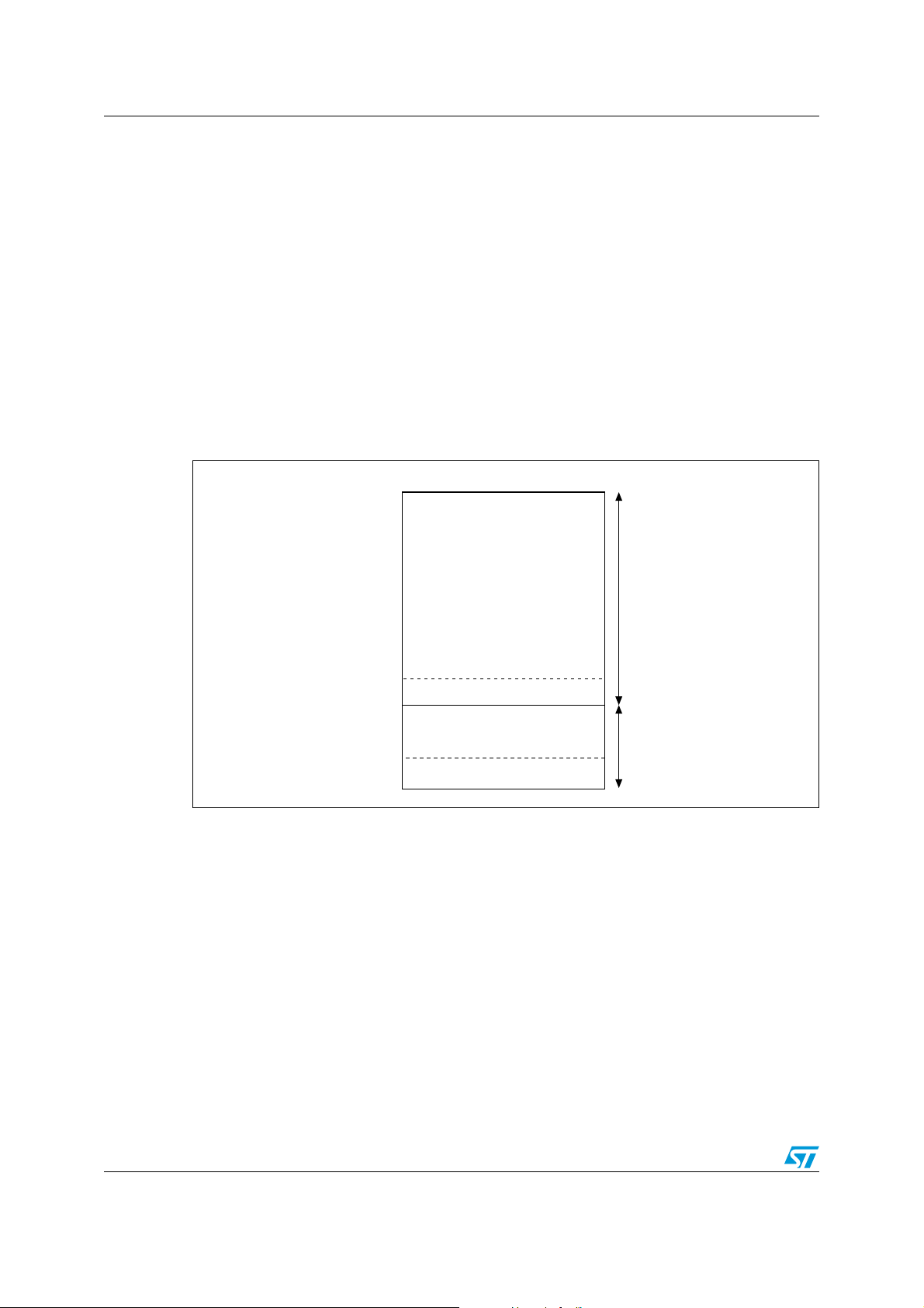
Flash memory
0x0800 0FFF
0x0800 1000
IAP code
Vector table
User code
Vector table
0x0800 0000
To p F l ash memory
address
User space
memory
IAP space
memory
ai17364
1 IAP overview
1.1 Principle
The IAP driver must be programmed from the Flash memory base address via the JTAG or
SWD interface using a development toolchain. This driver uses the I2C to load a file from
the host to the STM32F10x’s internal Flash memory, and then executes it.
1.2 User program conditions
The IAP application is loaded from the Flash memory base address (0x0800 0000) to the
0x0800 0FFF address. The user application therefore has to be loaded from the
0x0800 1000 address to the top Flash memory address.
Figure 1. Flash memory usage
6/10 Doc ID 16393 Rev 1
AN3078 IAP overview
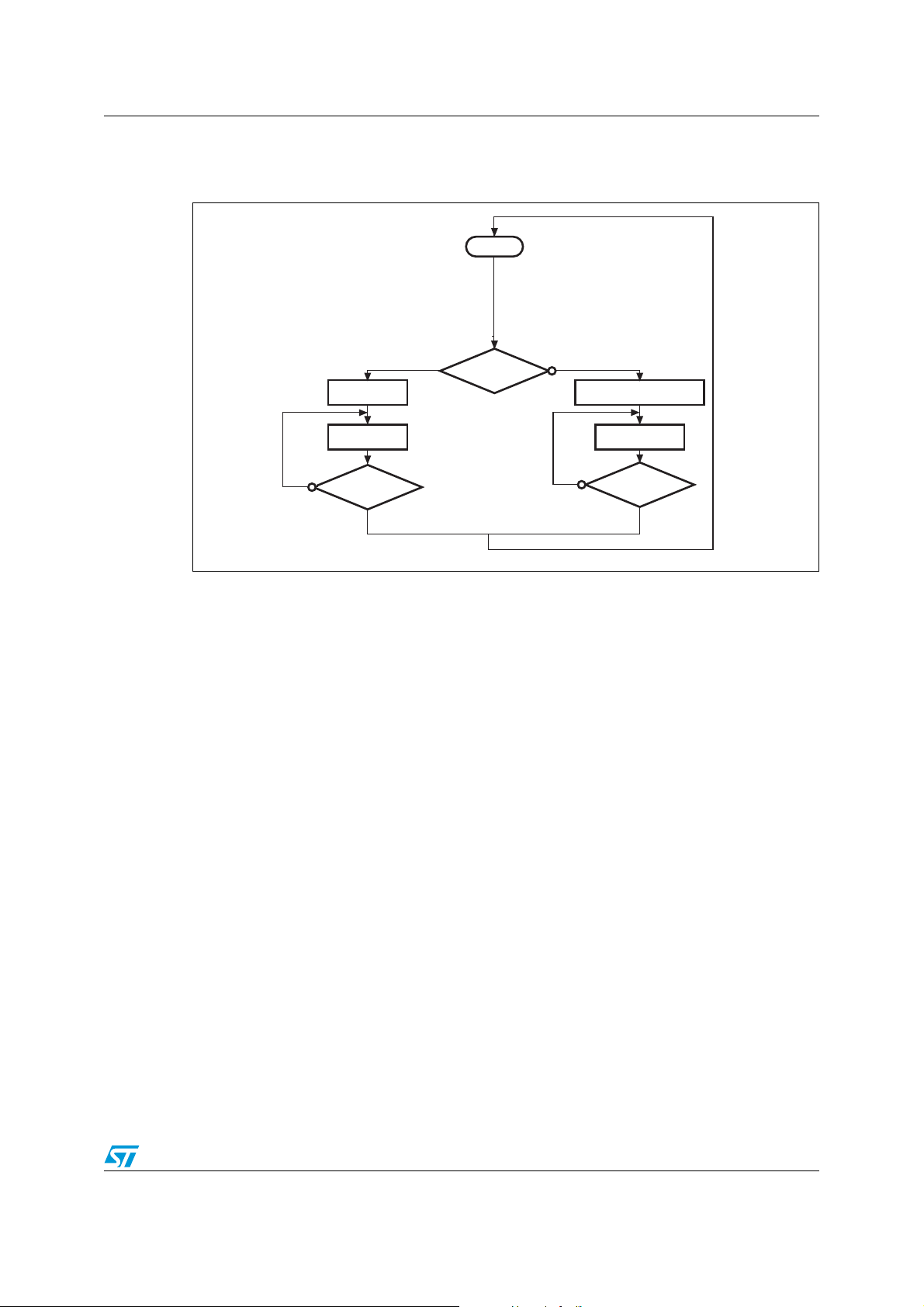
1.3 Global flowchart
Figure 2. Global flowchart
Start
Switch to IAP
IAP program
No
A pin connected to a push-button is used to select between jumping to the user application
and executing IAP for reprogramming purposes:
● at reset, when the push-button is pressed IAP is executed
● otherwise, a jump to the user program is performed
1.4 IAP commands
1.4.1 Read command
The read command is used to read data from the STM32’s Flash memory, starting from any
Flash address in the user space memory.
Reset
pressed
Yes
Yes
User button
pressed
No
Switch to User program
User program
No
Reset
pressed
Yes
ai17365
Doc ID 16393 Rev 1 7/10

IAP overview AN3078
Start
Read the Flash address
Copy from Flash to I2C1_Buffer_Tx
Send the N bytes in I2C1_Buffer_Tx
End
(expressed in 4 bytes)
Read N: number of bytes
to be read (expressed in 2 bytes)
the N bytes
via SDA line
ai17366
Figure 3. Read command flowchart
If the opcode value is OPC_READ, the Read command is performed. The target device
considers the first four bytes sent by the host master after the opcode as the Flash memory
address to be read from. The next two bytes after the Flash memory address give the size in
bytes of the data to be read. The contents of the Flash memory are buffered into
I2C1_buffer_Tx and sent by bytes via the SDA line.
1.4.2 Write command
The write command is used to write data into the STM32 Flash memory, starting from any
Flash memory address in the user space memory.
Figure 4. Write command flowchart
Start
Read the Flash address
(expressed in 4 bytes)
Read N: number of bytes
to be written (expressed in 2 bytes)
Receive the N bytes in I2C1_Buffer_Rx
Erase the needed page(s)
Program the Flash memory
End
ai17367
If the opcode value is OPC_WREN, the Write command is performed. The target device
considers the first four bytes sent by host master after the opcode as the Flash memory
address to be written to. The two next bytes after the Flash memory address give the size in
8/10 Doc ID 16393 Rev 1

AN3078 IAP overview
Erase all pages from Flash memory
base address
0x08001000 to the top Flash
memory address
Start
End
ai17369
bytes of the data to be written. The N bytes received from the host master are buffered into
RAM_BufferRx. The corresponding Flash memory page(s) is (are) erased before the data
are written.
1.4.3 Erase page command
The Erase Page command erases pages from any Flash memory base address in the user
space memory. The numbers of the pages to be erased are between 0x0001 and 0x007B (1
to 124 pages) for medium-density devices and between 0x0001 and 0x00FE (1 to 254
pages) for high-density devices.
Figure 5. Erase Page command flowchart
Start
Read the Flash memory address
(expressed in 4 bytes)
Read N: number of pages
to be erased (expressed in 2 bytes)
Erase the N pages
If the opcode value is OPC_ERPG, the Erase Page command is performed. The target
device considers the first four bytes sent by host master after the opcode as the Flash
memory address. The next two bytes after the Flash memory address give the numbers of
the pages to be erased. Once the address and page numbers have been received, the
target STM32 device erases the corresponding Flash memory pages.
1.4.4 Erase User Space memory command
The Erase User Space Memory command erases all the pages of the user space memory
from Flash memory address 0x0800 1000 to the top Flash memory address.
Figure 6. User Space Memory Erase command flowchart
End
ai17368
If the opcode value is OPC_ERUSM, the Erase User Space Memory command is
performed. As its name suggests, this command erases the contents of all pages from Flash
Doc ID 16393 Rev 1 9/10
IAP overview AN3078
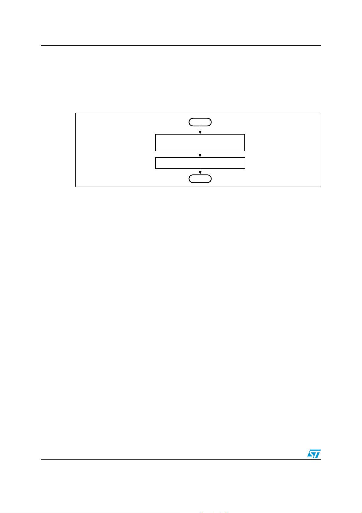
The Stack pointer is initiated
to the value of User Start Flash address
Jump to user application
Start
End
ai17370
memory base address 0x0800 1000 (the user space start address) to the top Flash memory
address.
1.4.5 Go To User Code command
The Go To User Code command allows the program to jump to the user code.
Figure 7. Go To User Code command flowchart
10/10 Doc ID 16393 Rev 1

AN3078 STM32 IAP over the I2C peripheral
STM32 device
Master Slave
Host
Program
memory
V
DD
V
SS
SDA
SCL
I2C1
R/W/E
ai17378
R
PU
R
PU
2 STM32 IAP over the I2C peripheral
This section describes how to perform IAP using the STM32 I2C peripheral.
2.1 Hardware description
Figure 15 shows a typical hardware connection between the host master and the STM32 I²C
slave target. The master and the STM32 target are connected together via the data (SDA)
and clock (SCL) pins.
A 4.7 kpull-up resistor has to be connected to both the SDA and SCL lines.
Figure 8. Hardware connection between the host master and the STM32 I
2.2 Software description
2.2.1 I2C packet description
The different packets in an I2C command are:
1. ADD_DVCE: Target address
2. R: READ BIT: the master receives the message from the target
3. W: WRITE BIT: the master will send the message to the target
4. ACK: Acknowledge
5. NACK: Not acknowledge
6. S: I2C Start condition
7. P: I2C Stop condition
8. DUM_BYTE: Dummy byte (0xFF)
2
C target
2.2.2 IAP I2C Read command
The Read command consists of two sequences:
1. I2C_write sequence: the master sends the opcode, the Flash memory address and
the number of bytes to be read.
2. I2C_read sequence: the target sends the contents of the Flash memory.
Doc ID 16393 Rev 1 11/10
STM32 IAP over the I2C peripheral AN3078
1st sequence
S ADD_DVCE W ACK O PC_RE AD ACK ADD_HGH1 AC K ADD_HGH0 ACK ADD_LOW1 ACK ADD_LOW0 ACK
NUMBR_H ACK NUMBR_L ACK P
2nd sequence
P
S ADD_DVCE
R
ACK
Data
ACK
Data
ACK
...
ACK
Data
ACK
Data
NACK
ai17379
S ADD_DVCE W ACK OPC _WR EN ACK ADD_HGH1 ACK ADD_HGH0 ACK ADD_LOW1 ACK ADD_LOW0 ACK
NUMBR_H ACK NUMBR_L ACK P
ai17380
ACK ACK ACK
DUM_BYTE Data Data
...
S ADD_DVCE W ACK O PC_ER PG ACK ADD_HGH1 ACK ADD_HGH0 ACK ADD_LOW1 ACK ADD_LOW0 ACK
NUMBR_H ACK NUMBR_L ACK P
ai17381
Figure 9. Read packet sequence using the I2C protocol
2.2.3 IAP I2C Write command
The master successively sends the slave address, the write command opcode, the Flash
memory address, the numbers of bytes to be written, a dummy byte and the bytes to be
written to the user Flash memory.
Figure 10. Write packet sequence using the I
2
C protocol
2.2.4 IAP I2C Erase Page command
The master successively sends the target address, the Erase Page command opcode, the
Flash memory address and the numbers of the pages to be erased.
Figure 11. Erase Page packet sequence using the I
2
2.2.5 IAP I2C Erase User Space Memory command
C protocol
The master successively sends the target address and the Erase User Space Memory
command opcode.
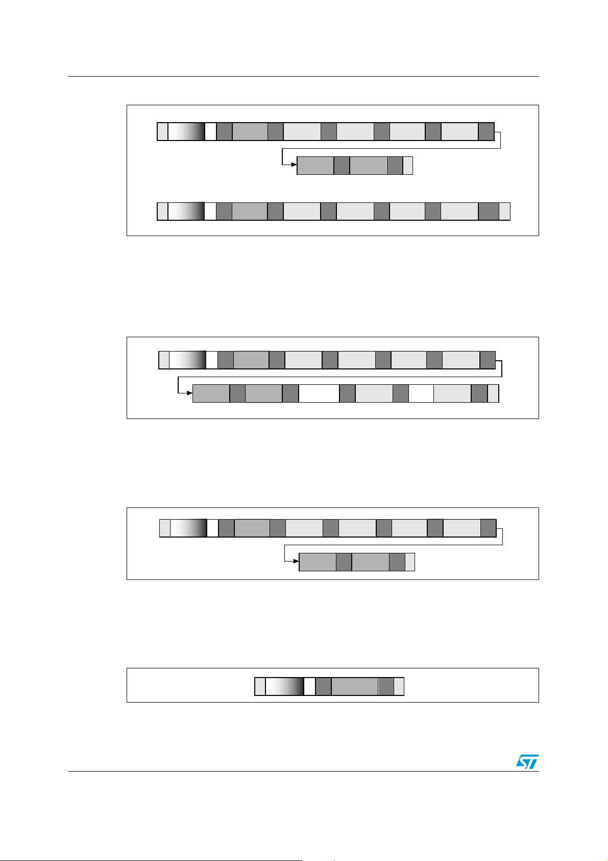
Figure 12. Erase User Space Memory packet sequence using the I
S ADD_DVCE W ACK O PC_ERU SM ACK P
12/10 Doc ID 16393 Rev 1
2
C protocol
ai17382
AN3078 STM32 IAP over the I2C peripheral
S ADD_DVCE W ACK O PC_USRCD ACK P
ai17383
2.2.6 IAP I2C Go To User Code command
The master successively sends the target address and the opcode of the Go To User Code
command.
Figure 13. Go To User Code sequence using the I
2.2.7 IAP I2C flowchart
Figure 14. IAP I2C flowchart
Start
Flash_config
NVIC_config
I2C_config
I2C_START
Yes
Read the opcode
2
C protocol
No
OPC_READ
Yes
Read command
No
OPC_WREN
Write command
Yes
No
OPC_ERPG
Yes
Erase Page
command
No
OPC_ERUSM
Erase User Space
Memory command
Yes
No
OPC_USRCD
Yes
Go to User
Application
No
ai17384
Doc ID 16393 Rev 1 13/10

Sending IAP commands to a target AN3078
3 Sending IAP commands to a target
3.1 Sending IAP I2C commands using the Aardvark I2C host adapter
3.1.1 Aardvark I2C interface mode
To use the I2C interface, select the “I2C + GPIO” or the “I2C + SPI” operational mode.
The following steps explain how to configure the Aardvark I
previous configuration.
1. Select the ‘Master’ tabsheet.
2. Set the bitrate to 100 kHz using the ‘Bitrate’ field and the ‘set’ button.
3. Set the slave address to 0x18 in the ‘Slave Addr’ field.
4. Uncheck the ‘10-Bit Addr’ option (10-bit addressing mode) because the firmware uses
the 7-bit addressing mode only.
5. Uncheck the ‘No Stop’ option.
2
C interface to match the
Figure 15. Configuration of Aardvark I
1
3
4
2
C host adapter in interface modet
2
5
Read command
The following steps explain how to read the contents of the user Flash memory:
● Step 1: Enter the byte sequence of the Read command in a Master Write message.
Refer to Section 2.2.2: IAP I2C Read command for a description of the sequence.
● Step 2: Enter the number of bytes to be read into the “Number of Bytes” field.
● Step 3: Press the ‘Master Write’ button.
● Step 4: Press the ‘Master Read’ button.
14/10 Doc ID 16393 Rev 1

AN3078 Sending IAP commands to a target
Figure 16. Read command using the Aardvark I2C interface
3
1
NUMBR_L
NUMBR_H
ADD_LOW1
ADD_HIGH1
ADD_HIGH0
Flash memory
address
ADD_LOW0
Number
of bytes
OPC_READ
2
4
ai17393
In this example, the Read command reads 16 bytes from the Flash memory address
0x0800 1000.
The figure below shows the result of the Read command transaction.
Figure 17. Read command I
2
C transaction
16 bytes read
ai17394
Write command
The following steps explain how to write to the user Flash memory:
● Step 1: Enter the byte sequence of the Write command. Refer to Section 2.2.3: IAP I2C
Write command for a description of the sequence.
● Step 2: Press the ‘Master Write’ button.
Doc ID 16393 Rev 1 15/10

Sending IAP commands to a target AN3078
OPC_WREN
1
Flash memory
address
ADD_HIGH1
ADD_HIGH0
ADD_LOW1
ADD_LOW0
NUMBR_H
NUMBR_L
Number
of bytes
DUM_BYTE
Data to be written
2
ai17395
16 bytes written
ai17396
Figure 18. Write command using the Aardvark I2C interface
In this example, the Write command writes 16 bytes to the Flash memory from address
0x0800 1000.
Figure 19 gives the result of the Write command transaction.
Figure 19. Write command I
The other IAP commands (Erase page, Erase Full User Space Memory and Go To User
Application) are issued in the same way.
3.1.2 Aardvark I2C batch mode
The Aardvark I2C host adapter is configured using the batch mode as shown in the figure
below.
Figure 20. Aardvark I
2
C configuration using the Batch mode
2
C transaction
This configuration has to be inserted into the <head> of all script I
16/10 Doc ID 16393 Rev 1
2
C commands.

AN3078 Sending IAP commands to a target
Read command
The figure below shows an example of a Read command, where 4096 bytes are read from
Flash memory address 0x0800 1000.
Figure 21. IAP I
Write command
The figure below shows an example of a Write command, where 16 bytes are written to the
Flash memory from address 0x0800 1000.
Figure 22. IAP I
2
C Read command in batch script
2
C Write command in batch script
The batch scripts of the other IAP commands (Erase Page, Erase Full User Space Memory
and Go To User Application) are written in the same way.
3.2 Sending IAP commands using another STM32 device as a bridge
3.2.1 Principle
The device firmware upgrade (DFU) project is extended to support the I2C module. The
DFU process is similar to any IAP process, so, in the case of this project, instead of
upgrading the internal Flash memory of the bridge device, the commands are transferred via
I2C peripheral to upgrade the target device.
For further information on device firmware upgrade (DFU), please refer to the dedicated
user, UM0424, available from www.st.com.
Doc ID 16393 Rev 1 17/10

Sending IAP commands to a target AN3078
System configuration DFU application
Medium access layer
I2C Flash interface layer
USB FS device library
ai17502
3.2.2 Hardware description
Figure 23 shows the hardware connection between the STM32 bridge device and the
STM32 target. The bridge is connected to the PC via USB.
Figure 23. Hardware connection between the PC, the STM32 bridge and the I
target
PC
USB
3.2.3 Firmware description
The purpose of this section is not to provide detailed information on device firmware
upgrade (for that purpose refer to user manual UM0424), but to highlight the extension and
changes made to realize the USB-I
1. DFU mode entry mechanism:
The bridge STM32F10x DFU mode is entered directly after an MCU reset.
2. DFU firmware architecture:
The Flash interface layers (internal, SPI and NOR) are omitted and a new interface
layers is added: I
The address of the I
Figure 24 shows the new DFU firmware architecture adopted for the USB-I
2
C Flash interface layer.
2
C Flash interface layer is 0x000 1000.
Bridge
STM32
2
C bridge.
V
DD
SDA
SCL SCL
V
SS
2
C
I2C target
V
R
PD
DD
STM32
SDA
V
SS
ai17501
2
C bridge.
Figure 24. Modified DFU firmware architecture
18/10 Doc ID 16393 Rev 1
AN3078 IAP timings
4 IAP timings
This section gives an idea of the time required to program a file into the STM32’s internal
Flash memory.
Table 1. IAP timings
Settings IAP via I2C
Communication protocol settings 400 kHz, 7-bit addressing mode
Download time
Download time
(bits/s) 11980
Speed
1. Download time = erase time + program time + verify time.
(1)
(508 Kbytes)
(1)
(124 Kbytes) 105 s
358 s
Doc ID 16393 Rev 1 19/10

Revision history AN3078
5 Revision history
Table 2. Document revision history
Date Revision Changes
12-Jul-2010 1 Initial release.
20/10 Doc ID 16393 Rev 1

AN3078
Please Read Carefully:
Information in this document is provided solely in connection with ST products. STMicroelectronics NV and its subsidiaries (“ST”) reserve the
right to make changes, corrections, modifications or improvements, to this document, and the products and services described herein at any
time, without notice.
All ST products are sold pursuant to ST’s terms and conditions of sale.
Purchasers are solely responsible for the choice, selection and use of the ST products and services described herein, and ST assumes no
liability whatsoever relating to the choice, selection or use of the ST products and services described herein.
No license, express or implied, by estoppel or otherwise, to any intellectual property rights is granted under this document. If any part of this
document refers to any third party products or services it shall not be deemed a license grant by ST for the use of such third party products
or services, or any intellectual property contained therein or considered as a warranty covering the use in any manner whatsoever of such
third party products or services or any intellectual property contained therein.
UNLESS OTHERWISE SET FORTH IN ST’S TERMS AND CONDITIONS OF SALE ST DISCLAIMS ANY EXPRESS OR IMPLIED
WARRANTY WITH RESPECT TO THE USE AND/OR SALE OF ST PRODUCTS INCLUDING WITHOUT LIMITATION IMPLIED
WARRANTIES OF MERCHANTABILITY, FITNESS FOR A PARTICULAR PURPOSE (AND THEIR EQUIVALENTS UNDER THE LAWS
OF ANY JURISDICTION), OR INFRINGEMENT OF ANY PATENT, COPYRIGHT OR OTHER INTELLECTUAL PROPERTY RIGHT.
UNLESS EXPRESSLY APPROVED IN WRITING BY AN AUTHORIZED ST REPRESENTATIVE, ST PRODUCTS ARE NOT
RECOMMENDED, AUTHORIZED OR WARRANTED FOR USE IN MILITARY, AIR CRAFT, SPACE, LIFE SAVING, OR LIFE SUSTAINING
APPLICATIONS, NOR IN PRODUCTS OR SYSTEMS WHERE FAILURE OR MALFUNCTION MAY RESULT IN PERSONAL INJURY,
DEATH, OR SEVERE PROPERTY OR ENVIRONMENTAL DAMAGE. ST PRODUCTS WHICH ARE NOT SPECIFIED AS "AUTOMOTIVE
GRADE" MAY ONLY BE USED IN AUTOMOTIVE APPLICATIONS AT USER’S OWN RISK.
Resale of ST products with provisions different from the statements and/or technical features set forth in this document shall immediately void
any warranty granted by ST for the ST product or service described herein and shall not create or extend in any manner whatsoever, any
liability of ST.
ST and the ST logo are trademarks or registered trademarks of ST in various countries.
Information in this document supersedes and replaces all information previously supplied.
The ST logo is a registered trademark of STMicroelectronics. All other names are the property of their respective owners.
© 2010 STMicroelectronics - All rights reserved
STMicroelectronics group of companies
Australia - Belgium - Brazil - Canada - China - Czech Republic - Finland - France - Germany - Hong Kong - India - Israel - Italy - Japan -
Malaysia - Malta - Morocco - Philippines - Singapore - Spain - Sweden - Switzerland - United Kingdom - United States of America
www.st.com
Doc ID 16393 Rev 1 21/21
 Loading...