

Page 1

AN3064
Application note
Using the STC3100 battery monitor for gas gauge applications
Introduction
Handheld devices such as mobile phones, music and video players, as well as portable
navigation devices, tend to integrate ever more multimedia functions, all of which have
different power needs. As a consequence, it has become difficult to manage the battery’s
state-of-charge (SoC) and predict the remaining operating time with no dedicated gas
gauge support. The STC3100 is a new device that includes battery monitoring features
(voltage, current and temperature) and a Coulomb counter to implement a gas gauge
system in existing or future applications.
This application note is intended to assist product designers by taking advantage of using
the STC3100 in one-cell Li-Ion battery handheld applications to implement the gas gauge
function. The document provides:
■ a brief description of the STC3100 device and typical applications,
■ information on how to use the battery monitoring functions of the STC3100,
■ a general flow chart of the tasks needed to implement a simple gas gauge system.
October 2009 Doc ID 16263 Rev 1 1/15
www.st.com
Page 2
Using the STC3100 AN3064
1 Using the STC3100
1.1 Brief description of the STC3100
The STC3100 battery monitoring function includes the measurement of the battery voltage
and current, measurement of the IC’s die temperature and computation of the battery
charge variation (Coulomb counter). An external sense resistor is used in series with the
battery to adapt the current measurement to the application requirements.
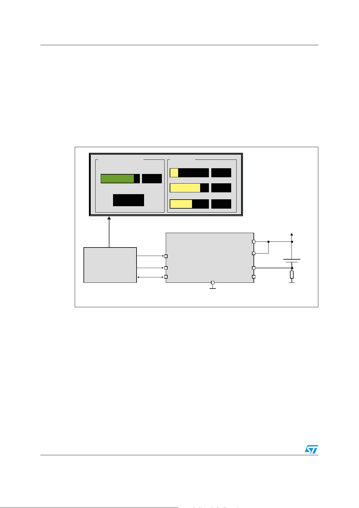
Figure 1 shows a typical application using the STC3100.
Figure 1. Typical application diagram for the STC3100
Battery State-of-charge
Remaining percentage
Remaining time
2:06
uC with
Gas Gauge
firmware
80 %
32768 Hz
clock
I2C bus
Battery data
Current
Voltage
Temperature
ROSC
SCL
SDA
0.32 A
3.71 V
STC3100
GND
27 ° C
VCC
VIN
CG
IO0
Battery
Rcg
AM04578
The STC3100 mode and operation are controlled through an I²C interface. SCL and SDA
are the clock and data signals of the I²C interface.
1.2 Internal or external 32,768 Hz timebase
The Coulomb counter system needs an accurate 32,768 Hz timebase to compute the level
of charge flowing from and to the battery. The STC3100 can operate from an internal
oscillator or use an external RTC signal for highest accuracy. To use the internal oscillator, a
200 kΩ 0.1% resistor must be connected to the ROSC pin. The accuracy of the internal
oscillator is 2.5% maximum over the supply voltage and temperature ranges. An external
RTC signal can be applied to the ROSC pin (no resistor required in this case). The signal
must be a square wave with a low level below 0.5 V and a high level above 1.5 V.
2/15 Doc ID 16263 Rev 1
Page 3
AN3064 Using the STC3100
Figure 2. ROSC connection for internal or external timebase
200 kΩ, 0.1%
ROSC
STC3100
The STC3100 automatically recognizes the presence of the external clock signal and uses it
if present. The internal oscillator, however, can be inhibited to force the use of an external
signal by setting the SEL_EXT_CLK bit in the REG_MODE register.
1.3 STC3100 external components
The Rcg resistor is used to sense the current flowing into or from the battery. The value of
the Rcg resistor must be selected based on the maximum peak current in the application;
the voltage drop across the Rcg resistor must not exceed +/-80 mV.
Rcg resistance (Ohm) <= 0.08/peak current (A).
For instance, a current of up to +/- 2 A can be monitored using a 33 mΩ resistor.
The STC3100 has separate pins for the power supply (VCC) and voltage measurement
(VIN) inputs, providing an easy way of implementing an input filter or additional ESD
protection without affecting the accuracy of the voltage measurement.
32,768 Hz RTC
ROSC
STC3100
AM04579
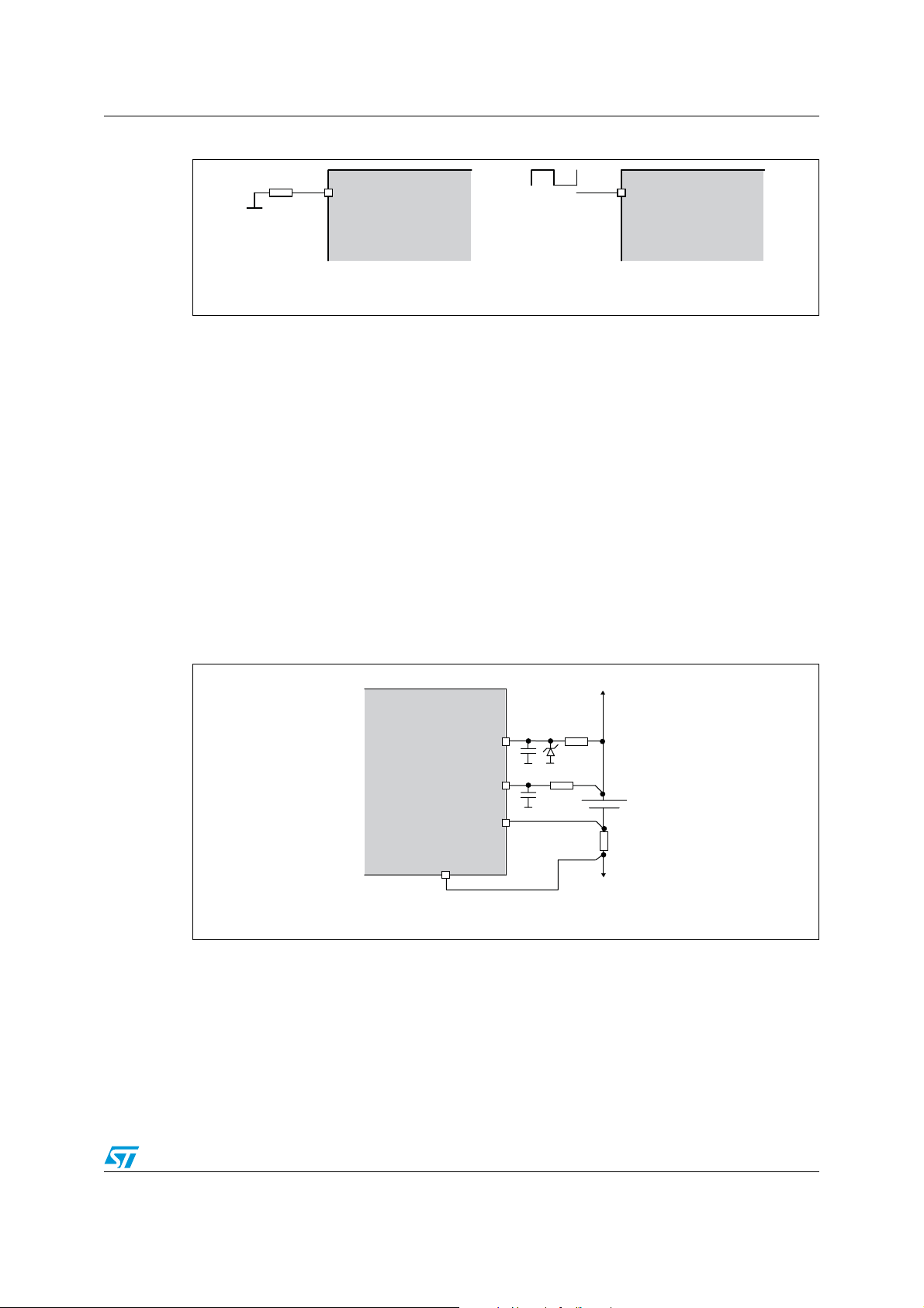
Figure 3. STC3100 connections with VIN input filter and additional ESD protection
System supply
R1
R2
Battery
Rcg
Gnd
AM04580
STC3100
GND
VCC
VIN
CG
C1C2D1
C1 is the normal recommended decoupling capacitor (1 µF).
R1 and D1 provide additional ESD protection to the STC3100’s VCC pin. A typical value for
R1 is 150 Ω and D1 is a 5.6 V Zener diode.
R2 provides additional ESD protection to the STC3100’s VIN pin. A typical value for R2 is
1 kΩ.. The input impedance of the VIN pin is approximately 500 kΩ; an R2 resistor value of
1 kΩ will not affect the accuracy of the battery voltage measurement. The VIN input must be
connected directly (through the R2 resistor) to the battery’s positive terminal.
Doc ID 16263 Rev 1 3/15
Page 4

Using the STC3100 AN3064
The C2 capacitor is optional and can be used if additional filtering is required, with typical
values of 47 to 220 nF.
The STC3100’s ground connection (GND) is used as the reference input for the current
measurement and must be connected to the ground side of the sense resistor by a
dedicated track. No current, except the supply current of the STC3100 itself, must flow in
this track to avoid creating an offset error in the current measurement.
4/15 Doc ID 16263 Rev 1
Page 5

AN3064 Battery monitoring functions
2 Battery monitoring functions
The STC3100 includes the following battery monitoring functions.
● A Coulomb counter for automatic computation of the battery’s charge variation: this is
done by integrating the battery current versus the time and accumulating the resulting
charge variation into the accumulator register. The last current measurement is always
available.
● Automatic periodic measurement of the battery voltage.
● Automatic periodic measurement of the temperature using the STC3100’s internal
sensor.
The battery monitoring functions are controlled by the GG_RUN bit in the REG_MODE
register. Since GG_RUN is reset at power-up, the battery monitoring functions are disabled,
ensuring a low standby current when the battery is inserted until the application is started.
The Coulomb counter function uses a 12/14-bit ADC and runs continuously after it has been
enabled by the GG_RUN bit.
Values held in consecutive registers (such as the charge value in the REG_CHARGE_LOW
and REG_CHARGE_HIGH registers) must be read with a single I
integrity. Multiple values can be read in one I²C access; all values will then be consistent,
that is, will be relative to the same time.
2.1 Coulomb counter operation
The voltage drop between the CG and GND pins is integrated during a conversion period
and input to a 12- to 14-bit AD converter. The output conversion is accumulated into a 28-bit
accumulator. The system controller can control the Coulomb counter and read the data
(upper 16 bits of the accumulator) through the I
2
C control registers.
2
C access to ensure data
Doc ID 16263 Rev 1 5/15
Page 6

Battery monitoring functions AN3064
Figure 4. Gas gauge block diagram
Control
registers
16
16
16
rd_req
Counter
register
Current
register
Charge
register
AM00832
CG
GND
12/14-bit
AD converter
EOC
2
cg_res
cg_clock
cg_enable
cg_calibration
16-bit counter
28
28-bit
accumulator
16
32768 Hz
Σ
28
cg_rst
Control logic
The A/D converter’s output is a signed value in two’s complement format. It is positive when
the battery is charging and negative when the battery is discharging. When a conversion
cycle is completed, the result is added to the charge accumulator and the 16-bit conversion
counter is incremented.
6/15 Doc ID 16263 Rev 1
Page 7

AN3064 Battery monitoring functions
Figure 5. Coulomb counter operation
I
battery
current
(mA)
Δt
Acc
Coulomb
counter
accumulator
(mA.h)
Idle Fast charge End of
Coulomb counter detail:
current samples are
accumulated at each
end of conversion:
Acc = Σ(Ι x Δt)
charge
2.2 Coulomb counter reading
The charge data as well as the conversion count can be read at any time by the system
controller. The recommended procedure is to read the locations REG_CHARGE (2 bytes)
and REG_COUNTER (2 bytes) in one go using a single I²C block read to ensure data
consistency between the accumulator and counter.
Table 1. REG_CHARGE_LOW. address 2 (02h)
Idle Medium
discharge rate
Fast
discharge rate
Charge
current
Time
Discharge
current
Time
End of
discharge
AM04581
Name Pos. Type
Power-
up
Description
DATA[7..0] [7..0] R 00 Coulomb counter data
Table 2. REG_CHARGE_HIGH. address 3 (03h)
Name Pos. Type
Power-
up
Description
DATA[15..8] [7..0] R 00 Coulomb counter data
The charge code is a 16-bit binary number using the two’s complement binary format. Bit 15
is the sign bit and the LSB value is 6.70 µV.h. To convert the charge data into mA.h, the
external resistance Rsense must be taken into account:
charge data (mA.h) = 6.70 * charge_code / Rsense (mΩ).
When the result of an accumulation exceeds the limits of a signed binary number (below
0x8000 or above 0x7FFFF), the carry bit is lost, no overflow is generated and the
accumulator continues to accumulate.
Doc ID 16263 Rev 1 7/15
Page 8

Battery monitoring functions AN3064
Table 3. REG_COUNTER_LOW. address 4 (04h)
Name Pos. Type
DATA[7..0] [7..0] R 00 Conversion counter data.
Table 4. REG_COUNTER_HIGH. address 5 (05h)
Name Pos. Type Power-up Description
DATA[15..8] [7..0] R 00 Conversion counter data
The counter code is an unsigned 16-bit binary number.
When the conversion counter reaches its maximum value (binary code = 2
wraps to 0 and continues counting. Both the accumulator and the counter can be reset with
the GG_RST bit.
The CG_EOC bit in the REG_CTRL register can be used to check that at least one new
current measurement has been done and accumulated since the last reading of the
REG_CTRL register.
2.3 Battery current reading
The last measured value of the current is available in the REG_CURRENT locations (two
bytes) and is updated at each conversion.
Table 5. REG_CURRENT_LOW. address 6 (06h)
Power-
up
Description
16
-1 = 0xFFFF), it
Name Pos. Type Power-up Description
DATA[7..0] [7..0] R 00 Battery current data
Table 6. REG_CURRENT_HIGH. address 7 (07h)
Name Pos. Type Power-up Description
DATA[13..8] [5..0] R 00 Battery current data
DATA[15, 14] [7,6] R 0 Unused
The current code is a 14-bit binary number using the two’s complement binary format. Bit 13
is the sign bit and bits 0 to 12 are the data bits. The LSB value (bit 0) is 11.77 µV.h,
irrespective of the current conversion resolution. However, bit 0 is always zero in 12- and 13bit resolution modes, and bit 1 is always zero in 12-bit resolution mode. To convert the
current data into mA, the external resistance Rsense must be taken into account.
current (mA) = current_code* 11.77 / Rsense (mΩ)
8/15 Doc ID 16263 Rev 1
Page 9

AN3064 Battery monitoring functions
2.4 Battery voltage and temperature reading
The battery voltage and chip temperature (close to the battery temperature) are measured
by means of an A/D converter and a multiplexer. This function takes place concurrently to
the Coulomb counter function with a dedicated A/D converter, which means that it does not
affect the performance of the Coulomb counter. To reduce the power consumption, a
conversion takes place every two seconds only, alternating between the battery voltage and
temperature (so each value is refreshed every four seconds).
Table 7. REG_VOLTAGE_LOW. address 8 (08h)
Name Pos. Type Power-up Description
DATA[7..0] [7..0] R 00 Battery voltage data
Table 8. REG_VOLTAGE_HIGH. address 9 (09h)
Name Pos. Type Power-up Description
DATA[11..8] [3..0] R 0 Battery voltage data
DATA[15..12] [7..4] R 0 unused
The voltage code is a 12-bit binary number using the two’s complement binary format. Bit 11
is the sign bit and bits 0 to 10 are the data bits. The LSB value (bit 0) is 2.44 mV. Note that
although the input voltage range is limited to a positive voltage, negative voltage codes can
be read when the input voltage is close to 0 V due to internal offset effects.
Table 9. REG_TEMPERATURE_LOW. address 10 (0Ah)
Name Pos. Type Power-up Description
DATA[7..0] [7..0] R 00 Temperature data
Table 10. REG_TEMPERATURE_HIGH. address 11 (0Bh)
Name Pos. Type Power-up Description
DATA[11..8] [3..0] R 0 Temperature data
DATA[15..12] [7..4] R 0 unused
The temperature code is a 12-bit binary number using the two’s complement binary format.
Bit 11 is the sign bit and bits 0 to 10 are the data bits. The LSB value (bit 0) is 0.125° C.
The actual values of the voltage and temperature are:
● voltage (mV) = Voltage_code * 2.44.
● temperature (°C) = Temperature_code * 0.125.
The VTM_EOC bit in the REG_CTRL register can be used to check that at least one new
measurement of the voltage or temperature has been done since the last reading of the
REG_CTRL register.
Doc ID 16263 Rev 1 9/15
Page 10

Controller tasks for gas gauge implementation AN3064
3 Controller tasks for gas gauge implementation
The system controller manages the following tasks.
● At start-up, it enables the STC3100’s battery monitoring functions.
● It periodically reads the battery voltage, temperature, current and charge accumulator
and uses this information to estimate the state of charge.
● At power-down, it disables the STC3100.
Figure 6. Flow chart of the general gas gauge system
Application startup
Enable the STC3100
Set-up a periodic task ‘GasGauge’
Periodic task ‘GasGauge’
Application shutdown
3.1 Application start-up
A typical startup code writes 0x02 (hex value) into the REG_CTRL register to reset the
accumulator and counter and clear the PORDET bit, and then 0x10 into the REG_MODE
register to start the STC3100 in 14-bit resolution mode.
The startup code then sets a periodic GasGauge task that will be called every 5 seconds.
3.2 Periodic GasGauge task
A simple periodic GasGauge task will do the following.
● Read the battery voltage, temperature, current and charge accumulator.
● At first call, use the battery voltage to estimate the battery’s state-of-charge and save it
in a RAM location of the STC3100 as a reference value.
● During subsequent calls, use the saved reference value and the present charge
register content to calculate the present battery capacity:
battery capacity = reference value + charge register content.
● Trigger a "low battery" alarm if the battery’s voltage is low (typically less than 3.1 V).
● Calculate the remaining operating time from the remaining battery capacity and current
consumption when the battery is not charging (negative current).
Read the STC3100 data
Process the gas gauge system
Disable the STC3100
AM04582
3.3 Application power-down
The shutdown code puts the STC3100 in standby mode by writing 0 into the REG_MODE
register.
10/15 Doc ID 16263 Rev 1
Page 11

AN3064 STC3100 demonstration board
Appendix A STC3100 demonstration board
The STC3100 demonstration board is convenient to evaluate the charge and battery
monitoring functions and quickly obtain a working prototype or design reference.
Figure 7 shows the basic connections to use the STC3100 demonstration board.
Figure 7. STC3100 demonstration board usage
System
controller
Gnd
(optional)
32768 Hz
SDA
SCL
| Battery +
AM04583
The sense resistor is on the board and the resistance value is 33 mΩ.
The digital interface comprises the SDA and SCL pads (I
2
C bus signals). An external
32,768 Hz clock can be applied to the ROSC pad. It is not necessary to physically remove
the ROSC resistor. The digital levels are: <0.5 V for low level, >1.5 V for high level.
Doc ID 16263 Rev 1 11/15
Page 12

STC3100 register map AN3064
Appendix B STC3100 register map
Ta bl e 1 1 details the mapping of the battery monitoring registers.
Table 11. Register map
Name
Control registers
REG_MODE 0 R/W Mode register
REG_CTRL 1 R/W Control and status register
REG_CHARGE_LOW 2 R Coulomb counter data, bits 0-7
REG_CHARGE_HIGH 3 R Coulomb counter data, bits 8-15
REG_COUNTER_LOW 4 R Conversion counter, bits 0-7
REG_COUNTER_HIGH 5 R Conversion counter, bits 8-15
REG_CURRENT_LOW 6 R Battery current value, bits 0-7
REG_CURRENT_HIGH 7 R Battery current value, bits 8-15
REG_VOLTAGE_LOW 8 R Battery voltage value, bits 0-7
REG_VOLTAGE_HIGH 9 R Battery voltage value, bits 8-15
REG_TEMPERATURE_LOW 10 R Temperature value, bits 0-7
REG_TEMPERATURE_HIGH 11 R Temperature value, bits 8-15
Device ID registers
REG_ID0 24 R Part type ID = 10h
REG_ID1 25 R Unique part ID, bits 0-7
REG_ID2 26 R Unique part ID, bits 8-15
REG_ID3 27 R Unique part ID, bits 16-23
Address
(dec.)
Type Description
REG_ID4 28 R Unique part ID, bits 24-31
REG_ID5 29 R Unique part ID, bits 32-39
REG_ID6 30 R Unique part ID, bits 40-47
REG_ID7 31 R Device ID CRC
RAM registers
REG_RAM0 32 R/W General-purpose RAM register 0
... ... ...
REG_RAM31 63 R/W General-purpose RAM register 31
The REG_MODE and REG_CTRL registers are described in detail in Ta b le 1 2 and
Ta bl e 1 3.
12/15 Doc ID 16263 Rev 1
Page 13

AN3064 STC3100 register map
Table 12. REG_MODE. address 0 (00h)
Name Pos. Type
Power-
up
SEL_EXT_CLK 0 R/W 0
GG_RES [2,1] R/W 00
GG_CAL 3 R/W 0
GG_RUN 4 R/W 0
[7..5] Unused
Table 13. REG_CTRL. address 1 (01h)
Name Pos. Type
Power-
up
RX
IO0DATA 0
W1
Description
32,768 Hz clock source:
0: auto-detect, 1: external clock
Current/Coulomb counter ADC resolution:
00: 14 bits, 01: 13 bits, 10: 12 bits
0: no effect
1: used to calibrate the AD converters
0: standby mode. Accumulator and counter
registers are frozen, battery monitoring functions
are in standby.
1: operating mode
Description
Port IO0 data status:
0 = IO0 input is low, 1 = IO0 input is high
Port IO0 data output drive:
0 = IO0 output is driven low,1 = IO0 output is open
GG_RST 1 W 0
GG_EOC 2 R 1
VTM_EOC 3 R 1
R1
PORDET 4
W0
[7..5] R/W Unused
0: no effect
1: resets the charge accumulator and conversion
counter. GG_RST is a self-clearing bit.
Set at the end of a battery current conversion
cycle. Clears upon reading.
Set at the end of a battery voltage or temperature
conversion cycle. Clears upon reading.
Power-on reset (POR) detection bit:
0 = no POR event occurred
1 = POR event occurred
Soft reset:
0 = releases the soft-reset and clears the POR
detection bit
1 = asserts the soft-reset and sets the POR
detection bit
Doc ID 16263 Rev 1 13/15
Page 14

References AN3064
References
Table 14. Document references
Document
STC3100 datasheet: Battery monitor IC with Coulomb counter/gas gauge.
Revision history
Table 15. Document revision history
Date Revision Changes
19-Oct-2009 1 Initial release.
14/15 Doc ID 16263 Rev 1
Page 15

AN3064
Please Read Carefully:
Information in this document is provided solely in connection with ST products. STMicroelectronics NV and its subsidiaries (“ST”) reserve the
right to make changes, corrections, modifications or improvements, to this document, and the products and services described herein at any
time, without notice.
All ST products are sold pursuant to ST’s terms and conditions of sale.
Purchasers are solely responsible for the choice, selection and use of the ST products and services described herein, and ST assumes no
liability whatsoever relating to the choice, selection or use of the ST products and services described herein.
No license, express or implied, by estoppel or otherwise, to any intellectual property rights is granted under this document. If any part of this
document refers to any third party products or services it shall not be deemed a license grant by ST for the use of such third party products
or services, or any intellectual property contained therein or considered as a warranty covering the use in any manner whatsoever of such
third party products or services or any intellectual property contained therein.
UNLESS OTHERWISE SET FORTH IN ST’S TERMS AND CONDITIONS OF SALE ST DISCLAIMS ANY EXPRESS OR IMPLIED
WARRANTY WITH RESPECT TO THE USE AND/OR SALE OF ST PRODUCTS INCLUDING WITHOUT LIMITATION IMPLIED
WARRANTIES OF MERCHANTABILITY, FITNESS FOR A PARTICULAR PURPOSE (AND THEIR EQUIVALENTS UNDER THE LAWS
OF ANY JURISDICTION), OR INFRINGEMENT OF ANY PATENT, COPYRIGHT OR OTHER INTELLECTUAL PROPERTY RIGHT.
UNLESS EXPRESSLY APPROVED IN WRITING BY AN AUTHORIZED ST REPRESENTATIVE, ST PRODUCTS ARE NOT
RECOMMENDED, AUTHORIZED OR WARRANTED FOR USE IN MILITARY, AIR CRAFT, SPACE, LIFE SAVING, OR LIFE SUSTAINING
APPLICATIONS, NOR IN PRODUCTS OR SYSTEMS WHERE FAILURE OR MALFUNCTION MAY RESULT IN PERSONAL INJURY,
DEATH, OR SEVERE PROPERTY OR ENVIRONMENTAL DAMAGE. ST PRODUCTS WHICH ARE NOT SPECIFIED AS "AUTOMOTIVE
GRADE" MAY ONLY BE USED IN AUTOMOTIVE APPLICATIONS AT USER’S OWN RISK.
Resale of ST products with provisions different from the statements and/or technical features set forth in this document shall immediately void
any warranty granted by ST for the ST product or service described herein and shall not create or extend in any manner whatsoever, any
liability of ST.
ST and the ST logo are trademarks or registered trademarks of ST in various countries.
Information in this document supersedes and replaces all information previously supplied.
The ST logo is a registered trademark of STMicroelectronics. All other names are the property of their respective owners.
© 2009 STMicroelectronics - All rights reserved
STMicroelectronics group of companies
Australia - Belgium - Brazil - Canada - China - Czech Republic - Finland - France - Germany - Hong Kong - India - Israel - Italy - Japan -
Malaysia - Malta - Morocco - Philippines - Singapore - Spain - Sweden - Switzerland - United Kingdom - United States of America
www.st.com
Doc ID 16263 Rev 1 15/15
 Loading...