How it Works
Log In / Sign Up
Buy Points
How it Works
FAQ
Contact Us
Questions and Suggestions
Users
Datasheet
Loading...
A
AN291
AN292
AN2927
AN2928
AN2929
AN293
AN2931
AN2933
AN2936
AN2937
AN2938
AN2941
AN2944
AN2945
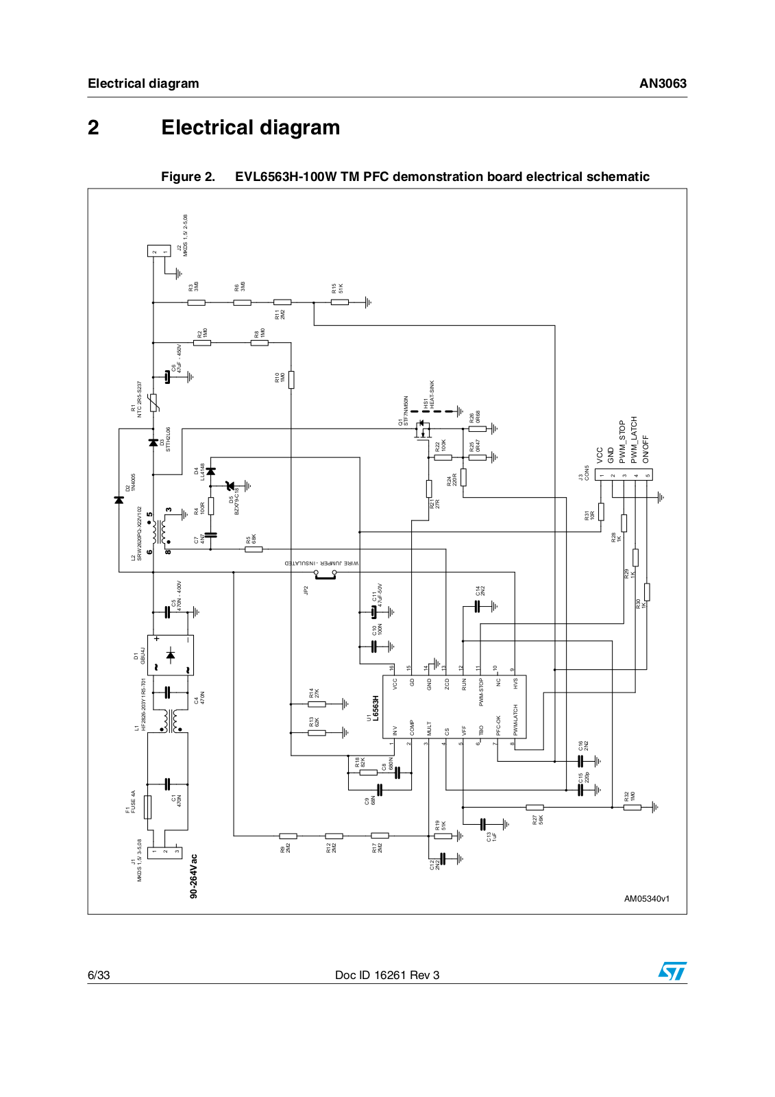
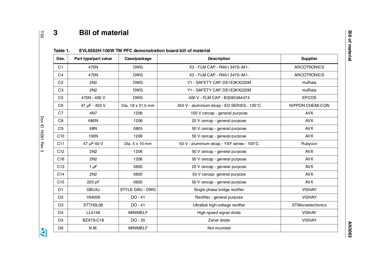
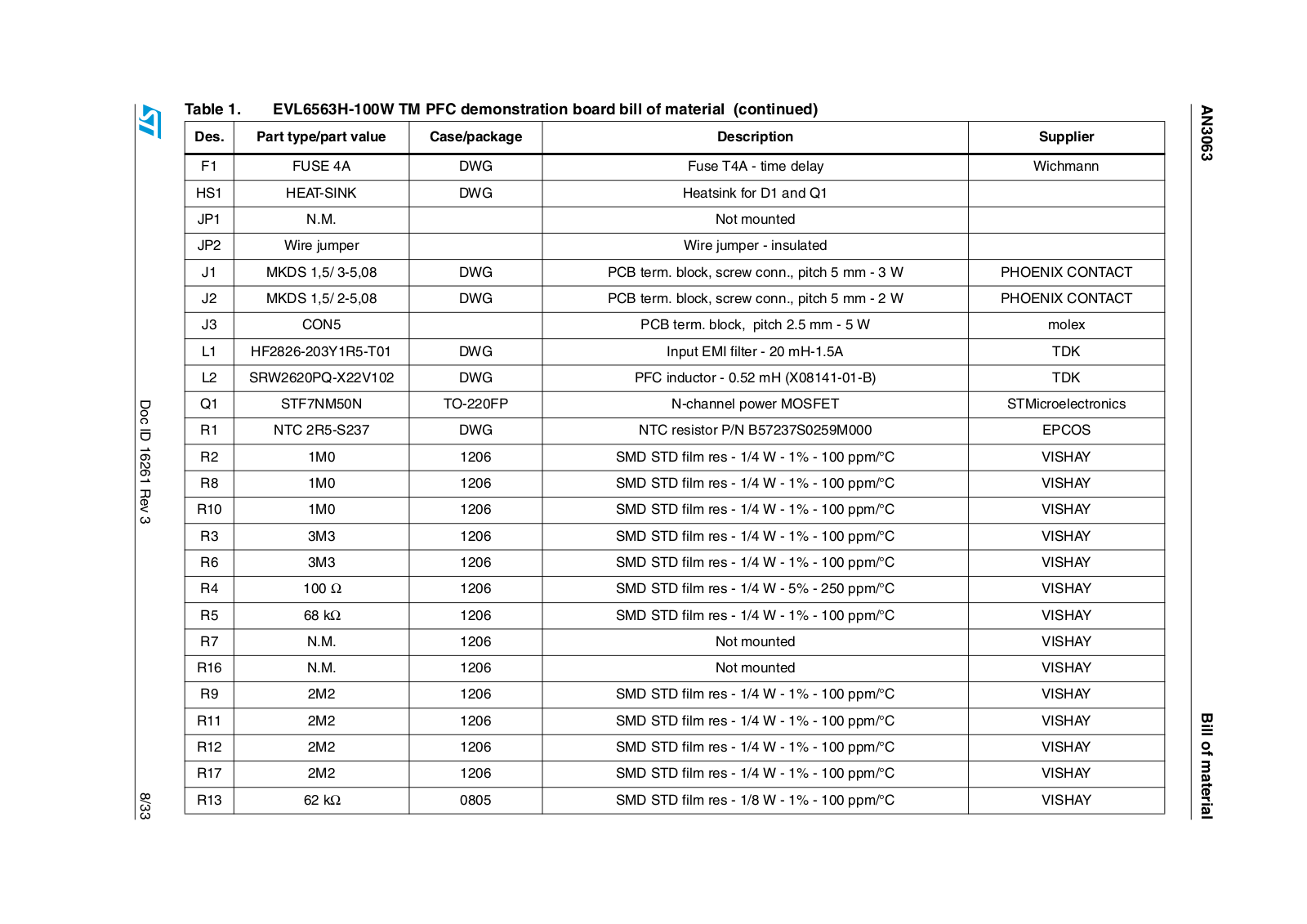
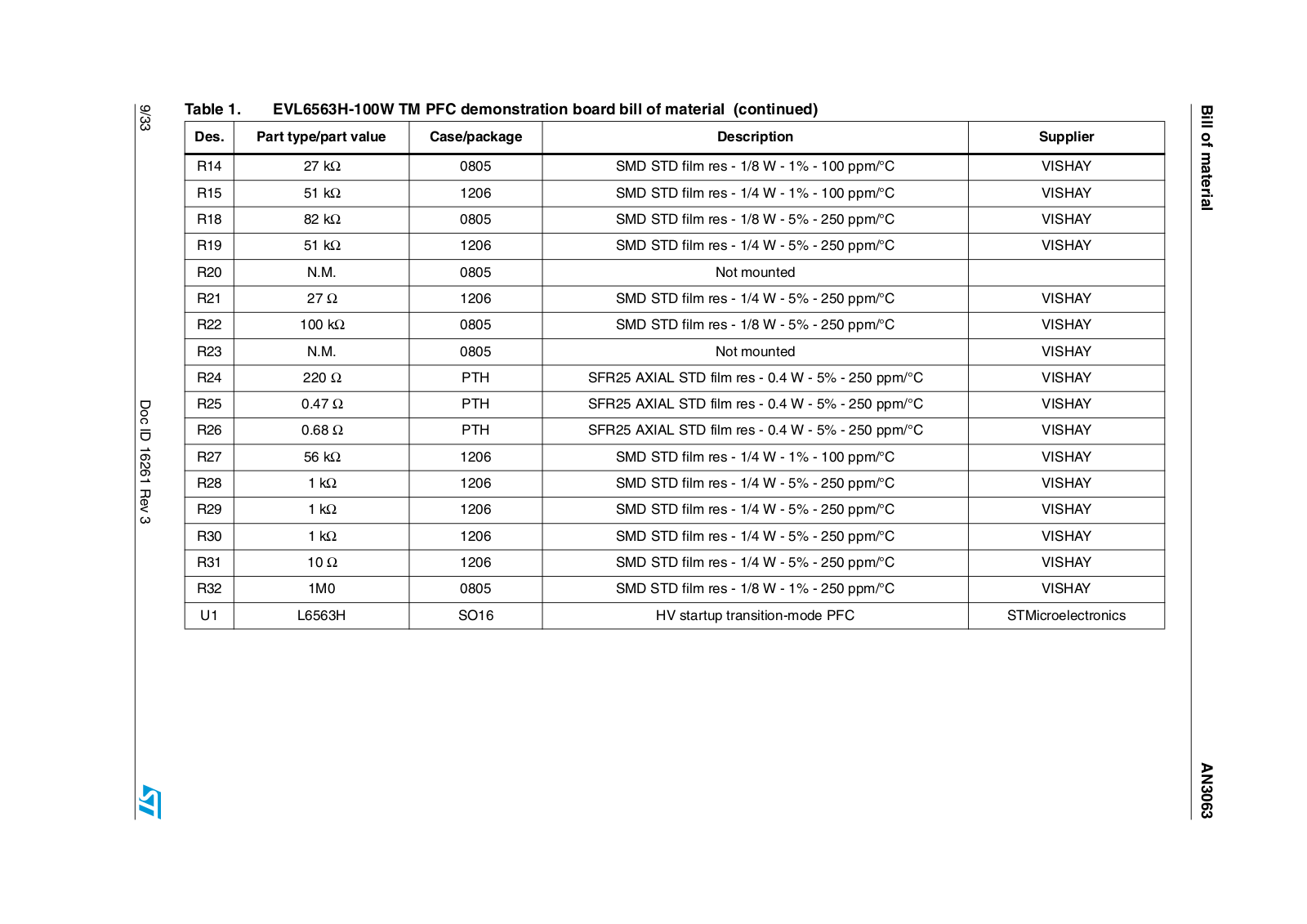
2
AN2946
AN2950
AN2951
AN2952
AN2953
AN2960
AN2961
AN2966
AN2967
AN2970
AN2979
AN2983
AN2984
AN2985
AN2986
AN2989
AN299
AN2994
AN2995
AN3000
AN3001
AN3008
AN3011
AN3012
AN3018
AN3023
AN3024
AN3027
AN3029
AN303
AN3032
AN3040
AN3046
AN3050
AN306
AN3060
AN3063
AN3064
AN3065
AN307
AN3070
AN3075
AN3078
AN308
2
AN3089
AN3090
AN3093
AN3094
AN3095
AN3097
AN3099
AN310
AN3100
AN3101
AN3102
AN3103
AN3105
AN3106
AN3107
AN3108
AN3109
AN311
AN3110
AN3111
AN3112
AN3114
AN3115
AN3116
AN3117S
AN3117SA
AN3118
AN3119
AN3123
AN3127
AN3128
AN3129
AN3133
AN3134
AN3137
AN3138
AN3139
AN3140
AN3141
AN3142
AN3143
AN3144
Loading...
Loading...
Nothing found
AN3063
APPLICATION NOTE (ST)
33 pgs
1.53 Mb
0
Table of contents
Loading...
Datasheet AN3063 APPLICATION NOTE (ST)
...
Datasheet APPLICATION NOTE (ST)
Download
Specifications and Main Features
Frequently Asked Questions
User Manual
Download
Page 1
Page 2
Page 3
Page 4
Page 5
Page 6
Page 7
Page 8
Page 9
Page 10
Page 11
Page 12
Page 13
Page 14
Page 15
Page 16
Page 17
Page 18
Page 19
Page 20
Page 21
Page 22
Page 23
Page 24
Page 25
Page 26
Page 27
Page 28
Page 29
Page 30
Page 31
Page 32
Page 33
Loading...
+
hidden pages
Unhide
You need points to download manuals.
1 point = 1 manual.
You can buy points or you can get point for every manual you upload.
Buy points
Upload your manuals


")