

Page 1

1 Introduction
In order to reduce the power consumption, size and cost of electronic devices, most
semiconductor components are manufactured using a “low voltage” process resulting in
a maximum operating voltage of 7 V or even less. Any overvoltage causes an excessive
power dissipation on the chip quickly leading to damage, or even electrical breakdown.
Portable electronic devices, such as cell phones, PDAs, MP3 players, digital cameras, etc.
are normally powered from a Li-Ion or Li-Pol battery pack, which is recharged by an internal
charger controller supplied by an external AC adapter, USB hub, etc. The failure of this
adapter or accidental usage of another adapter with a higher voltage can damage the
charger controller and lead to overvoltage on the battery, which may be very dangerous for
the device and potentially even for the user.
To avoid this, some type of protective device is absolutely necessary.
One well known solution is a device known as a Transil™. It can be understood as a Zener
diode, capable of withstanding high power dissipation. Although Transils are easy to use and
relatively inexpensive, their threshold voltage is not very accurate and is dependent upon
the current flowing through the Transil. For heavy overload, the voltage on the Transil can
still be too large and, in addition, the high power dissipation can lead to high junction
temperature, and in extreme cases the Transil and surrounding circuit board can be
damaged. For this reason, there is often a fuse connected between the supply connector
and Transil to break the circuit in case of extreme overload.
AN3050
Application note
STBP120
overvoltage protection device
Other, modern and safe devices, are integrated circuits known as “Overvoltage Protection”
(OVP) devices. The OVP device can be understood as a “firewall” between the application
and the external world represented by the power supply (AC adapter, USB, etc.), allowing
only the correct voltage to reach the application and preventing malfunction or damage
resulting from the use of an illegal or broken power supply. It contains a voltage comparator
and either a driver for external Power MOSFET, or even the Power MOSFET itself. In the
event of overvoltage, the comparator turns off the MOSFET, disconnecting the application
from the power supply. No excessive power dissipation is generated during overvoltage.
The first member of the STMicroelectronics™ OVP devices family is the STBP120, which
will be described in this application note.
November 2009 Doc ID 16207 Rev 1 1/18
www.st.com
Page 2

Contents AN3050
Contents
1 Introduction . . . . . . . . . . . . . . . . . . . . . . . . . . . . . . . . . . . . . . . . . . . . . . . . 1
2 Description . . . . . . . . . . . . . . . . . . . . . . . . . . . . . . . . . . . . . . . . . . . . . . . . . 5
3 Application circuit . . . . . . . . . . . . . . . . . . . . . . . . . . . . . . . . . . . . . . . . . . . 6
4 Powering peripherals . . . . . . . . . . . . . . . . . . . . . . . . . . . . . . . . . . . . . . . . 7
5 STBP120 highlights . . . . . . . . . . . . . . . . . . . . . . . . . . . . . . . . . . . . . . . . . . 8
6 STBP120 versus Transil . . . . . . . . . . . . . . . . . . . . . . . . . . . . . . . . . . . . . 14
7 Compatibility of STBP120 with other OVP devices . . . . . . . . . . . . . . . 15
8 PCB layout recommendations . . . . . . . . . . . . . . . . . . . . . . . . . . . . . . . . 16
9 Conclusion . . . . . . . . . . . . . . . . . . . . . . . . . . . . . . . . . . . . . . . . . . . . . . . . 16
10 Revision history . . . . . . . . . . . . . . . . . . . . . . . . . . . . . . . . . . . . . . . . . . . 17
2/18 Doc ID 16207 Rev 1
Page 3

AN3050 List of tables
List of tables
Table 1. Key benefits of STBP120 device over Transils. . . . . . . . . . . . . . . . . . . . . . . . . . . . . . . . . . 13
Table 2. Document revision history . . . . . . . . . . . . . . . . . . . . . . . . . . . . . . . . . . . . . . . . . . . . . . . . . 16
Doc ID 16207 Rev 1 3/18
Page 4

List of figures AN3050
List of figures
Figure 1. STBP120 block diagram . . . . . . . . . . . . . . . . . . . . . . . . . . . . . . . . . . . . . . . . . . . . . . . . . . . . 5
Figure 2. Typical application circuit . . . . . . . . . . . . . . . . . . . . . . . . . . . . . . . . . . . . . . . . . . . . . . . . . . . 6
Figure 3. STBP120 turn-off delay . . . . . . . . . . . . . . . . . . . . . . . . . . . . . . . . . . . . . . . . . . . . . . . . . . . . 8
Figure 4. Startup into overvoltage condition . . . . . . . . . . . . . . . . . . . . . . . . . . . . . . . . . . . . . . . . . . . . 9
Figure 5. Startup delays. . . . . . . . . . . . . . . . . . . . . . . . . . . . . . . . . . . . . . . . . . . . . . . . . . . . . . . . . . . 10
Figure 6. Typical STBP120 soft-start performance, C
Figure 7. Typical STBP120 soft-start performance, C
Figure 8. Typical STBP120 soft-start performance, C
Figure 9. Pin to pin compatibility of the STBP120 . . . . . . . . . . . . . . . . . . . . . . . . . . . . . . . . . . . . . . . 15
Figure 10. Example of PCB layout. . . . . . . . . . . . . . . . . . . . . . . . . . . . . . . . . . . . . . . . . . . . . . . . . . . . 16
= 22 µF . . . . . . . . . . . . . . . . . . . . . . . . . . 11
Load
= 47 µF . . . . . . . . . . . . . . . . . . . . . . . . . . 12
Load
= 100 µF . . . . . . . . . . . . . . . . . . . . . . . . . 12
Load
4/18 Doc ID 16207 Rev 1
Page 5
AN3050 Description
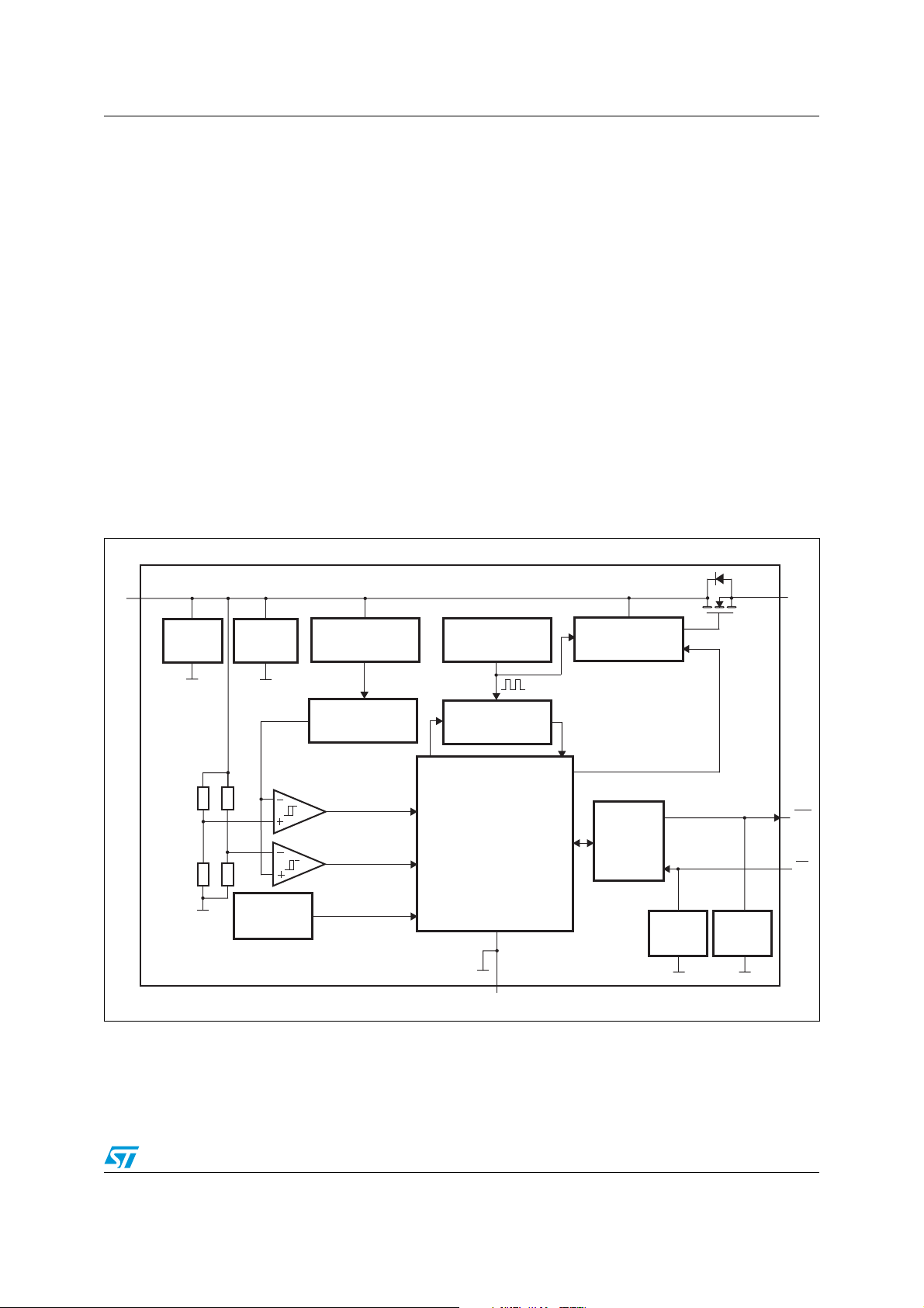
2 Description
The STBP120 provides robust protection for positive input voltage up to +28 V and is
capable of supporting current up to 2 A using a built-in low R
charge pump. The overvoltage thresholds currently available are 5.375 V, 5.50 V, 5.90 V and
6.02 V.
As additional protection, the STBP120 also monitors its own junction temperature and turns
off the internal MOSFET if the temperature exceeds the specified threshold.
The STBP120 is equipped with the undervoltage lockout function preventing unreliable
operation of the protected application for low input voltage.
The STBP120 device can be controlled (enabled / disabled) by the microcontroller and
provides status information (input overvoltage, input undervoltage, thermal shutdown)
to the microcontroller.
The STBP120 requires only one external component (1 µF input capacitor improving the
ESD immunity and stability under input transients conditions), other components are
optional (see Figure 2).
It is offered in a small, RoHS compliant 10-lead TDFN package of 2.5 x 2 mm dimensions.
For more details, please refer to the STBP120 datasheet available on www.st.com.
Figure 1. STBP120 block diagram
N-channel MOSFET and
DS(on)
IN
ESD
protection
Core
negative
protection
V
REF
Temperature
detector
SUPPLY
REGULATOR
V
CC
VOLTAGE
REFERENCE
Input overvoltage
Input undervoltage
Thermal shutdown
OSCILLATOR
COUNTERS
CONTROL LOGIC
GND
CHARGE PUMP
MOSFET DRIVER
MCU
INTERFACE
ESD
protection
OUT
OFF
FLT
EN
ESD
protection
AM00306
Doc ID 16207 Rev 1 5/18
Page 6
Application circuit AN3050
3 Application circuit
Figure 2. Typical application circuit
PERIPHERAL
AC
adapter
SYSTEM
CONNECTOR
OR
SUPPLY CURRENT
CHARGING CURRENT
IN OUT
C1
1 µF
STBP120
C2
1 µF
DC-DC
EN
CHARGER
IC
ENABLE
BATTERY
PA CK
R
SUPPLY
CIRCUITS
PU
POWERED
PERIPHERALS
FLT
EN
GND
R
R
FLT
EN
CONTROLLER
APPLICATION
AM00314a
As shown above, the right place for the OVP device is just after the system supply connector
(see Figure 2).
The input capacitor C1 plays an important role for improving the OVP functionality under fast
transients caused by hot insertion / disconnection of power supply, ESD events, etc. For fast
overvoltage transients, this capacitor acts initially as a short-circuit requiring some current to
be charged, thus making the transients slower. It also acts as a reservoir of energy in case
of fast undervoltage transients caused by the supply cable impedance when the current
drawn by the application increases, preventing the input voltage from falling below the
undervoltage threshold and cutting off the power.
After the OVP device, there is usually the charge controller IC managing proper charging
and protection of the battery back.
Normally a set of supply circuits are present to convert the battery pack voltage to the
voltage levels necessary for particular parts of the application.
A connection of STBP120 status output (FLT
) and enable input (EN) to the application
controller is also shown on Figure 2. The open-drain FLT
pull-up resistor R
to the controller supply voltage. The resistors R
PU
optional. They increase the safety of the controller in case of extreme voltage or current
condition, leading to possible damage of the STBP120, limiting the current flowing to the
controller I/O ports to a safe value (the absolute maximum voltage on the STBP120 is 30 V).
6/18 Doc ID 16207 Rev 1
output is connected by an external
and REN are
FLT
Page 7

AN3050 Powering peripherals
4 Powering peripherals
In many applications, it is desirable to power external peripherals attached to the system
connector. Proper voltage for these peripheral devices is usually generated by a DC/DC
converter supplied by the battery (see Figure 2). This converter is enabled by the controller
when power for the peripheral is requested. The output of the converter is connected to the
output of the OVP device.
In the internal structure of STBP120 MOSFET, a diode (called reverse diode or body diode)
between OUT and IN is present. This diode allows the convertor output voltage (decreased
by the diode forward voltage drop, ca. 0.6 V) to appear at the STBP120 input. If this voltage
is higher than the STBP120 undervoltage (UVLO) threshold, the MOSFET is turned on and
the voltage drop across the STBP120 is reduced to a very small value, given by the
STBP120 R
Note: For safety reasons, the charger IC used should NOT allow the reverse current (i.e. it should
NOT contain the body diode between its output and input) to prevent the battery pack
voltage from appearing on the system connector.
and peripheral current consumption.
DS(on)
Doc ID 16207 Rev 1 7/18
Page 8

STBP120 highlights AN3050
5 STBP120 highlights
The most important function of the OVP device is to disconnect the application from the
power supply as fast as possible to avoid damage to the application components.
The STBP120 will disconnect the load in typically less than 1.5 µs after the input voltage
exceeds the overvoltage threshold.
Figure 3. STBP120 turn-off delay
Input voltage
Output voltage
8/18 Doc ID 16207 Rev 1
Page 9

AN3050 STBP120 highlights
Overvoltage protection is especially necessary in order to avoid damage in the event of
inadvertently connecting an illegal power supply (with higher than specified voltage) to the
application. In this case, the OVP device must block the excessive input voltage even during
its own power-up period. As illustrated on Figure 4, STBP120 correctly performs this task. In
addition, it provides the status information to the microcontroller as soon as the input voltage
exceeds the 1.2 V.
Figure 4. Startup into overvoltage condition
Input voltage
FLT
output voltage
Output voltage
Doc ID 16207 Rev 1 9/18
Page 10

STBP120 highlights AN3050
During a hot insertion of the power supply connector to the application, a transient is
generated due to the supply cable inductance, capacitance and resistance. For this reason,
the STBP120 has a built-in 50 ms startup delay to let the input voltage to stabilize before the
MOSFET is turned on to continue power-on of the application. After this, an additional 50 ms
delay is inserted to let the application properly start before the FLT
output sends an “OK”
(SeeFigure 5) signal to the application microcontroller.
Figure 5. Startup delays
10/18 Doc ID 16207 Rev 1
Page 11

AN3050 STBP120 highlights
Usually, there are some large decoupling capacitors connected to the application supply
rails. To avoid instability caused by the power supply current limiter when attempting to
charge these capacitors, it is useful to equip the OVP device with a soft-start circuit, limiting
this inrush current. The STBP120 implements a soft-start by turning the MOSFET on slowly.
This is done by limiting the current charging the MOSFET gate capacitance. This simple
approach provides very good results for load capacitance up to 47 µF. Its performance is
illustrated in Figure 6, Figure 7 and Figure 8, where various load capacitors were connected
in parallel with the load resistor of 5 Ω, providing a steady current of 1 A.
Figure 6. Typical STBP120 soft-start performance, C
Input voltage
Output voltage
Input current
FLT
output voltage
Load
= 22 µF
Doc ID 16207 Rev 1 11/18
Page 12

STBP120 highlights AN3050
Figure 7. Typical STBP120 soft-start performance, C
Input voltage
Output voltage
Input current
FLT
output voltage
Load
= 47 µF
Figure 8. Typical STBP120 soft-start performance, C
Input voltage
Output voltage
Input current
FLT
output voltage
Load
= 100 µF
12/18 Doc ID 16207 Rev 1
Page 13

AN3050 STBP120 highlights
The soft-start circuit is very useful for USB-powered applications due to USB power
limitations. The USB specification allows a maximum inrush current equivalent to a value
generated by a 10 µF capacitor directly connected between V
and GND rails. The
BUS
STBP120 softstart feature allows an even larger capacitor value to be connected to the
STBP120 output, providing better decoupling and higher reservoir of energy to cover
possible current peaks, without affecting this requirement. Maximum capacitance proven
with a standard 2 m USB cable is 100 µF. Higher capacitance can lead to a oscillation due to
USB cable impedance and the capacitor inrush current, leading the input voltage to drop
below the UVLO threshold during the start-up. The input capacitor value can be 1 - 10 µF.
Doc ID 16207 Rev 1 13/18
Page 14

STBP120 versus Transil AN3050
6 STBP120 versus Transil
Transils are well-known and very useful protection devices for ESD events and overvoltage
transients. As mentioned in the Section 1, they can be understood as high-speed, highpower Zener diodes. Based on manufacturing process, they can achieve very high impulse
durability making them ideal for protecting e.g. AC or phone lines, or very low capacitance
making them ideal for protecting sensitive data and high frequency lines.
On the other hand, these devices are not very suitable for protection against steady-state
overvoltage on supply lines generated e.g. by connecting an illegal AC adaptor to the
application supply input, because the steady-state overvoltage generates high power
dissipation on the Transil.
Following table shows the key benefits of STBP120 device over Transils.
Table 1. Key benefits of STBP120 device over Transils
Transil device STBP120 device
Overvoltage threshold accuracy
and stability
Power dissipation when active
Undervoltage lockout Not available 3.25 V typ.
Thermal protection Not available 145 °C typ.
Status indication Not available FLT
Enable input Not available EN
Widely dependent on current,
temperature, time and process
variations
Potentially extremely high in
overvoltage
As good as ± 2.3%
Almost zero (output is safely
disconnected)
output
input
14/18 Doc ID 16207 Rev 1
Page 15

AN3050 Compatibility of STBP120 with other OVP devices
7 Compatibility of STBP120 with other OVP devices
The STBP120 is compatible with other the well known and widely used OVP devices.
The STBP120 provides the customer with the following benefits:
● Both exposed thermal pads are electrically isolated. This allows both pads to be
connected to the PCB ground plane, leading to better thermal conductivity.
● The device is equipped with a thermal shutdown feature, improving the overall
application safety.
Figure 9. Pin to pin compatibility of the STBP120
PAD1
PAD2
(1)
10
9
8
7
6
Competitor device STBP120
1
IN
PAD1
GND NC
FLAG
1. STBP120 Pin 1, PAD1 and PAD2 are not internally connected and may be tied to IN or GND.
2
GND
3
IN OUT
4
PAD2
IN
5
IN
(Top view) (Top view)
10
EN
9
8
NC
7
OUT
6
OUT
GND NC
1
NC
2
NC/GND
3
FLT
IN OUT
4
5
NC/GND
IN
EN
NC
OUT
OUT
AM00623a
Doc ID 16207 Rev 1 15/18
Page 16

PCB layout recommendations AN3050
8 PCB layout recommendations
● This device is intended as a protection device to the application from overvoltage.
It must be ensured that the clearances between PCB tracks satisfy the high voltage
design rules.
● Input capacitor, C1, should be located as close as possible to the STBP120 device.
It should be a Low-ESR ceramic capacitor. Also the protective resistors RFLT, REN
(if used) should be located close to the STBP120.
● For good thermal performance, it is recommended to connect the STBP120 exposed
thermal pads with the PCB ground plane. In most designs, this requires thermal vias
between the copper pads on PCB and the ground plane.
Figure 10. Example of PCB layout
9 Conclusion
The STBP120 device significantly increases the safety of portable electronic devices
powered (or recharged) from an external power supply by implementing fast and reliable
protection from input overvoltage. In addition it allows the system to power external
peripherals through the system connector thanks to its reverse current capability. The
STBP120 is pin to pin compatible with frequently used devices and outperforms their safety
level using the thermal shutdown protection.
16/18 Doc ID 16207 Rev 1
Page 17

AN3050 Revision history
10 Revision history
Table 2. Document revision history
Date Revision Changes
18-Nov-2009 1 Initial release.
Doc ID 16207 Rev 1 17/18
Page 18

AN3050
y
Please Read Carefully:
Informatio n in this document is provided solely in connection with ST products. STMicroelectronics NV and its subsidiaries (“ST”) reserve the
right to make changes, corrections, modifications or improvements, to this document, and the products and services described herein at an
time, without notice.
All ST products are sold pu rsuant to ST’s terms and conditions of sale.
Purchasers are solely responsible for the choice, selection a nd use of the ST products and services described herein, and ST assumes no
liability whatsoever relating to the choice, selection or use of the ST products and services described herein.
No license, express or implied, by estoppel or otherwise, to any intellectual property rights is granted under this document. If any part of this
document refers to any third party products or services it sha ll not be deemed a license grant by ST for the use of such third party products
or services, or any intellectual property contained therein or considered as a warranty covering the use in any manner whatsoever of such
third party products or services or any intellectual property contained therein.
UNLESS OTHERWISE SET FORTH IN ST’S TERMS AND CONDITIONS OF SALE ST DISCLAIMS ANY EXPRESS OR IMPLIED
WARRANTY WITH RESPECT TO THE USE AND/OR SALE OF ST PRODUCTS INCLUDING WITHOUT LIMITATION IMPLIED
WARRANTIES OF MERCHANTABILITY, FITNESS FOR A PARTICULAR PURPOSE (AND THEIR EQUIVALENTS UNDER THE LAWS
OF ANY JURISDICTION), OR INFRINGEMENT OF ANY PATENT, COPYRIGHT OR OTHER INTELLECTUAL PROPERTY RIGHT.
UNLESS EXPRESSLY APPROVED IN WRITING BY AN AUTHORIZED ST REPRESENTATIVE, ST PRODUCTS ARE NOT
RECOMMENDED, AUTHORIZED OR WARRANTED FOR USE IN MILITARY, AIR CRAFT, SPACE, LIFE SAVING, OR LIFE SUSTAINING
APPLICATIONS, NOR IN PRODUCTS OR SYSTEMS WHERE FAILURE OR MALFUNCTION MAY RESULT IN PERSONAL INJURY,
DEATH, OR SEVERE PROPERTY OR ENVIRONMENTAL DAMAGE. ST PRODUCTS WHICH ARE NOT SPECIFIED AS "AUTOMOTIVE
GRADE" MAY ONLY BE USED IN AUTOMOTIVE APPLICATIONS AT USER’S OWN RISK.
Resale of ST products with provisions differen t from the statemen ts and/or technical features set forth in this document shall i mmediately void
any warranty granted by ST for the ST product or service described herein and shall not create or extend in any manner whatsoever, any
liability of ST.
ST and the ST logo a re trademarks or registered trademarks of ST in various countries.
Information in this document supersedes and replaces all information previously supplied.
The ST logo is a registered trademark of STMicroelectronics. All other names are the property of their respective owners.
© 2009 STMicroelectro nics - All rights reserved
STMicroelectronics group of companies
Australia - Belgium - Brazil - Canada - China - Czech Republic - Finland - France - Germany - Hong Kong - India - Israel - Italy - Japan -
Malaysia - Malta - Morocco - Philippines - Singapore - Spain - Sweden - Switzerland - United Kingdom - United States of America
www.st.com
18/18 Doc ID 16207 Rev 1
 Loading...