

Page 1
AN303
Application note
Thyristors and TRIACs: latching current
Introduction
The purpose of this note is to familiarize TRIAC or thyristor (SCR) users with the latching
current I
The importance of this parameter is illustrated with some typical examples. Procedures are
given for measurement of I
sensitivity are described.
This application note presents only the TRIAC case. However, the concepts are valid for
SCRs (except for the various conduction modes).
Definition
The latching current (IL) of a TRIAC is the minimum value of the load current (current flowing
between electrodes A
removed (see Figure 1).
.
L
. The variation of IL with operating conditions and device
L
and A1) that keeps the device conducting when the gate signal is
2
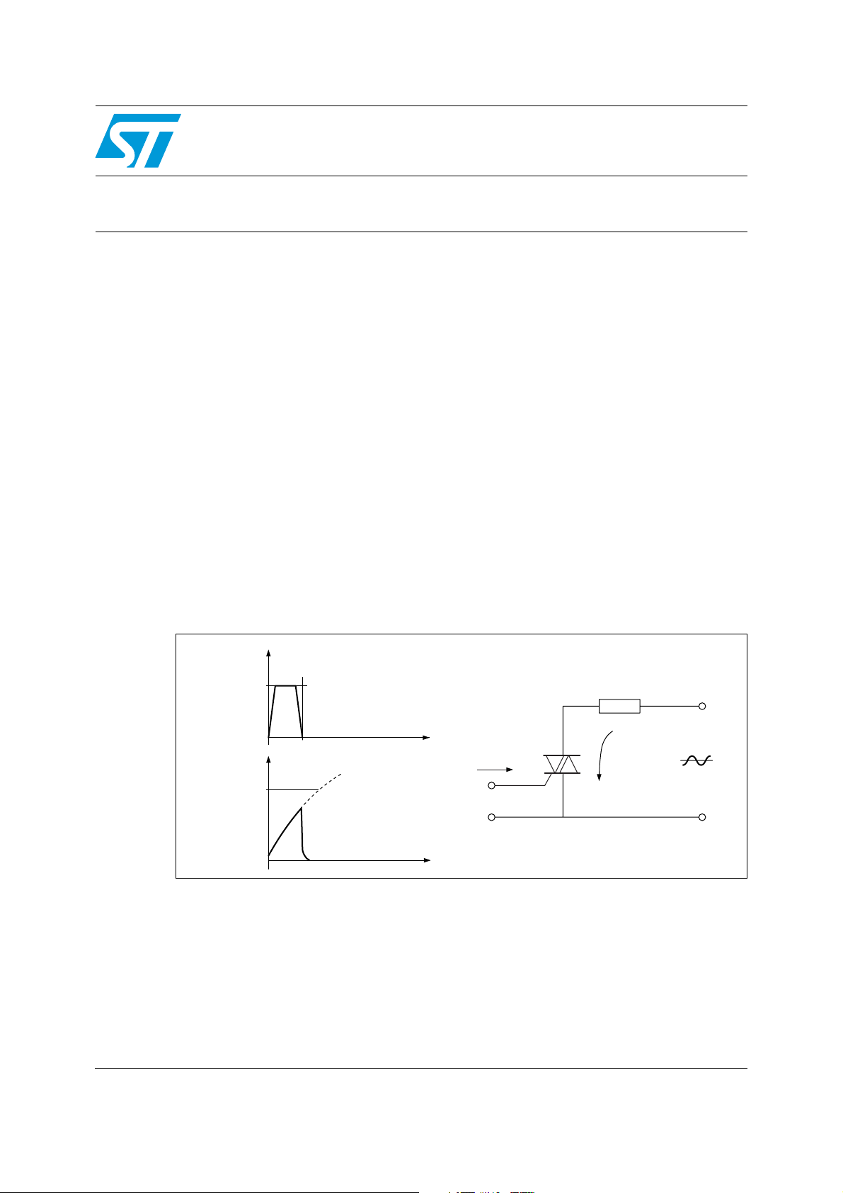
Figure 1 below shows the latching current and the gate current pulse. After the TRIAC
triggering, a current (I
the current I
is lower than the latching current IL, the TRIAC switches off.
T
) flows through the TRIAC. If the gate current (IG) is removed while
T
Figure 1. Blocked TRIAC
I
G
IG > I
GT
I
I
T
Gate current
t
I
G
L
A
A
R
L
2
I
T
1
G
Main current
t
April 2009 Doc ID 3654 Rev 3 1/13
www.st.com
Page 2
Application examples AN303
1 Application examples
The importance of the latching current is highlighted by the following application examples.
1.1 Example 1: low power lamp control
In the application circuit shown in Figure 2 a TRIAC is used to control a 10 W signaling light.
For the European mains (V
could be used to control this load current, but the maximum latching current is specified as
50 mA if a Z0110 device is used in quadrant II. The peak load current is then very close to
the maximum latching current given in the datasheet. The device will turn off if the gate
current pulse is too short.
Figure 2. Control of a low-power lamp
Lamp (10 W)
= 230 V), the peak load current is about 61 mA. A Z01 device
rms
I
T
I
L
Main
current
A
230 V
I
T
2
A
1
G
I
G
I
G
Gate
current
t
t
p
Thus, a TRIAC could not remain on if its latching current is higher than the load current at
the moment the gate current is removed (refer to Figure 2). For correct operation, a
continuous gate current should be applied or a longer gate current pulse should be applied.
For example, for a sinusoidal load current (I
the following equation (refer to AN302 for a complete definition of I
tp >
1
ω
· arcsin
I
(
HMAX
I
peak
1
· arcsin
+
)
ω
I
(
LMAX
I
peak
= I
(t)
x sin(ωt)), the pulse width is given by
peak
(a)
):
H
)
To reduce the pulse width duration, a more sensitive TRIAC could be used (for example, for
the Z0103 I
max is 15 mA in QII).
L
t
a. The minimum current that keeps a TRIAC conducting is called the hypostatic or holding current IH.
2/13 Doc ID 3654 Rev 3
Page 3
AN303 Application examples
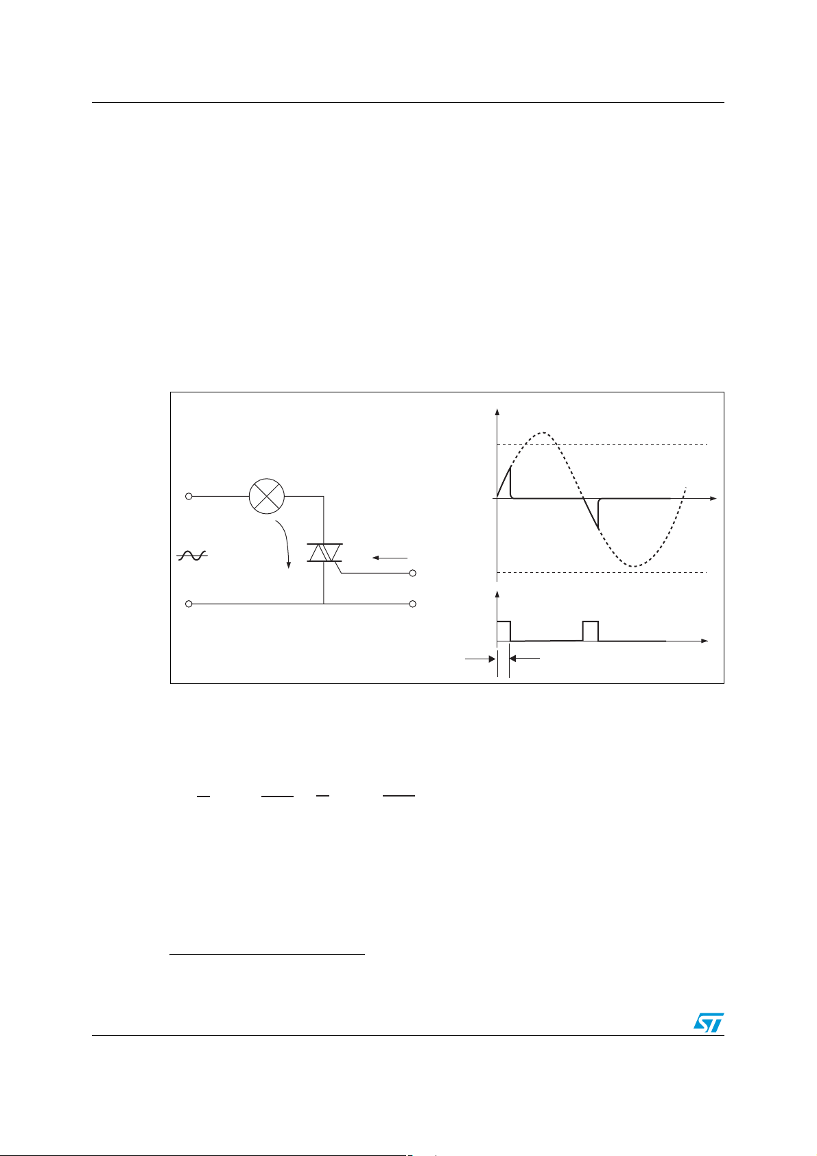
1.2 Example 2: inductive load control
When a TRIAC controls an inductive load (L), the rise of the load current IT is slowed down.
The approximate load current slope dI
dI
V
T
A
~
=
dt
L
/dt is given by:
T
where V
is the mains voltage when the gate signal is applied.
A
In Figure 3 the impact of the gate pulse width on the TRIAC conduction is shown.
● In continuous lines: A short gate signal (T1) is applied. The TRIAC doesn’t remain in
the on state because the load current I
doesn’t reach the TRIAC latching current level
T
before the gate current removal.
● In dotted lines: A longer gate signal (T2) is applied. In this case, the TRIAC turns on
and remains in the on state. The TRIAC turns off when the load current reaches zero
after the gate current removal.
Figure 3. Control of an alternating current (AC) motor
M
A
I
T
V
I
G
V
T
V
A
2
I
T
A
1
T
1
G
G
T
2
t
t
I
G
I
L
t
For correct operation a gate current has to be applied until the load current reaches the
TRIAC latching current. The control mode shown in Figure 3 is a square pulse.
Another TRIAC control mode is to apply a gate pulse train. Application note AN308 offers
some TRIAC control circuits specially designed to work with inductive loads.
Doc ID 3654 Rev 3 3/13
Page 4
Application examples AN303
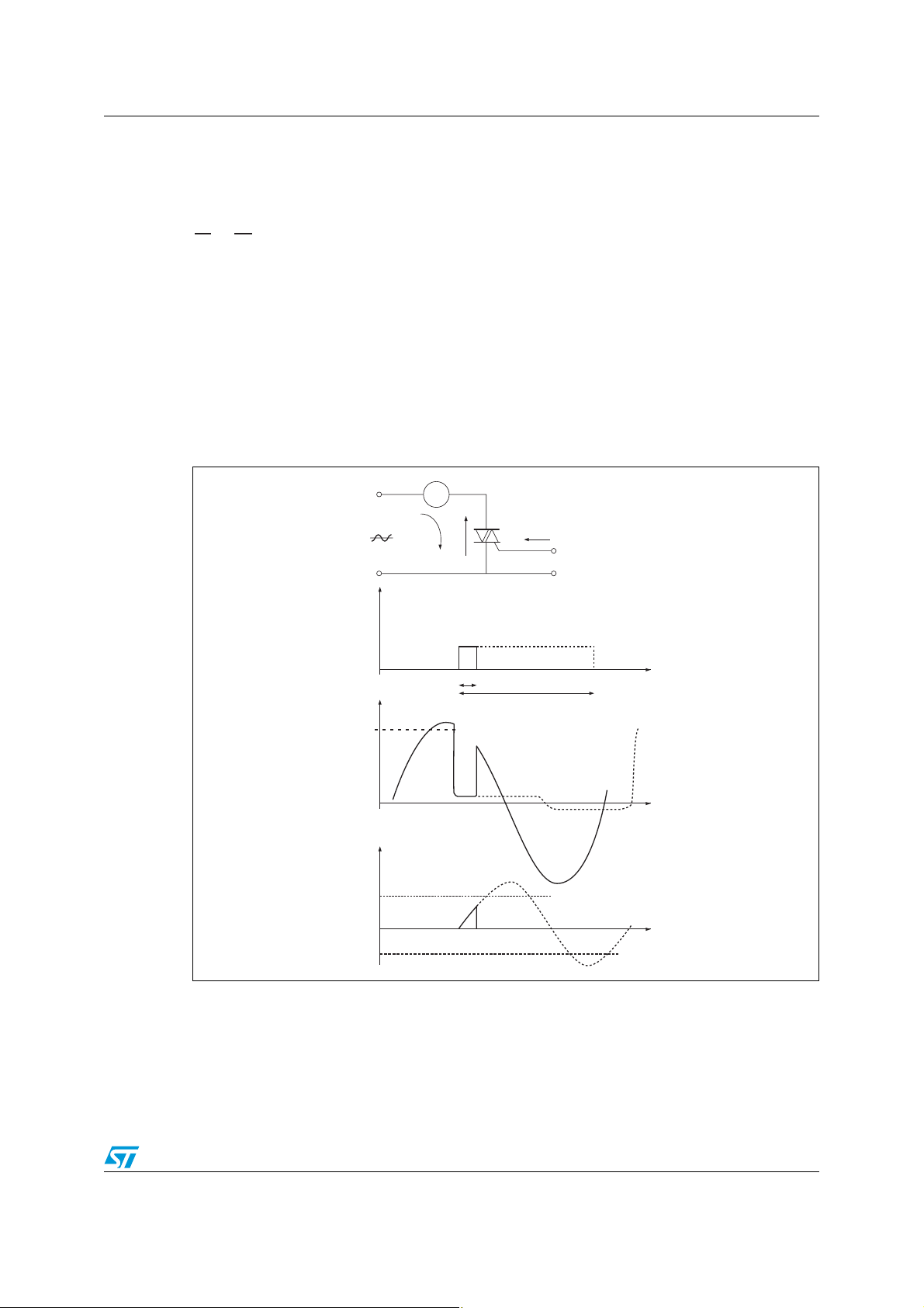
1.3 Example 3: varying power load control
For most applications, the load power is controlled by the TRIAC conduction time. For arc
welding (see Figure 4), the controlled power can be subjected to considerable variations.
The device current rating is chosen and validated for full-wave and full load operation. The
application operation is then ensured in the worst case but, for low power loads, a TRIAC
triggering issue could occur.
In the case of an open load operation, the load current equals the transformer magnetizing
current, which is much lower than full load current. The load current could even be below the
TRIAC latching current in one triggering quadrant. Thus, the TRIAC could turn on properly in
one quadrant but could not turn on in another quadrant, for which the latching current is
higher. An unbalance then occurs and induces a direct current (DC) through the
transformer, which heats its coils and can cause transformer failure.
For correct circuit design, the TRIAC operation should be validated in full load and also in
open load. (See AN308 for a schematic circuit diagram dedicated to this welding
application.)
Figure 4. Arc welding control
A
G
2
A
1
4/13 Doc ID 3654 Rev 3
Page 5

AN303 Latching current – the details
2 Latching current – the details
The three examples in the previous section illustrate the importance of the latching current
parameter and the different issues considered in taken into account the latching current
requirements.
In STMicroelectronics’ datasheets for all types of TRIACs or SCRs the latching current (I
specified as a maximum value for a 25 °C junction temperature. Then corrections have to be
made according to temperature variations.
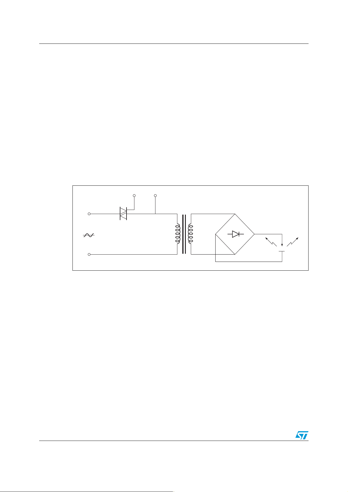
2.1 Effect of RC snubber circuit at turn on
For most applications, an RC snubber across TRIAC A2 and A1 terminals is used to
improve TRIAC immunity to fast transient voltages and also, in the case of inductive loads,
to ensure appropriate TRIAC turn off. (Refer to Figure 5 and AN437 for RC snubber circuit
design for TRIACs.)
Figure 5. RC snubber circuit.
I
T
A
2
A
G
1
C
R
In the case of inductive loads, an RC snubber has another advantage at TRIAC turn on. The
energy stored in the snubber capacitor C, during the TRIAC off state, is fed back through the
TRIAC at turn on. The TRIAC current slope during the capacitor discharge is proportional to
the capacitor voltage before the TRIAC turn on and inversely proportional to the series
inductances of the board and the snubber resistor. Thus, the TRIAC current rise is faster
than the load current and reaches the device latching current in a shorter time (see
Figure 6).
LI
I
C
L
) is
Figure 6. Snubber capacitor discharge at TRIAC turn on
I
I
T1
I
T
current
I
L
level
I
dIT/dt
Doc ID 3654 Rev 3 5/13
I : Current in the load
I
C: Discharge current of capacitor C
IT:I +IC: Current in the TRIAC
I
C
t
Page 6
Latching current – the details AN303
Note: To limit the rate of current rise at turn on (dIT/dt) during the capacitor discharge, the value of
the resistor (R) must be higher than a minimum value (typically 47 ohms for most TRIACs).
A higher dI
peak current (I
/dt than the dI/dt specified in the datasheet may damage the device. The TRIAC
T
) is approximately the quotient of the capacitor voltage and the snubber
T1
resistance.
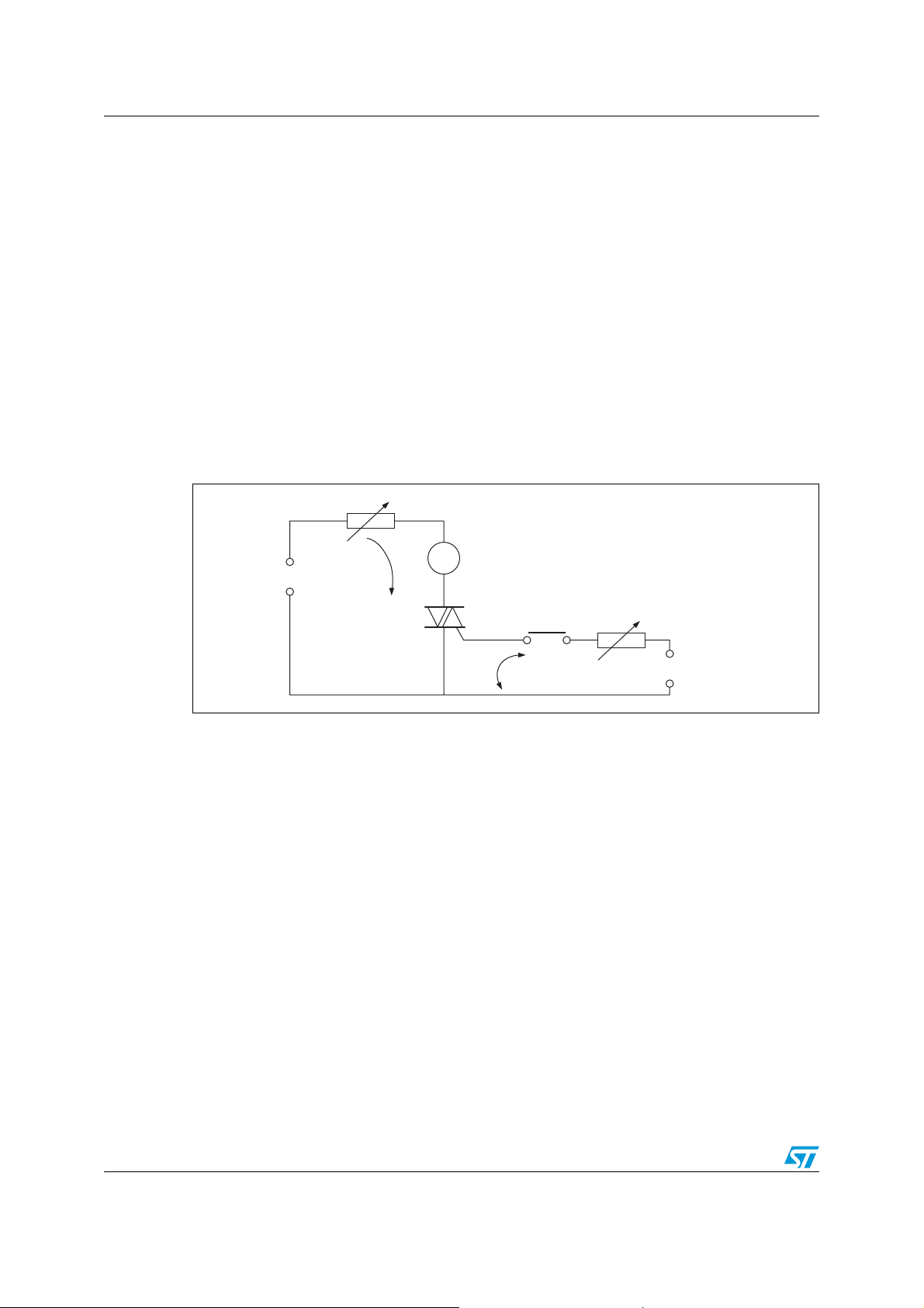
2.2 Latching current measurement
In Figure 7, push button C is used to trigger the TRIAC. The value of the gate current I
set to a higher value than the gate current specified in the datasheet (I
Decreasing the resistance R causes the TRIAC current I
latching current I
is the value of the TRIAC current IT when the TRIAC remains on without a
L
to increase. The value of the
T
= 1.2 x IGT).
G
gate current.
Sensitive SCRs, that is, those with a gate triggering current I
of 200 µA or less, are
GT
measured with a 1 kΩ resistor connected between gate and cathode.
Figure 7. Circuit for the measurement of the latching current (I
R
I
≥33Ω
1
G
R
C
2
V = ±12V
R
1
I
T
A
A
2
A
1
G
)
L
V = ±12V
For repeatable results, the TRIAC should be appropriately turned on. The following
guidelines must be applied:
● The pulse width of the gate current must be at least equal to 1 ms.
● The applied gate current (I
(I
) of the device measured. An IG / I
GT
) must by higher than the specified triggering gate current
G
ratio higher than or equal to 1.2 is
GT
recommended.
is
G
There are four different latching current levels; corresponding to the four triggering
quadrants (refer to Figure 8). These quadrants are defined according to V
positive if A2 is set to a higher bias voltage than A1) and gate polarity (I
sourced to the gate, so it circulates from G to A1):
● Quadrant I (QI): V
● Quadrant II (QII): V
● Quadrant III (QIII): V
● Quadrant IV (QIV): V
I
in QIV is not specified for devices only controlled in the three first quadrants, as
L
Snubberless
TM: Snubberless is a trademark of STMicroelectronics
TM
, logic level and high temperature TRIACs.
6/13 Doc ID 3654 Rev 3
> 0 and IG > 0
T
> 0 and IG < 0
T
< 0 and IG < 0
T
< 0 and IG > 0
T
polarity (VT is
T
is positive if it is
G
Page 7

AN303 Latching current – the details
Figure 8. TRIAC triggering quadrants
V
T
A
2
V
T
I
G
A
1
QIII
--
+-
QII
+ +
QI
QIV
-+
I
G
2.3 Variation of the latching current
2.3.1 Typical variation of IL with device sensitivity and quadrant
The latching current IL is related to the triggering current, IGT. The IL/IGT ratio also depends
on the triggering quadrant as shown in Tab le 1 .
Table 1. Approximate ratio between IL and IGT for sensitive and standard TRIACs
Sensitive TRIAC 12 A rms (TW type) 3 6 3.5 N.A.
Standard TRIAC 12 A rms (C type) 1.5 4.5 1 0.5
Example
With a BTA/BTB12-600TW, IGT (QI) = 1 mA (measured),
then I
(QI) ≈ 3 mA, IL (QII) ≈ 6 mA and IL (QIII) ≈ 3.5 mA.
L
With a BTA/BTB12-600C, I
then I
(Q1) ≈ 22.5 mA, IL (QII) ≈ 67.5 mA, IL (QIII) ≈ 15 mA and IL (QIV) ≈ 7.5 mA.
L
(QI) = 15 mA (measured),
GT
In the case of TRIACs (as opposed to the SCRs), it is important to note that the current I
(QII), is much higher than the I
current in the other quadrants. So, in the data sheets, two
L
maximum values are specified: one value for quadrants I, III and IV (if specified) and one
value for quadrant II.
2.3.2 Typical variation between IL and I
The holding current value I
current value I
than the I
Table 2. Approximate ratio between IL and IH according to devices current rating
. For the most TRIACs (rated current lower than 40 A), the I
L
value. The IL/I
H
(refer to AN302 for holding current) is linked to the latching
H
ratio is related to the TRIACs current rating, as shown Ta bl e 2.
H
H
I (QI)
L
I (QI)
GT
I (QII)
L
I (QII)
GT
I (QIII)
L
I (QIII)
GT
value is higher
L
I (QIV)
L
I (QIV)
GT
L
(1)
/ I
I
L
H
I
≤ 6 A 6 A ≤ I
RMS
RMS
1.1 to 1.5 1.5 to 3
≤ 40 A
1. First quadrant in the case of TRIACs
Doc ID 3654 Rev 3 7/13
Rating of TRIACs and SCRs
Page 8

Latching current – the details AN303
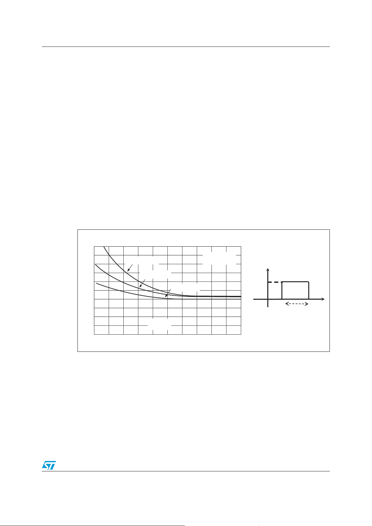
2.3.3 Typical variation of IL with junction temperature
The latching current is physically related to the triggering gate current IGT. These two
parameters vary with the junction temperature as shown in Figure 9.
Figure 9. Relative variation of I
with the junction temperature T
L
Example
With a BTA12-600C,
I
(QI) = 20 mA (measured) at T
L
= 25 °C, then I
j
(QI) ≈ 32.5 mA at T
L
2.3.4 Influence of the external gate-cathode resistor
In some applications, an RGK resistor is connected between the gate and the cathode of the
component. This resistor either improves device behavior under fast transient voltages (bypass for A2-G leakage current) in the case of sensitive SCRs or forms part of the triggering
circuit. The value of this resistor, as well as the sensitivity of the component, affects the
latching current as shown in Figure 10.
j
= – 40 °C.
j
Figure 10. Variation of I
IL[R
] / IL[RGK= 1 k
GK
, for a sensitive SCR with RGK
L
Ω]
10
9
8
7
6
5
4
3
2
1
0
R(k)
Ω
GK
0.01 0.10 1.00 10.00
8/13 Doc ID 3654 Rev 3
Tj= 25 °C
Sensitive SCR
Page 9
AN303 Latching current – the details
Note: The latching current of sensitive SCRs is always specified with a 1000 ohm gate-cathode
resistor.
Sensitive SCRs (I
< 200 µA)
GT
For sensitive SCRs, RGK has a large influence on the latching current as shown by
Figure 10. Thus, in certain applications, the designer may want to use a high-impedance
control circuit. The drawback will then be that the SCR sustainable dV/dt will be lower.
Standard SCRs, sensitive and standard TRIACs
RGK greater than 20 Ω will have no significant effect on the latching. But values lower than
20 Ω are not used in practice as they will excessively increase the current applied by the
control circuit to trigger the device.
2.3.5 Typical variation of the latching current IL with the control signal
The latching current IL varies with the amplitude and the pulse width tp of the gate current IG.
With a constant triggering pulse width (< 50 µs), the I
amplitude increase. And vice versa, if the I
lead to the I
Figure 11. Variation of I
amplitude increase (refer to Figure 11).
L
with the width tp and the amplitude IG of the gate pulse
L
amplitude is kept constant, the tp decrease will
G
(quadrant I)
TRIAC BTB16-600B
GT
IG= 5 I
GT
IG= 2 I
t
(µs)
p
30
Tj= 25 °C
GT
40
100
90
80
70
60
50
40
30
20
10
IL(mA)
0
0
IG= 10 I
10 20
amplitude increase will lead to the IL
G
I
G
I
GT
t
p
[pulse width]
50
t
The latching current varies also according to the gate current pulse shape. The latching
current can:
● Increase if a negative gate current is applied at the end of the pulse, as shown in
Figure 12.
● Decrease if the decreasing slope of the gate current is low (compared to dashed line),
as shown in Figure 13. For a decreasing slope of the gate current lower than 0.5 A/µs,
the I
value is typically closed to the IH value.
L
Doc ID 3654 Rev 3 9/13
Page 10

Latching current – the details AN303
Figure 12. Gate current pulse with negative current at the end of the pulse
I
G
Figure 13. Gate current pulse with smooth decreasing slope of the gate current
I
G
To ensure a suitable device triggering, an I
(calculated for the minimum application ambient temperature, see Figure 9) and an I
amplitude of 1.2 times the specified IGT
G
pulse
G
width as high as possible are recommended. A control pulse with decreasing slope of the
gate current, and without reverse current, allows the latching current to decrease.
10/13 Doc ID 3654 Rev 3
Page 11

AN303 Conclusion
3 Conclusion
The SCR or TRIAC choice does not depend only on the voltage, the rated current and the
sensitivity. Other parameters must be taken into account to ensure appropriate operation.
Among them, the latching current, I
The value of this parameter varies with
● gate current pulse (amplitude, shape and width)
● temperature
● control circuit (in the case of sensitive SCRs)
● direction of current flow
TRIAC and SCR applications, involving highly inductive loads or loads with considerable
power variations, are the main applications for which the latching current must be given
particular consideration.
Taking into account these aspects, the designer can obtain satisfactory operation of the
circuit in industrial applications.
, plays an important role in many circuits.
L
Doc ID 3654 Rev 3 11/13
Page 12

Revision history AN303
4 Revision history
Table 3. Document revision history
Date Revision Changes
Apr-1995 1 First issue.
15-May-2004 2 Style sheet update. No content change.
24-Apr-2009 3
Reformatted to current standards. Complete technical update for
current devices.
12/13 Doc ID 3654 Rev 3
Page 13

AN303
Please Read Carefully:
Information in this document is provided solely in connection with ST products. STMicroelectronics NV and its subsidiaries (“ST”) reserve the
right to make changes, corrections, modifications or improvements, to this document, and the products and services described herein at any
time, without notice.
All ST products are sold pursuant to ST’s terms and conditions of sale.
Purchasers are solely responsible for the choice, selection and use of the ST products and services described herein, and ST assumes no
liability whatsoever relating to the choice, selection or use of the ST products and services described herein.
No license, express or implied, by estoppel or otherwise, to any intellectual property rights is granted under this document. If any part of this
document refers to any third party products or services it shall not be deemed a license grant by ST for the use of such third party products
or services, or any intellectual property contained therein or considered as a warranty covering the use in any manner whatsoever of such
third party products or services or any intellectual property contained therein.
UNLESS OTHERWISE SET FORTH IN ST’S TERMS AND CONDITIONS OF SALE ST DISCLAIMS ANY EXPRESS OR IMPLIED
WARRANTY WITH RESPECT TO THE USE AND/OR SALE OF ST PRODUCTS INCLUDING WITHOUT LIMITATION IMPLIED
WARRANTIES OF MERCHANTABILITY, FITNESS FOR A PARTICULAR PURPOSE (AND THEIR EQUIVALENTS UNDER THE LAWS
OF ANY JURISDICTION), OR INFRINGEMENT OF ANY PATENT, COPYRIGHT OR OTHER INTELLECTUAL PROPERTY RIGHT.
UNLESS EXPRESSLY APPROVED IN WRITING BY AN AUTHORIZED ST REPRESENTATIVE, ST PRODUCTS ARE NOT
RECOMMENDED, AUTHORIZED OR WARRANTED FOR USE IN MILITARY, AIR CRAFT, SPACE, LIFE SAVING, OR LIFE SUSTAINING
APPLICATIONS, NOR IN PRODUCTS OR SYSTEMS WHERE FAILURE OR MALFUNCTION MAY RESULT IN PERSONAL INJURY,
DEATH, OR SEVERE PROPERTY OR ENVIRONMENTAL DAMAGE. ST PRODUCTS WHICH ARE NOT SPECIFIED AS "AUTOMOTIVE
GRADE" MAY ONLY BE USED IN AUTOMOTIVE APPLICATIONS AT USER’S OWN RISK.
Resale of ST products with provisions different from the statements and/or technical features set forth in this document shall immediately void
any warranty granted by ST for the ST product or service described herein and shall not create or extend in any manner whatsoever, any
liability of ST.
ST and the ST logo are trademarks or registered trademarks of ST in various countries.
Information in this document supersedes and replaces all information previously supplied.
The ST logo is a registered trademark of STMicroelectronics. All other names are the property of their respective owners.
© 2009 STMicroelectronics - All rights reserved
Australia - Belgium - Brazil - Canada - China - Czech Republic - Finland - France - Germany - Hong Kong - India - Israel - Italy - Japan -
STMicroelectronics group of companies
Malaysia - Malta - Morocco - Philippines - Singapore - Spain - Sweden - Switzerland - United Kingdom - United States of America
www.st.com
Doc ID 3654 Rev 3 13/13
 Loading...