

Page 1
AN3024
Application note
SPC560B4x/5x, SPC560C4x/5x hardware design guideline
Introduction
This application note complements the information in the SPC560Bxx and SPC560Cxx
device datasheet (see Section Appendix A: Document management) by describing
requirements useful for a hardware implementation of the development board features such
as power supply, reset control, clock management, boot mode setting, debug management
and I/Os settings. It shows how to use the product and defines the minimum hardware
resources required to start an application development.
Sections of this document describe certain device features in brief without describing the
device blocks in detail. For a detailed description of these features, refer to the device
datasheet, the reference manual RM0017 or the SPC560Bxx and SPC560Cxx errata sheet,
or all three documents (see Section A.1: Reference documents).
This application note applies to the SPC560Bxx and SPC560Cxx devices listed in Ta b le 1 .
T a ble 1. Device summary
Reference Part number
SPC560B4x
SPC560B5x
SPC560C4x
SPC560C5x
SPC560B40L3, SPC560B40L5, SPC560B44L3
SPC560B50L3, SPC560B50L5, SPC560B50B2
SPC560C40L3, SPC560C44L3
SPC560C50L3
June 2012 Doc ID 16127 Rev 3 1/27
www.st.com
Page 2

Contents AN3024
Contents
1 Power supplies . . . . . . . . . . . . . . . . . . . . . . . . . . . . . . . . . . . . . . . . . . . . . 6
1.1 Introduction . . . . . . . . . . . . . . . . . . . . . . . . . . . . . . . . . . . . . . . . . . . . . . . . 6
1.2 Power supply scheme . . . . . . . . . . . . . . . . . . . . . . . . . . . . . . . . . . . . . . . . 7
1.3 Current consumption and voltage regulator . . . . . . . . . . . . . . . . . . . . . . . . 7
1.4 Layout recommendations . . . . . . . . . . . . . . . . . . . . . . . . . . . . . . . . . . . . . . 8
2 Reset . . . . . . . . . . . . . . . . . . . . . . . . . . . . . . . . . . . . . . . . . . . . . . . . . . . . . . 9
2.1 Introduction . . . . . . . . . . . . . . . . . . . . . . . . . . . . . . . . . . . . . . . . . . . . . . . . 9
2.2 Power-on reset (POR) and low voltage detectors (LVDs) . . . . . . . . . . . . . 10
2.3 System reset pin . . . . . . . . . . . . . . . . . . . . . . . . . . . . . . . . . . . . . . . . . . . . 10
2.3.1 Input characteristics . . . . . . . . . . . . . . . . . . . . . . . . . . . . . . . . . . . . . . . . 10
2.3.2 Output characteristics . . . . . . . . . . . . . . . . . . . . . . . . . . . . . . . . . . . . . . 11
2.4 Reset scheme . . . . . . . . . . . . . . . . . . . . . . . . . . . . . . . . . . . . . . . . . . . . . 11
3 ADC . . . . . . . . . . . . . . . . . . . . . . . . . . . . . . . . . . . . . . . . . . . . . . . . . . . . . . 13
3.1 Introduction . . . . . . . . . . . . . . . . . . . . . . . . . . . . . . . . . . . . . . . . . . . . . . . 13
3.2 ADC performances optimization . . . . . . . . . . . . . . . . . . . . . . . . . . . . . . . . 14
4 External oscillators . . . . . . . . . . . . . . . . . . . . . . . . . . . . . . . . . . . . . . . . . 15
4.1 Introduction . . . . . . . . . . . . . . . . . . . . . . . . . . . . . . . . . . . . . . . . . . . . . . . 15
4.2 Fast external crystal oscillator (4 to 16 MHz) . . . . . . . . . . . . . . . . . . . . . . 15
4.3 Slow external crystal oscillator (32 kHz) . . . . . . . . . . . . . . . . . . . . . . . . . 16
4.3.1 Some recommended crystal . . . . . . . . . . . . . . . . . . . . . . . . . . . . . . . . . 16
4.4 Layout recommendations . . . . . . . . . . . . . . . . . . . . . . . . . . . . . . . . . . . . . 16
5 Boot configuration . . . . . . . . . . . . . . . . . . . . . . . . . . . . . . . . . . . . . . . . . 18
5.1 Introduction . . . . . . . . . . . . . . . . . . . . . . . . . . . . . . . . . . . . . . . . . . . . . . . 18
5.2 Boot mode selection . . . . . . . . . . . . . . . . . . . . . . . . . . . . . . . . . . . . . . . . . 18
5.3 Boot pin scheme . . . . . . . . . . . . . . . . . . . . . . . . . . . . . . . . . . . . . . . . . . . . 19
6 Debug . . . . . . . . . . . . . . . . . . . . . . . . . . . . . . . . . . . . . . . . . . . . . . . . . . . . 20
6.1 Introduction . . . . . . . . . . . . . . . . . . . . . . . . . . . . . . . . . . . . . . . . . . . . . . . 20
6.2 JTAG I/Os . . . . . . . . . . . . . . . . . . . . . . . . . . . . . . . . . . . . . . . . . . . . . . . . . 20
2/27 Doc ID 16127 Rev 3
Page 3

AN3024 Contents
6.3 JTAG connector scheme . . . . . . . . . . . . . . . . . . . . . . . . . . . . . . . . . . . . . 20
7 I/Os . . . . . . . . . . . . . . . . . . . . . . . . . . . . . . . . . . . . . . . . . . . . . . . . . . . . . . 21
7.1 Introduction . . . . . . . . . . . . . . . . . . . . . . . . . . . . . . . . . . . . . . . . . . . . . . . 21
7.2 I/O types . . . . . . . . . . . . . . . . . . . . . . . . . . . . . . . . . . . . . . . . . . . . . . . . . . 21
7.3 I/Os configuration after reset . . . . . . . . . . . . . . . . . . . . . . . . . . . . . . . . . . 21
7.4 Maximum output current . . . . . . . . . . . . . . . . . . . . . . . . . . . . . . . . . . . . . . 22
7.5 I/O characteristic in STANDBY mode . . . . . . . . . . . . . . . . . . . . . . . . . . . . 22
7.6 General consideration for I/O . . . . . . . . . . . . . . . . . . . . . . . . . . . . . . . . . . 23
8 EMC guidelines . . . . . . . . . . . . . . . . . . . . . . . . . . . . . . . . . . . . . . . . . . . . 24
8.1 SPC560Bxx/Cxx software configurations . . . . . . . . . . . . . . . . . . . . . . . . . 24
8.2 Hardware guidelines . . . . . . . . . . . . . . . . . . . . . . . . . . . . . . . . . . . . . . . . . 24
9 Reference schematic . . . . . . . . . . . . . . . . . . . . . . . . . . . . . . . . . . . . . . . 26
Appendix A Document management . . . . . . . . . . . . . . . . . . . . . . . . . . . . . . . . . . 27
A.1 Reference documents . . . . . . . . . . . . . . . . . . . . . . . . . . . . . . . . . . . . . . . . 27
A.2 Acronyms . . . . . . . . . . . . . . . . . . . . . . . . . . . . . . . . . . . . . . . . . . . . . . . . . 27
Revision history . . . . . . . . . . . . . . . . . . . . . . . . . . . . . . . . . . . . . . . . . . . . . . . . . . . . 28
Doc ID 16127 Rev 3 3/27
Page 4

List of tables AN3024
List of tables
Table 1. Device summary . . . . . . . . . . . . . . . . . . . . . . . . . . . . . . . . . . . . . . . . . . . . . . . . . . . . . . . . . . 1
Table 2. Recomanded crystal . . . . . . . . . . . . . . . . . . . . . . . . . . . . . . . . . . . . . . . . . . . . . . . . . . . . . . 16
Table 3. Boot mode selection . . . . . . . . . . . . . . . . . . . . . . . . . . . . . . . . . . . . . . . . . . . . . . . . . . . . . . 19
Table 4. I/O supply segment. . . . . . . . . . . . . . . . . . . . . . . . . . . . . . . . . . . . . . . . . . . . . . . . . . . . . . . 22
Table 5. Acronyms . . . . . . . . . . . . . . . . . . . . . . . . . . . . . . . . . . . . . . . . . . . . . . . . . . . . . . . . . . . . . . 27
Table 6. Document revision history . . . . . . . . . . . . . . . . . . . . . . . . . . . . . . . . . . . . . . . . . . . . . . . . . 28
4/27 Doc ID 16127 Rev 3
Page 5

AN3024 List of figures
List of figures
Figure 1. Power supply overview . . . . . . . . . . . . . . . . . . . . . . . . . . . . . . . . . . . . . . . . . . . . . . . . . . . . . 6
Figure 2. Power supply scheme. . . . . . . . . . . . . . . . . . . . . . . . . . . . . . . . . . . . . . . . . . . . . . . . . . . . . . 7
Figure 3. Typical layout for VDD/VSS pair . . . . . . . . . . . . . . . . . . . . . . . . . . . . . . . . . . . . . . . . . . . . . . 8
Figure 4. System reset and low power circuitry . . . . . . . . . . . . . . . . . . . . . . . . . . . . . . . . . . . . . . . . . 10
Figure 5. Noise filtering on reset signal . . . . . . . . . . . . . . . . . . . . . . . . . . . . . . . . . . . . . . . . . . . . . . . 11
Figure 6. Reference reset circuit . . . . . . . . . . . . . . . . . . . . . . . . . . . . . . . . . . . . . . . . . . . . . . . . . . . . 12
Figure 7. ADC input scheme . . . . . . . . . . . . . . . . . . . . . . . . . . . . . . . . . . . . . . . . . . . . . . . . . . . . . . . 13
Figure 8. Input equivalent circuit . . . . . . . . . . . . . . . . . . . . . . . . . . . . . . . . . . . . . . . . . . . . . . . . . . . . 14
Figure 9. Reference oscillator circuit . . . . . . . . . . . . . . . . . . . . . . . . . . . . . . . . . . . . . . . . . . . . . . . . . 15
Figure 10. Low power oscillator and resonator connection scheme . . . . . . . . . . . . . . . . . . . . . . . . . . 16
Figure 11. Oscillator circuitry layout. . . . . . . . . . . . . . . . . . . . . . . . . . . . . . . . . . . . . . . . . . . . . . . . . . . 17
Figure 12. Boot mode selection . . . . . . . . . . . . . . . . . . . . . . . . . . . . . . . . . . . . . . . . . . . . . . . . . . . . . . 18
Figure 13. Boot mode selection implementation example . . . . . . . . . . . . . . . . . . . . . . . . . . . . . . . . . . 19
Figure 14. JTAG connector scheme . . . . . . . . . . . . . . . . . . . . . . . . . . . . . . . . . . . . . . . . . . . . . . . . . . 20
Figure 15. Typical application schematic . . . . . . . . . . . . . . . . . . . . . . . . . . . . . . . . . . . . . . . . . . . . . . . 26
Doc ID 16127 Rev 3 5/27
Page 6
Power supplies AN3024
1 Power supplies
1.1 Introduction
The device requires a 3.3 V or 5.0 V operating voltage supply (high voltage). An embedded
regulator is used to supply the internal 1.2 V digital power (low voltage).
Three different high voltage pin supply types are used:
● VDD_HV—high voltage external power supply for internal voltage regulators, I/O pins
and Flash
● VDD_BV—high voltage external power supply for internal voltage regulator ballast
transistors
● VDD_HV_ADC—high voltage external power supply for analog-to-digital converter
Three different independent voltage regulators provide the 1.2 V digital power supply:
● HPREG—high power internal voltage regulator used during normal operations. It can
be switched off in STOP mode and is automatically switched off in STANDBY mode.
● LPREG—low power internal voltage regulator used when HPREG is off. It can be
switched off in STOP mode and is automatically switched off in STANDBY mode.
● ULPREG—ultra low power internal voltage regulator. Always switched on and used in
STANDBY or in STOP mode when all other regulators are switched off.
External capacitors connected between the VDD_LV/VSS_LV pin pairs ensure the stability
of the internal 1.2 V HPREG and LPREG regulators.
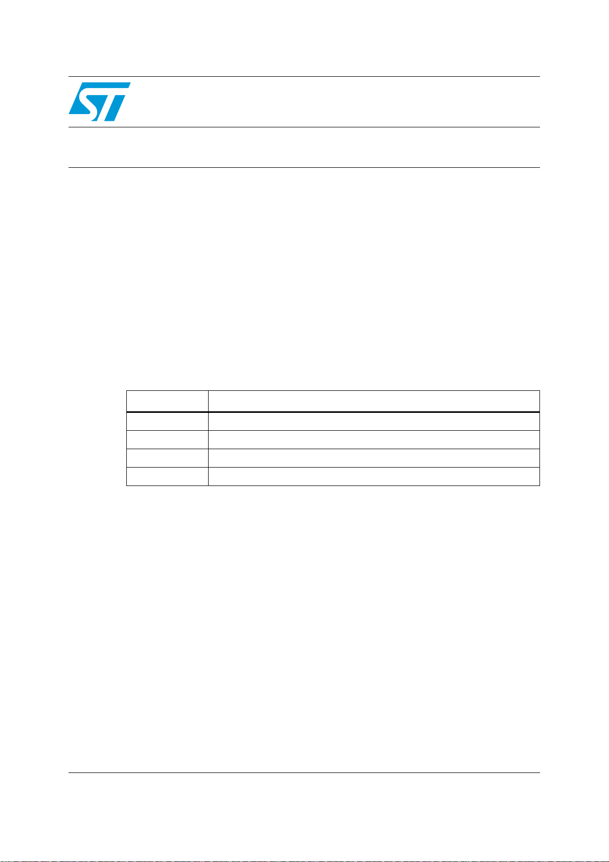
Figure 1. Power supply overview
V
DD
VDD_BV
C
BAL
ctrl
ULPREG
V
DD
C
C
VDD_HV
DECn
VDD_LV
REGm
ctrl
LPREG
ctrl
HPREG
8-KB SRAM
WKPU
RC
24-KB SRAM
CFlash
DFlash
PLL
Power Domain 0
Power Domain 2
16-KB SRAM
Core
Power Domain 1
OSC
Peripherals
Standby
Standby
Peripherals
Main
ADC
VDD_HV_ADC
VSS_HV_ADC
V
DD
For a detailed list of supply-related pins for all packages, please refer to the voltage supply
pins section in RM0017 (see Section A.1: Reference document).
6/27 Doc ID 16127 Rev 3
Page 7
AN3024 Power supplies
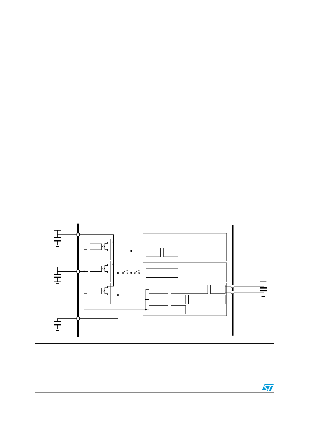
1.2 Power supply scheme
The circuit is powered by a stabilized power supply VDD.
● VDD_HV pins must be connected to V
● VDD_BV pin must be connected to V
● VDD_HV_ADC pin be connected to V
● VDD_LV pins must be connected with external decoupling capacitors C
close as possible to the device pins.
● VSS_HV and VSS_LV pins must all be connected together to GND.
Refer to the voltage regulator electrical characteristics section in the device datasheet (see
Section A.1: Reference document) for exact capacitor values.
Figure 2. Power supply scheme
with external decoupling capacitors C
DD
with external decoupling capacitor C
DD
with external decoupling capacitor C
DD
REGm
.
DECn
.
BAL
.
ADC
placed as
V
DD
C
BAL
V
DD
C
DECn
C
REGm
Note:
The device cannot be supplied with external 1.2 V. The on-chip regulator must always be used.
VDD_BV
VDD_HV 1/2/../n
VSS_HV 1/2/../n
VDD_LV 1/2/../m
VSS_LV 1/2/../m
SPC560B/C4/5x
VDD_HV_ADC
VSS_HV_ADC
V
DD
C
ADC
Caution: All BV and HV and ADC supplies must be powered with a voltage level in the range
V
± 0.1 V, and all grounds must be in the range V
DD
SS
± 0.1 V.
1.3 Current consumption and voltage regulator
In order to select a suitable external voltage regulator and design a supply circuit, the
designer of the application must consider:
1. The maximum consumption in steady state
2. The maximum inrush current during device start-up
The maximum consumption in steady state depends on the frequency of the CPU, the
usage of the peripheral and the current drawn by the outputs. It can be estimated by
referring to the device datasheet (see Section A.1: Reference document).
Doc ID 16127 Rev 3 7/27
Page 8
Power supplies AN3024
The inrush current required by the device during power-on reset or exit from STANDBY is
clamped at 400 mA and lasts for few microseconds (maximum 20 µs
) until the C
REGm
stabilization capacitors (total value ~1 µF) are charged. This current is drawn from the
VDD_BV pin.
Note: The inrush current must be considered to dimension the decoupling capacitance of the
ballast (C_DEC1) value as during this inrush the application must ensure V
remains in
DD
the voltage range of the application (5 V or 3.3 V ±10 %). The steady current is used to
define the voltage regulator capability of the application.
1.4 Layout recommendations
All the supply connections, including pads, tracks and vias, must have impedance as low as
possible (less than 5 nH). This is typically achieved by using thick and wide Cu tracks and
preferably dedicated power supply planes in multilayer PCBs.
Moreover, it is recommended to use both low equivalent series resistance (ESR) and low
equivalent series inductance (ESL) capacitors. The capacitors must be placed as close as
possible to, or below, the appropriate pins on the underside of the PCB. Figure 3 shows the
typical layout of such a V
DD/VSS
pair.
Figure 3. Typical layout for V
Via to V
DD
DD/VSS
pair
Capacitor
V
DD
Via to V
V
SS
SS
8/27 Doc ID 16127 Rev 3
Page 9

AN3024 Reset
2 Reset
2.1 Introduction
The device has an integrated POR (power-on reset) to ensure a correct power-up
sequence: The device remains in reset state as long as the V
threshold.
is below the specified
DD
The device has four low voltage detectors to monitor V
● LVDHV3—monitors V
so as to ensure that the device reset occurs for voltage values
DD
DD_HV
and V
DD_LV
:
less than minimum functional supply value
● LVDHV5—monitors V
when the application uses devices operating in the range
DD
5.0 V ± 10%. By default the LVDHV5 is disabled (to allow 3.3 V operation) and must be
activated by the application.
● LVDLVCOR—monitors the voltage provided to the main power domain (core, Flash,
PLL, JTAG and peripherals not included in the standby power domain)
● LVDLVBKP—monitors the voltage provided to the power domain in standby mode
(8 Kbyte SRAM, optionally 24 Kbyte SRAM, power control unit, reset generation
module, voltage regulator, wake-up unit, API, CAN sampler, internal RC oscillators,
etc.)
The device has a dedicated bidirectional RESET
pin (NRST) with Schmitt-Trigger
characteristics and noise filter for system reset.
For detailed information on reset sequence, please refer to the reset state machine section
in RM0017 (see Section A.1: Reference document).
Doc ID 16127 Rev 3 9/27
Page 10

Reset AN3024
Figure 4. System reset and low power circuitry
V
DD
V
DD
VDD_BV
VDD_HV
VDD_LV
ctrl
ULPReg
ctrl
LPReg
ctrl
HPReg
LV DLV C OR
LVDHV3
Power Domain 0
Power Domain 2
Power Domain 1
POR
Standby
Standby
Main
C
C
BAL
C
DECn
REGm
External
Reset
NRST
R
LVDLVBKP
PU
Filter
Internal
Reset
LVDHV5
System RESET
Power-on Reset
Destructive Reset (LVD & Watchdog)
Functional Reset (RGM)
2.2 Power-on reset (POR) and low voltage detectors (LVDs)
POR is required to initialize the chip during power-up and works only on the rising edge of
the VDD_HV supply. It is asserted when V
V
DD_HV
is above V
PORH
.
DD_HV
is above V
PORUPmin
and released when
Once the POR is released, power management modules, including internal LVDs, are up
and running. The system remains in reset state until the LVDHV3, LVDLVCOR and
LVDLVBKP thresholds are reached.
Note: At power-up, although the V
of 3 V/s to 0.25 V/µs (see T
slope at the VDD_HV pad rises, it must remain in the range
DD
parameter in the device datasheet—refer to Section A.1:
VDD
Reference document).
2.3 System reset pin
The device implements a dedicated bidirectional RESET pin (NRST) with Schmitt-Trigger
characteristics and noise filter.
2.3.1 Input characteristics
The external reset signal (pulse) on the NRST pin must be greater than W
Pulses less than W
may not generate an internal reset.
10/27 Doc ID 16127 Rev 3
(50 ns) are ignored. Any pulse between W
FRST
FRST
NFRST
and W
(500 ns).
NFRST
may or
Page 11

AN3024 Reset
’
A noise applied on the reset signal might wrongly put the device in reset. In order to avoid
unexpected reset of the device, the NRST pad includes an analog filter which makes the
system immune to noise.
For additional information about filter characteristics, please refer to the nRSTIN electrical
characteristics section in the device datasheet (see Section A.1: Reference document).
Figure 5. Noise filtering on reset signal
V
RSTIN
hw_rst
V
DD
V
IH
V
IL
‘1’
filtered by
hysteresis
filtered by
lowpass filter
W
FRST
2.3.2 Output characteristics
The NRST pad, when used as output, behaves as a MEDIUM pad (see the nRSTIN
electrical characteristics section in the device datasheet—refer to Section A.1: Reference
document).
The duration of the NRST active time depends on the reset source and the device
configuration, but the minimum reset duration guaranteed is 80 µs.
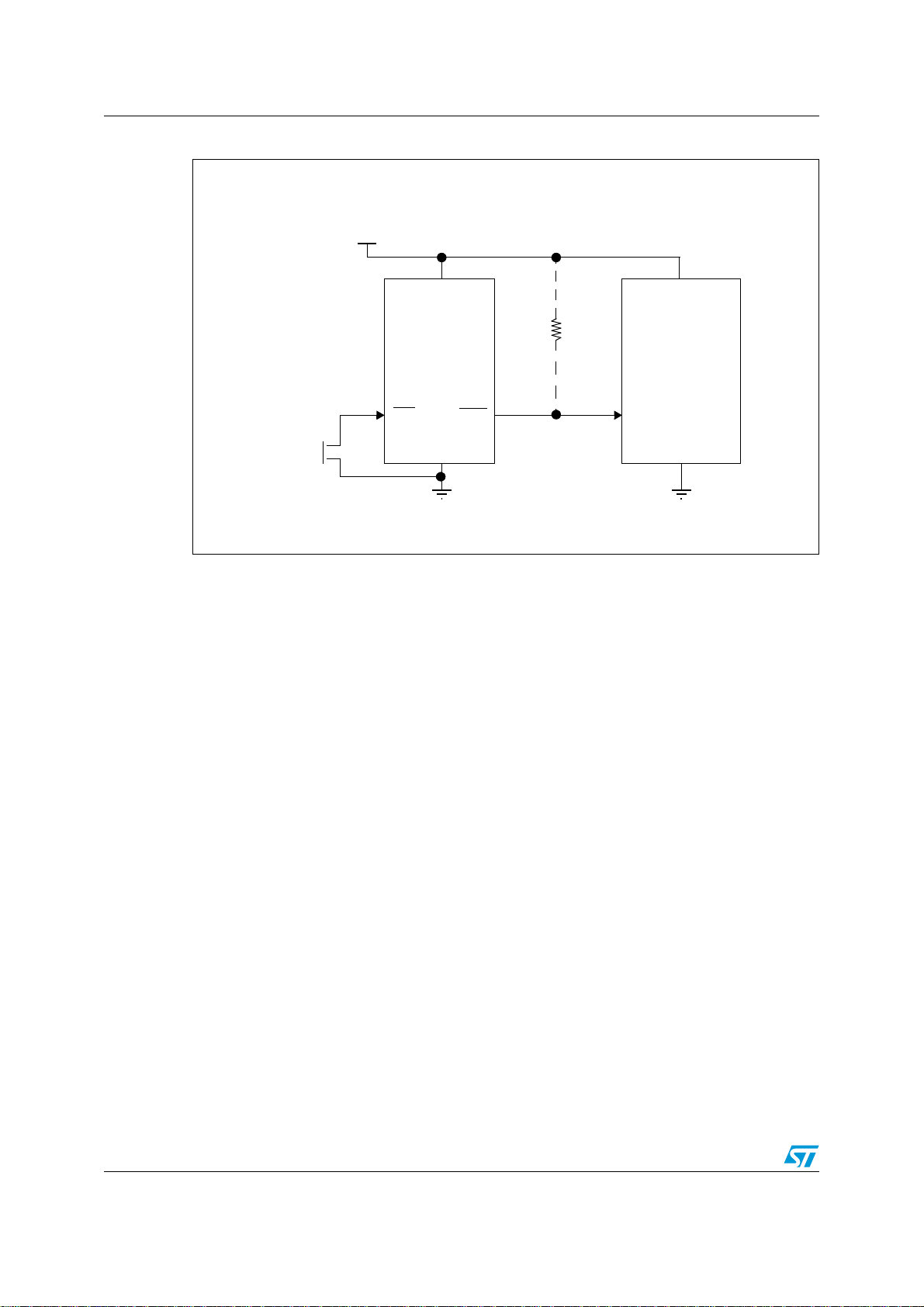
2.4 Reset scheme
Figure 6 shows a typical circuit for controlling the NRST pin operation. The reset input pin
has an internal weak pull-up configured by default exiting from power-on, thus R
omitted. In the case in which an external capacitor is used to filter the NRST external signal,
an external pull-up reduces the charging time of this capacitor.
filtered by
lowpass filter
W
FRST
unknown reset
state
W
NFRST
device under hardware reset
can be
1
‘0
Doc ID 16127 Rev 3 11/27
Page 12
Reset AN3024
Figure 6. Reference reset circuit
V
DD
Manual
Reset
V
DD
Open drain
reset
RST
V
SS
VDD_HV
R
1
SPC560B/C4/5x
NRSTMR
VSS_HV
12/27 Doc ID 16127 Rev 3
Page 13
AN3024 ADC
3 ADC
3.1 Introduction
The device uses a dedicated supply pair VDD_HV_ADC/VSS_HV_ADC for the ADC analog
module so as to decouple the ADC reference voltage from the noise generated either by
another part of the device or by the external application components. VDD_HV_ADC must
be at the same voltage level as the VDD_HV.
There are three different ADC input channels types:
● ANP—internal multiplexed precise channels used for conversion requiring a low TUE
● ANS—internal multiplexed standard channels used for conversion requiring a standard
TUE
● ANX—external multiplexed channels used in conjunction with external multiplexer
controlled directly by the device
ANPs are input only pins. For channel characteristics, please refer to the ADC electrical
characteristics section in the device datasheet (see Section A.1: Reference document).
Figure 7. ADC input scheme
ADC system
Digital
Interface
D
A
Analog
switch
MUX 20
MUX 16
.
.
.
.
.
.
Up to 32 extended channels
through external MUX
MUX 8
3
ANX[3]
ANX[2]
ANX[1]
ANX[0]
ANS[15] (Ch 47)
ANS[0] (Ch 32)
ANP[15] (Ch 15)
ANP[0] (Ch 0)
(Ch 88–95)
MUX 8
MUX 8
MA[2:0]
(Ch 80–87)
Up to 20 channels
medium accuracy
16 channels
high accuracy
MUX 8
(Ch 64–71)
(Ch 72–79)
Doc ID 16127 Rev 3 13/27
Page 14

ADC AN3024
3.2 ADC performances optimization
The equivalent analog input interface of an ADC channel is shown in Figure 8.
Figure 8. Input equivalent circuit
EXTERNAL CIRCUIT INTERNAL CIRCUIT SCHEME
V
DD
Source Filter Current Limiter
Channel
Selection
Sampling
R
S
V
A
RS Source Impedance
R
Filter Resistance
F
Filter Capacitance
C
F
Current Limiter Resistance
R
L
R
Channel Selection Switch Impedance
SW
Sampling Switch Impedance
R
AD
Pin Capacitance (two contributions, CP1 and CP2)
C
P
C
Sampling Capacitance
S
R
F
C
F
R
L
C
P1
R
SW
C
P
R
AD
C
S
To minimize the error induced by the voltage partitioning between this resistance (sampled
voltage on C
) and the sum of RS + RF + RL + RSW + RAD, the external circuit must be
S
designed to respect the Equation 1:
Equation 1
RSRFRLR
+++ +
----------------------------------------------------------------------
V
A
R
EQ
SW
R
AD
1
-- -
<• LSB
2
Please refer to the analog-to-digital converter (ADC) chapter in RM0017 for type
specification versus pins and to the ADC electrical characteristics section in the device
datasheet for parameter values (see Section A.1: Reference document).
14/27 Doc ID 16127 Rev 3
Page 15

AN3024 External oscillators
4 External oscillators
4.1 Introduction
The product offers four clock sources to cover the various types of application:
● Fast internal RC oscillator
● Fast external crystal oscillator
● Slow internal RC oscillator
● Slow external crystal oscillator
An internal PLL is available to optimize the oscillator choice versus the required system
frequency.
This section is focused on the two external oscillators:
● The fast external crystal oscillator for the system clock covering 4 MHz to 16 MHz
● The slow external crystal oscillator for the 32 kHz low power clock
4.2 Fast external crystal oscillator (4 to 16 MHz)
The fast external crystal oscillator must be in the frequency range from 4 MHz to 16 MHz. If
the crystal (resonator) is in the range from 4 MHz to 8 MHz, the oscillator margin can be
adjusted by using an option bit which reduces the fast external crystal oscillator
consumption (low consumption configuration). The default manufacturing oscillator margin
is in the range from 4 MHz to 16 MHz.
Please refer to the RM0017 (see Section A.1: Reference document) for additional
information about option bits and oscillator margin.
To reduce EMC emissions, it is recommended to use the slowest crystal (resonator)
together with the internal PLL, thus achieving the proper system operating frequency. The
drawback of using a slow crystal is the longer start-up time.
Figure 9 shows the external circuit needed for using the oscillator with a crystal or a
resonator.
Figure 9. Reference oscillator circuit
DEVICE
EXTAL
XTAL
Crystal
C1
C2
DEVICE
EXTAL
Resonator
XTAL
For additional information, please refer to the fast external crystal oscillator (4 to 16 MHz)
electrical characteristics section in the device datasheet (see Section A.1: Reference
document).
Doc ID 16127 Rev 3 15/27
Page 16

External oscillators AN3024
4.3 Slow external crystal oscillator (32 kHz)
Figure 10 shows the external circuit needed for using the low power oscillator with a 32 kHz
crystal.
Figure 10. Low power oscillator and resonator connection scheme
OSC32K_EXTAL
Crystal
OSC32K_XTAL
DEVICE
For additional information, please refer to the slow external crystal oscillator (32 kHz)
electrical characteristics section in the device datasheet (see Section A.1: Reference
document).
4.3.1 Some recommended crystal
Ta bl e 2 gives the references of recommended crystals certified by resonators suppliers and
verified through designer simulation in addition to the ones listed in the DS.
T a ble 2. Recomanded crystal
Part number Family name Freq. CL Supplier
EXS00A-MU00265 NX3215SA 32kHz 15pF NDK
1TJF0SPFP1AC00E DST310S 32kHz 15pF KDS
C1
C2
OSC32K_EXTAL
Resonator
OSC32K_XTAL
DEVICE
x
However it is suggested to perform matching directly on customer application board, in order
to verify board parassitics.
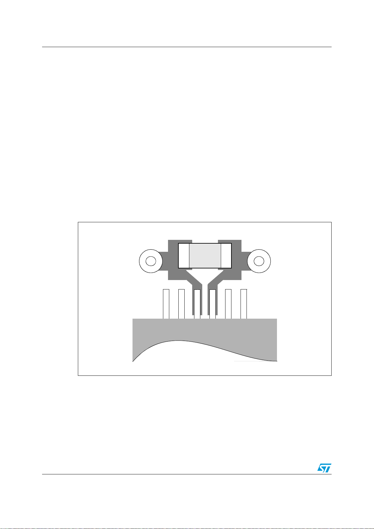
4.4 Layout recommendations
The following recommendations should be observed for designing the oscillator circuitry
layout:
● A current flow at the crystal fundamental frequency runs through the oscillator circuit. If
the oscillator is clipped, then the higher order harmonics are present. To minimize the
emissions generated by these currents, the oscillator circuit should be kept as compact
as possible.
● VSS_HV should be connected directly to GND (V
flow easily between VSS_HV and the two capacitors (C
● Avoid other high frequency signals near the oscillator circuitry.
16/27 Doc ID 16127 Rev 3
island) so that return currents can
SS
and C2).
1
Page 17

AN3024 External oscillators
● Use the same GND for oscillator and oscillator driver (VSS_HV is between EXTAL and
XTAL, V
● Layout: configure the GND supply at low impedance.
● Shield the crystal with an additional ground plane underneath the crystal.
● Do not place sensitive signals near the oscillator. Analyze cross-talk between different
island)
SS
layers.
● The VSS pins close to the XTAL pin must be connected to GND plane (V
island) and
SS
decoupled from the closest VDD pin.
● Capacitors are placed between both ends of the crystal and GND (guard ring). The ring
must be as small as possible.
● If the crystal package is metallic, it should be connected directly to GND.
● For isolating the noise from or to a particular area of the PCB, it is possible to surround
this area with a “guard ring.”
Figure 11 shows an example of an oscillator circuitry layout.
Figure 11. Oscillator circuitry layout
Doc ID 16127 Rev 3 17/27
Page 18
Boot configuration AN3024
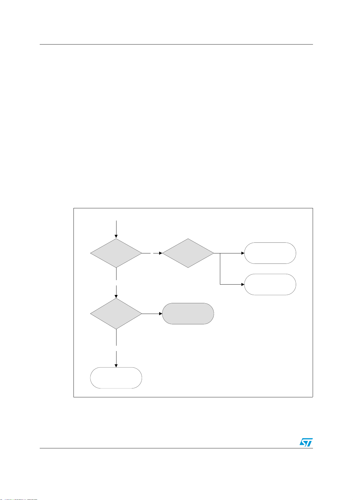
5 Boot configuration
5.1 Introduction
The boot of the device is managed by the boot assist module (BAM).
The following boot modes are supported:
● Single chip (SC)—The device boots from the first bootable section of the Flash main
array.
● Serial boot (SBL)—The device downloads boot code from either LINFlex_0 or
FlexCAN_0 interface and executes it.
The boot mode selection is obtained by setting two pins: FAB and ABS[0].
5.2 Boot mode selection
The device detects the boot mode based on external pins (FAB and ABS[0]) and device
status. Figure 12 shows the boot sequence.
Figure 12. Boot mode selection
0/2
&!"- !"3
.
&LASH"OOT)$
INANYBOOTSECTOR
NO"OOT)$
3TATIC-ODE
9
&LASH"OOTFROM
LOWESTSECTOR
!"3
!"3
3ERIAL"OOT3",
,).&LEX
3ERIAL"OOT3",
&LEX#!.
'!0'2)
In Figure 12, the grey blocks represent hardware-implemented functions, while the white
ones are software-implemented functions in ROM memory.
18/27 Doc ID 16127 Rev 3
Page 19

AN3024 Boot configuration
To boot either from FlexCAN_0 or LINFlex_0, the device must be forced into an alternate
boot loader mode via FAB pin (pad PA[9]). The type of alternate boot mode (CAN or LIN) is
selected according to the ABS[0] pin (pad PA[8]).
FAB and ABS[0] pins must be forced in the required state before initiating the reset
sequence.
.
Table 3. Boot mode selection
FAB
(pad PA[9])
10XLINFlex_0
11XFlexCAN_0
0 X Valid Single chip
0 X Not valid Static mode
In single-chip mode, hardware searches the Flash boot sector for a valid boot ID. As soon as
the device detects a bootable sector, it reads the 32-bit word at offset 0x4 at the detected
sector. Single-chip mode is managed by hardware and BAM is not used.
BAM is executed only in the following cases:
● Serial boot mode has been selected by FAB pin.
● Hardware has not found a valid Boot-ID in any Flash boot locations.
If booting is not possible with the selected configuration (for example, if no Boot ID is found
in the selected boot location) then the device enters the static mode.
Please refer to the boot assist module (BAM) chapter in RM0017 (see Section A.1:
Reference document) for additional information.
5.3 Boot pin scheme
ABS[0]
(pad PA[8])
Boot ID Boot mode
To make all boot configurations possible, it is recommended to use external switches
connected to the FAB and ABS[0] pins, as shown in Figure 13.
Figure 13. Boot mode selection implementation example
6
$$
K:
6
$$
K:
.OTE4HEPINS&!"AND!"3;=HAVETHEBOOTMODESELECTIONFUNCTIONDURINGRESETPHASE!FTERRESETPHASE
EYARENORMAL)/PINSANDCANBEUSEDACCORDINGTOAPPLICATIONNEEDS
TH
Doc ID 16127 Rev 3 19/27
30#"#X
&!"
!"3;=
'!0'2)
Page 20

Debug AN3024
6 Debug
6.1 Introduction
The device features JTAG and Nexus 2+ interfaces.
The Nexus 2+ interface is available only on the LBGA208 development package and is not
discussed in this document. Nexus 2+ pins are located on dedicated pads.
6.2 JTAG I/Os
The JTAG interface is composed of:
● Test data input (TDI) on pin PC[0]
● Test data output (TDO) on pin PC[1]
● Test mode select (TMS) on pin PH[10]
● Test clock input (TCK) on pin PH[9]
Out of reset, all JTAG signals are configured for the JTAG communication. They can be
configured by software as user I/Os and made available to the application. If the application
needs to combine both the JTAG functionality for debug and programming purposes
together with the standard I/O function, some limitations must be considered:
● PC[0], PC[1], PH[9] and PH[10] cannot be debugged using a JTAG debug interface.
● The configuration of PC[0], PC[1], PH[9] or PH[10] as user I/Os prevents the
communication with the debugger, making impossible to debug the application.
● These pins can only be set back to the JTAG functionality by means of a hardware or
software reset (it cannot be done through the JTAG debugger).
An external hardware application connected to those signals might interfere with JTAG
signals, making it impossible to enter debug mode without disconnecting the external
hardware. It is preferable to use these JTAG pins to define the hardware configuration of the
application rather than critical application functions.
6.3 JTAG connector scheme
Figure 14. JTAG connector scheme
6
$$
0#;=4$)
;=4$/
0#
;=4#+
0(
.234
K:
0(;=4-3
K:
'!0'2)
20/27 Doc ID 16127 Rev 3
Page 21

AN3024 I/Os
7 I/Os
7.1 Introduction
The device features a unique pad technology to sustain a current injection of ± 5 mA on
digital and analog inputs. A simple serial resistor is sufficient to protect the input
characteristics.
7.2 I/O types
The device features three I/O types with different drive strength:
● SLOW type—This is the most common output type suitable for most of the application
output signals and ensuring low electromagnetic emission.
It allows to drive up to 2 mA and can sustain a maximum frequency of 2 MHz.
● MEDIUM type—This output type can sustain a higher frequency with a reduced delay
to meet the requirements of SPI communication or high speed CAN communication.
It allows to drive up to 3.8 mA and can sustain a maximum frequency of 16 MHz.
Out of reset, the medium speed outputs are configured as slow. To obtain the medium
performance the application must configure the slew rate using the SRC field in the
corresponding SIUL pad configuration register (SIUL_PCR).
● FAST type—Only the Nexus MCKO signal features a fast pad which is not a user
signal.
Maximum output frequency depends directly on the capacitive load connected on the
output.
Please refer to the device datasheet and RM0017 (see Section A.1: Reference document),
for the detailed electrical characteristics and port mapping.
Note: 1 All output types have a slope control (current) to reduce the EMI.
2 TDO pad is medium speed only. Writing the SRC field in the corresponding SIUL_PCR has
no effect.
7.3 I/Os configuration after reset
To avoid activating external components while under reset, all pads are forced to
high impedance inputs, with the following exceptions:
● RESET is driven low
● Boot mode pins
–FAB is pull-down
– ABS[0] is pull-up
● JTAG pins
– TCK, TMS and TDI are pull-up
– TDO is high impedance
Doc ID 16127 Rev 3 21/27
Page 22

I/Os AN3024
7.4 Maximum output current
The application must not modify the maximum current drive expected on each I/O type and
I/O segment. An I/O segment is a group of pads supplied by the same V
Table 4. I/O supply segment
Supply segment
Package
123456
LBGA208
LQFP144 pin20–pin49 pin51–pin99 pin100–pin122 pin123–pin19 — —
(1)
Equivalent to LQFP144 segment pad distribution MCKO MDOn/MSEO
DD_HV/VSS_HV
pair.
LQFP100 pin16–pin35 pin37–pin69 pin70–pin83 pin84–pin15
1. LBGA208 available only as development package for Nexus2+.
In order to keep the maximum current on each segment in specification, both static and
dynamic consumptions must be considered:
● The maximum static current must remain below maximum I
ensure device reliability. The parameter I
AVG SEG
represents the average current drawn
by all outputs belonging to the same segment. For example, if V
I
AVG SEG
● The maximum dynamic current must remain below maximum I
ensure the device functionality. The parameter I
=70mA.
DYNSEG
dynamic and static current drawn by all outputs belonging to the same segment. For
example, if V
= 5 V then I
DD
DYNSEG
=110mA.
Please refer to the I/O pad current specification section in the device datasheet and
RM0017 (see Section A.1: Reference document) for the detailed electrical characteristics
and port mapping.
The dynamic consumption is caused by the output driver transistors during the output switch
and therefore is present only during the transition phase of the output (rising or falling edge).
For example, if the maximum dynamic consumption of a SLOW type output is 20 mA, the
transition lasts for 50 ns. Moreover, supposing that there is no static consumption on this I/O
segment a maximum of five slow type outputs can switch simultaneously (in this case,
50 ns) in order to respect the maximum I
DYNSEG
expected value, I
If a static current is drawn from the same segment, the dynamic consumption must be
reduced accordingly. For example, if 16 outputs of the same segment draw out a total static
current equal to 25 mA, the maximum dynamic consumption is reduced to 85 mA.
— —
AVG SEG
value so as to
= 5 V then
DD
DYNSEG
value so as to
represents the sum of the
DYNSEG
= 110 mA.
7.5 I/O characteristic in STANDBY mode
In STANDBY mode the I/Os are disconnected from supply and they are in high impedance
state. Only the wake-up lines can be configured as:
● High-impedance input (default configuration)
● Input with weak pull-up
The configuration of the wake-up lines is supported in the wake-up unit. Please refer to the
wakeup unit (WKPU) chapter in RM0017 (see Section A.1: Reference document) for
additional information.
22/27 Doc ID 16127 Rev 3
Page 23

AN3024 I/Os
Note: All wake-up lines left floating cause additional consumption due to their Schmitt Trigger
logic. To avoid unnecessary consumption all wake-up lines should be kept to V
or VDD
SS
either by the application or using the internal weak pull-up.
The TDO pad is part of the STANDBY domain in order to provide a handshaking mechanism
with a debugger in STANDBY mode. However, in STANDBY mode the TDO pin is configured
as input without pull-resistor and as a consequence, when no debugger is connected, the
TDO pad is floating causing additional current consumption.
In order to avoid additional consumption, TDO must be tied to V
external pull-up (or pull-down) resistor in the range of 47–100 kΩ.
If the PA[1] pin is configured as NMI the pull-up is automatically activated, but this has no
effect during STANDBY mode. In this case pull-up is then correctly configured through the
WKPU_WIPUER register; no external resistor is necessary.
7.6 General consideration for I/O
To avoid excess consumption and to improve the reliability of the application it is
recommended to configure unused I/Os as input with pull-up.
During the application design the absolute maximum voltage on I/O must be considered:
● respect to ground: +6 V
● respect to V
V
+ 0.3
DD
For more details refer to the device datasheet (see Section A.1: Reference document).
: Voltage of each pin must remain in the range from VDD − 0.3 and
DD
or GND by means of an
DD
Doc ID 16127 Rev 3 23/27
Page 24

EMC guidelines AN3024
8 EMC guidelines
This section summarizes recommendations for the system designers to improve the EMC
(electromagnetic compatibility) and, in particular, to reduce the radiant emissions of a
system based on the SPC560Bxx and SPC560Cxx devices.
Obviously, not all EMC techniques are covered. Therefore, it is recommended to refer to
other, more general EMC documentation in parallel to the present application note.
8.1 SPC560Bxx/Cxx software configurations
The SPC560Bxx/Cxx family offers some features that allow, with software configurations, to
cover some requests for reduction in the electromagnetic interference (or EMI) emissions:
● The system clock should be chosen to avoid overlapping with known frequency (bands
of interest)
● The FMPLL gives the possibility to modulate the system clock so to reduce the picks of
emission.
● Choose the lowest possible slew rate of pins accordantly with the functionality choose
for the pins
● The peripherals that are not used in the application should be disabled and clock gated
● Configuring the unused pins as input weak pull-up (default configuration)
8.2 Hardware guidelines
Some recommendations to design a system layout are listed below:
● V
● Fast external crystal oscillator
decoupling capacitors
DD
Decoupling capacitors must be used to decouple BV and all HV and ADC supply pins
from GND. To avoid that the decoupling capacitors’ parasitic inductance couples with
the capacitance plane of the supply planes, certain measures of precaution should be
taken:
– Place the capacitors as close as possible to the V
device.
– Use power planes or wide traces to connect from the SPC560Bxx/Cxx device to
the capacitor.
– Use as many vias as possible in the connections from the SPC560Bxx/Cxx device
to the capacitors. For example, use at least two vias to connect the positive side of
the capacitor to the power plane.
To reduce EMC emissions, it is recommended to use the slowest crystal (resonator)
together with the internal PLL, thus achieving the proper system operating frequency.
The drawback of using a slow crystal is the longer startup time. In order to minimize the
amount of emissions, generated from the currents flowing in the oscillator circuit at the
crystal's fundamental frequency, the oscillator circuit should be kept as compact as
possible.
pins on the SPC560Bxx/Cxx
DD
24/27 Doc ID 16127 Rev 3
Page 25

AN3024 EMC guidelines
● Grounding
Usually in a system it is possible identify different parts of circuits including digital,
analog, high current switching circuitry, I/O, and the main power supply. If these
different parts of the circuit use isolated grounds, they will be connected together at a
single point.
● PCB considerations:
– For single-chip applications, a minimum of four layers is used. For expanded mode
applications, a minimum of six layers is used.
– There is at least one ground plane.
– There is at least one power plane.
– From the power and ground planes have not be present structures which obstruct
the flow of current, such as via overlapping (it is not allowed three via anti-pads to
merged). Furthermore, vias should be staggered as much as possible because
aligned vias create slots that obstruct the flow of current.
Doc ID 16127 Rev 3 25/27
Page 26

26/27 Doc ID 16127 Rev 3
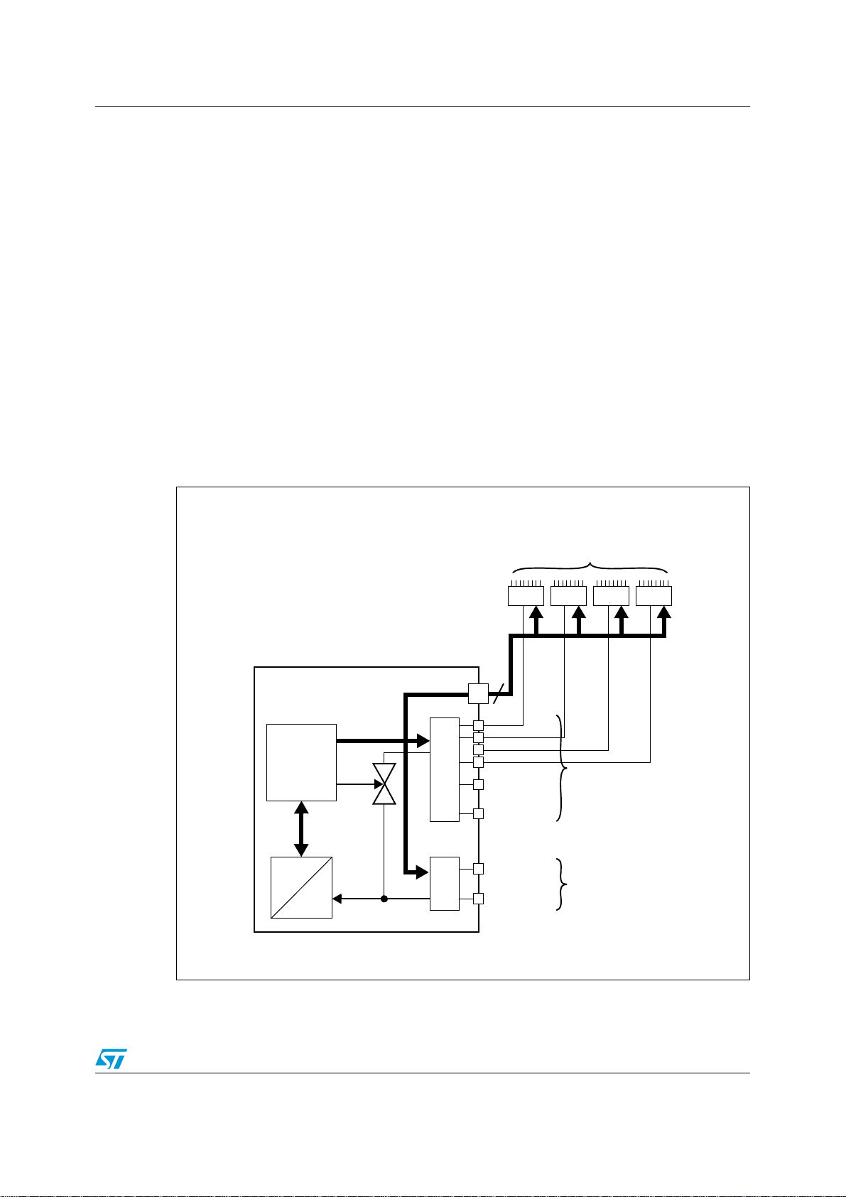
9 Reference schematic
Figure 15 shows a typical application schematic.
Figure 15. Typical application schematic
Reference schematic AN3024
GAPGRI00208
Page 27

AN3024 Document management
Appendix A Document management
A.1 Reference documents
● SPC560B4x, SPC560B5x, SPC560C4x, SPC560C5x 32-bit MCU family built on the
embedded Power Architecture
● 32-bit MCU family built on the Power Architecture
body electronics applications (SPC560B4x, SPC560B5x, SPC560C4x, SPC560C5x
datasheet, Doc ID 14619)
● 32-bit MCU family built on the Power Architecture
body electronics applications (SPC560B4x/50 – SPC560C4x/50 errata sheet,
Doc ID 15844)
A.2 Acronyms
Table 5. Acronyms
Acronym Name
ADC Analog-to-digital converter
BAM Boot assist mode
CRC Cyclic redundancy check
EMC Electromagnetic compatibility
EMI Electromagnetic interference
ESL Equivalent series inductance
ESR Equivalent series resistance
®
(reference manual RM0017, Doc ID 14629)
®
embedded category for automotive
®
embedded category for automotive
LVD Low voltage detector
NVUSRO Non-volatile user options register
POR Power-on reset
SIUL System integration unit lite
TCK Test clock input
TDI Test data input
TDO Test data output
TMS Test mode select
Doc ID 16127 Rev 3 27/27
Page 28
Revision history AN3024
Revision history
Table 6. Document revision history
Date Revision Changes
22-Sep-2009 1 Initial release.
Editorial and formatting changes throughout document
Updated Section 1.3: Current consumption and voltage regulator
03-Sep-2010 2
04-Jun-2012 3 Added Section 4.3.1: Some recommended crystal.
and Section 7.5: I/O characteristic in STANDBY mode
Added Section 8: EMC guidelines
Updated Table 5: Acronyms
28/27 Doc ID 16127 Rev 3
Page 29

AN3024
U
D
W
D
W
S
O
U
T
R
G
A
Y,
D
E
G
Please Read Carefully:
Information in this document is provided solely in connection with ST products. STMicroelectronics NV and its subsidiaries (“ST”) reserve the
right to make changes, corrections, modifications or improvements, to this document, and the products and services described herein at any
time, without notice.
All ST products are sold pursuant to ST’s terms and conditions of sale.
Purchasers are solely responsible for the choice, selection and use of the ST products and services described herein, and ST assumes no
liability whatsoever relating to the choice, selection or use of the ST products and services described herein.
No license, express or implied, by estoppel or otherwise, to any intellectual property rights is granted under this document. If any part of this
document refers to any third party products or services it shall not be deemed a license grant by ST for the use of such third party products
or services, or any intellectual property contained therein or considered as a warranty covering the use in any manner whatsoever of such
third party products or services or any intellectual property contained therein.
NLESS OTHERWISE SET FORTH IN ST’S TERMS AND CONDITIONS OF SALE ST DISCLAIMS ANY EXPRESS OR IMPLIE
ARRANTY WITH RESPECT TO THE USE AND/OR SALE OF ST PRODUCTS INCLUDING WITHOUT LIMITATION IMPLIE
ARRANTIES OF MERCHANTABILITY, FITNESS FOR A PARTICULAR PURPOSE (AND THEIR EQUIVALENTS UNDER THE LAW
F ANY JURISDICTION), OR INFRINGEMENT OF ANY PATENT, COPYRIGHT OR OTHER INTELLECTUAL PROPERTY RIGHT.
NLESS EXPRESSLY APPROVED IN WRITING BY TWO AUTHORIZED ST REPRESENTATIVES, ST PRODUCTS ARE NO
ECOMMENDED, AUTHORIZED OR WARRANTED FOR USE IN MILITARY, AIR CRAFT, SPACE, LIFE SAVING, OR LIFE SUSTAININ
PPLICATIONS, NOR IN PRODUCTS OR SYSTEMS WHERE FAI LURE OR MALFUNCTION MAY RESULT IN PERSONAL INJUR
EATH, OR SEVERE PROPERTY OR ENVIRONMENTAL DAMAGE. ST PRODUCTS WHICH ARE NOT SPECIFIED AS "AUTOMOTIV
RADE" MAY ONLY BE USED IN AUTOMOTIVE APPLICATIONS AT USER’S OWN RISK.
Resale of ST products with provisions different from the statements and/or technical features set forth in this document shall immediately void
any warranty granted by ST for the ST product or service described herein and shall not create or extend in any manner whatsoever, any
liability of ST.
The ST logo is a registered trademark of STMicroelectronics. All other names are the property of their respective owners.
ST and the ST logo are trademarks or registered trademarks of ST in various countries.
Information in this document supersedes and replaces all information previously supplied.
© 2012 STMicroelectronics - All rights reserved
STMicroelectronics group of companies
Australia - Belgium - Brazil - Canada - China - Czech Republic - Finland - France - Germany - Hong Kong - India - Israel - Italy - Japan -
Malaysia - Malta - Morocco - Philippines - Singapore - Spain - Sweden - Switzerland - United Kingdom - United States of America
www.st.com
Doc ID 16127 Rev 3 27/27
 Loading...