


AN3023
Application note
Using the analog-to-digital converter of the STM8A microcontroller
Introduction
The purpose of this application note is to explain how to use the analog-to-digital converter
implemented in the STM8A microcontroller family. The document provides useful
information on how to configure the ADC registers and microcontroller resources and use
the analog-to-digital converter in different modes.
The STM8A firmware library, containing source code of all the examples described in this
application note, can be downloaded from the STMicroelectronics website: www.st.com.
October 2009 Doc ID 16113 Rev 1 1/23
www.st.com

Contents AN3023
Contents
1 ADC hardware description . . . . . . . . . . . . . . . . . . . . . . . . . . . . . . . . . . . . 3
1.1 General properties . . . . . . . . . . . . . . . . . . . . . . . . . . . . . . . . . . . . . . . . . . . 3
1.2 ADC operation . . . . . . . . . . . . . . . . . . . . . . . . . . . . . . . . . . . . . . . . . . . . . . 5
2 Summary of the features . . . . . . . . . . . . . . . . . . . . . . . . . . . . . . . . . . . . . 7
3 Configuring ADC registers for conversion . . . . . . . . . . . . . . . . . . . . . . . 9
3.1 ADC setup . . . . . . . . . . . . . . . . . . . . . . . . . . . . . . . . . . . . . . . . . . . . . . . . . 9
3.1.1 ADC clock . . . . . . . . . . . . . . . . . . . . . . . . . . . . . . . . . . . . . . . . . . . . . . . . 9
3.1.2 ADC on/off control (power on) . . . . . . . . . . . . . . . . . . . . . . . . . . . . . . . . . 9
3.1.3 Channel selection . . . . . . . . . . . . . . . . . . . . . . . . . . . . . . . . . . . . . . . . . 10
3.1.4 Conversion on external trigger . . . . . . . . . . . . . . . . . . . . . . . . . . . . . . . . 10
3.1.5 Conversion modes . . . . . . . . . . . . . . . . . . . . . . . . . . . . . . . . . . . . . . . . . 10
3.2 Storing converted values . . . . . . . . . . . . . . . . . . . . . . . . . . . . . . . . . . . . . 17
3.3 ADC interrupt management . . . . . . . . . . . . . . . . . . . . . . . . . . . . . . . . . . . 17
4 Practical application . . . . . . . . . . . . . . . . . . . . . . . . . . . . . . . . . . . . . . . . 18
4.1 Areas of use . . . . . . . . . . . . . . . . . . . . . . . . . . . . . . . . . . . . . . . . . . . . . . . 18
4.2 Hardware connection examples . . . . . . . . . . . . . . . . . . . . . . . . . . . . . . . . 18
4.3 Methods for precision improvement . . . . . . . . . . . . . . . . . . . . . . . . . . . . . 20
5 Design recommendations . . . . . . . . . . . . . . . . . . . . . . . . . . . . . . . . . . . 21
6 Revision history . . . . . . . . . . . . . . . . . . . . . . . . . . . . . . . . . . . . . . . . . . . 22
2/23 Doc ID 16113 Rev 1

AN3023 ADC hardware description
1 ADC hardware description
1.1 General properties
STM8A family microcontrollers include an analog-to-digital converter which has up to 16
multiplexed inputs. The ADC resolution is 10 bits. The number of external analog inputs
depends on the package size of the particular STM8A family device.
The ADC is a successive approximation analog-to-digital converter. Conversion can be
performed in continuous mode or single mode. The digital result is then stored in registers.
Because the ADC resolution is 10 bits and the ADC data register length is 16 bits, the
analog-to-digital converter result is stored in two 8-bit registers, and the data is either right
or left aligned (this is selectable).
The event used to start conversion can be generated by software or by the STM8A
microcontroller's internal timer 1 and timer 2
(a)
(any type of timer event can be used). The
start of A/D conversion can also be triggered by an external pin.
The reference voltage for the analog-to-digital converter depends on the package. It comes
either from an external source—in this case the reference must be connected to two
external pins—or is connected internally to analog power supply pins. The value of this
reference voltage is limited to within the range from 2.75 V up to the voltage applied on the
V
input. The measured voltage must be between V
DDA
REF+
and V
. Resolution can be
REF−
increased by so-called analog zooming—using a smaller reference voltage around the
range of values to be measured.
If needed, an interrupt can be generated at the end of conversion and if an analog watchdog
event occurred.
The analog-to-digital converter is driven by a clock derived from the MCU master clock
through a programmable divider. This allows you to select the ADC clock speed according to
your application requirements.
a. Trigger feature available on selected devices
Doc ID 16113 Rev 1 3/23
ADC hardware description AN3023
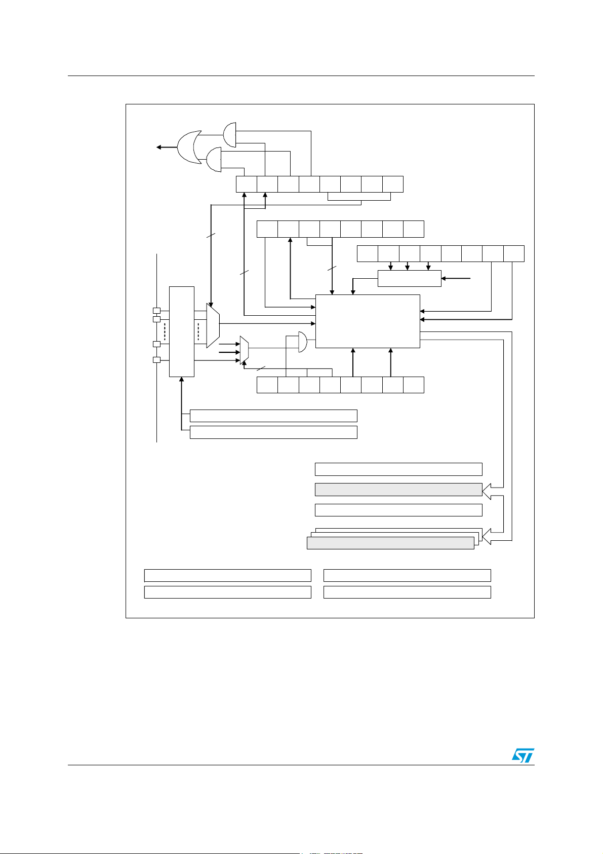
Figure 1. ADC block diagram
Interrupt
AIN0
AIN1
AIN15
ADC_ETR
Genera l
Purpose
IOs
EOC AWD CH3 CH2 CH 1 CH0
4
2
Mux
TIM1
TIM2
Schmitt Trigger Enable TE[7:0]
Schmitt T rigger Enable TE [15:8]
EOCIE
DBUF OVR
2
EXT
TRIG
AWDIE
ADON
ADON
SyncE
Sync
2
Analog-to-Digital
EXT
EXT
SEL1
SEL0
- - - -
SP
SEL2SPSEL1SPSEL0
CK_ADC f
Prescaler
/2, /3 : /1 8
Converter
ALIGN - SCAN -
AWDG voltage reference low
- - CON T ADON
MASTER
AWDG Status Register chan nel [7 :0]
AWDG S tatus Register channel [15 :8]
1. Refer to STM8A reference manual for ADC registers bit description
4/23 Doc ID 16113 Rev 1
Data Re gist er
AWDG voltage refere nce high
Data Bu ffer
AWDG Enable Register ch annel [7 :0]
AWDG E nable Register channel [15:8]
AN3023 ADC hardware description
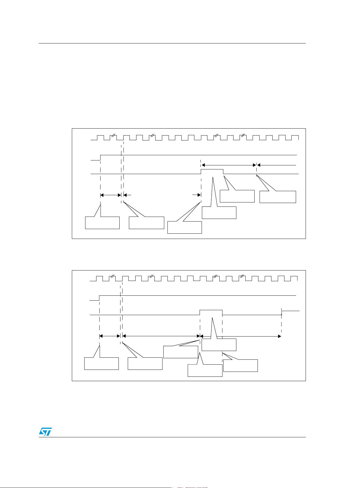
1.2 ADC operation
The analog-to-digital converter supports two basic conversion modes: single mode and
continuous mode.
Figure 2 and Figure 3 describe single and continuous mode analog-to-digital converter
operation.
In single conversion mode, the analog-to-digital converter performs only one conversion on
the selected channel.
Figure 2. Single conversion mode
CLK
ADON
EOC
Power-on ADC
ADON=1
t
STAB
conversion time (14 clocks)
1 sync clock
3 clocks sampling time
10 clocks conversion
Start conversion
ADON=1 or trigger
ADC inactive
Software clears
EOC bit
Software reads
ADC data
End of conversion
next conversion
Start conversion
ADON=1 or trigger
In continuous conversion mode, the analog-to-digital converter starts another conversion as
soon as the previous one is concluded.
Figure 3. Continuous conversion mode
CLK
ADON
EOC
t
STAB
Power-on ADC
ADON=1
conversion time (14 clocks)
Start conversion
ADON=1 or trigger
End of conversion
Next conversion
starts immediately
next conversion time (14 clocks)
Software reads
ADC data
Software clears
EOC bit
As shown in these figures, after ADC power on, the analog-to-digital converter needs a
stabilization time t
(equivalent to one conversion time t
STAB
) before it starts converting
CONV
accurately. For subsequent conversions there is no stabilization delay and ADON needs to
be set only once.
Doc ID 16113 Rev 1 5/23
ADC hardware description AN3023
The ADC conversion time takes 14 clock cycles. In addition to the basic conversion modes,
some packages have extended features for scan mode and buffered continuous mode.
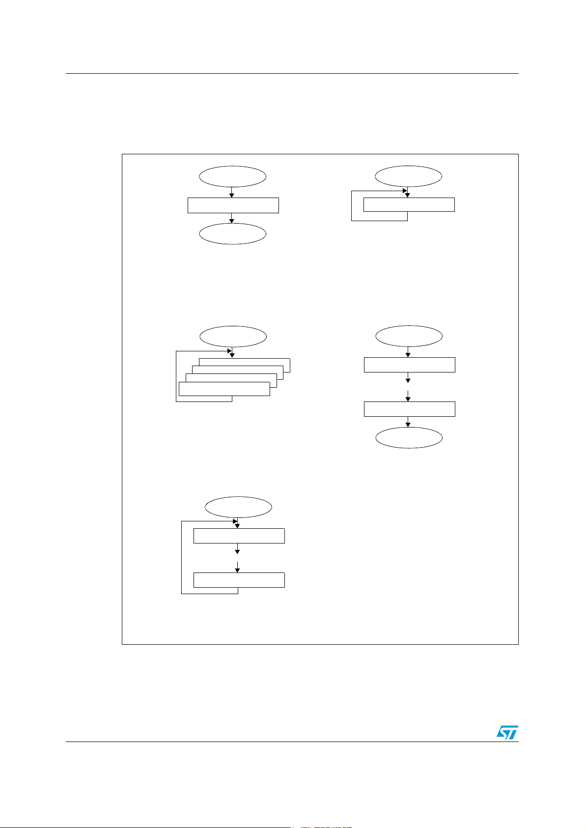
Figure 4 summarizes all the possible analog-to-digital converter operating modes.
Figure 4. ADC operating modes
Start
Channel X conversion
Stop
Single channel
Single conversion
Start
Channel X conversion
Channel X conversion
Channel X conversion
Channel X conversion
Single channel
Continuous and
Buffered conversion
Start
Channel X conversion
Single channel
Continuous conversion
Start
Channel 1 conversion
...
Channel n conversion
Stop
Start
Channel 1 conversion
...
Channel n conversion
Multiple channel
Continuous and
Scan conversion (buffered)
6/23 Doc ID 16113 Rev 1
Multiple channels
Scan conversion (buffered)
AN3023 Summary of the features
2 Summary of the features
The STM8A family contains two types of analog-to-digital converter which are named ADC
and ADC2. Depending on the device, it may contain both (ADC and ADC2) or only one
(ADC).
There are two variants of the first analog-to-digital converter ADC:
1. With standard features
2. With extended features for scan mode, buffered continuous mode and analog
watchdog
The second analog-to-digital converter, ADC2, contains a features subset of the first ADC
module.
Refer to the STM8A datasheet for more information on the available features.
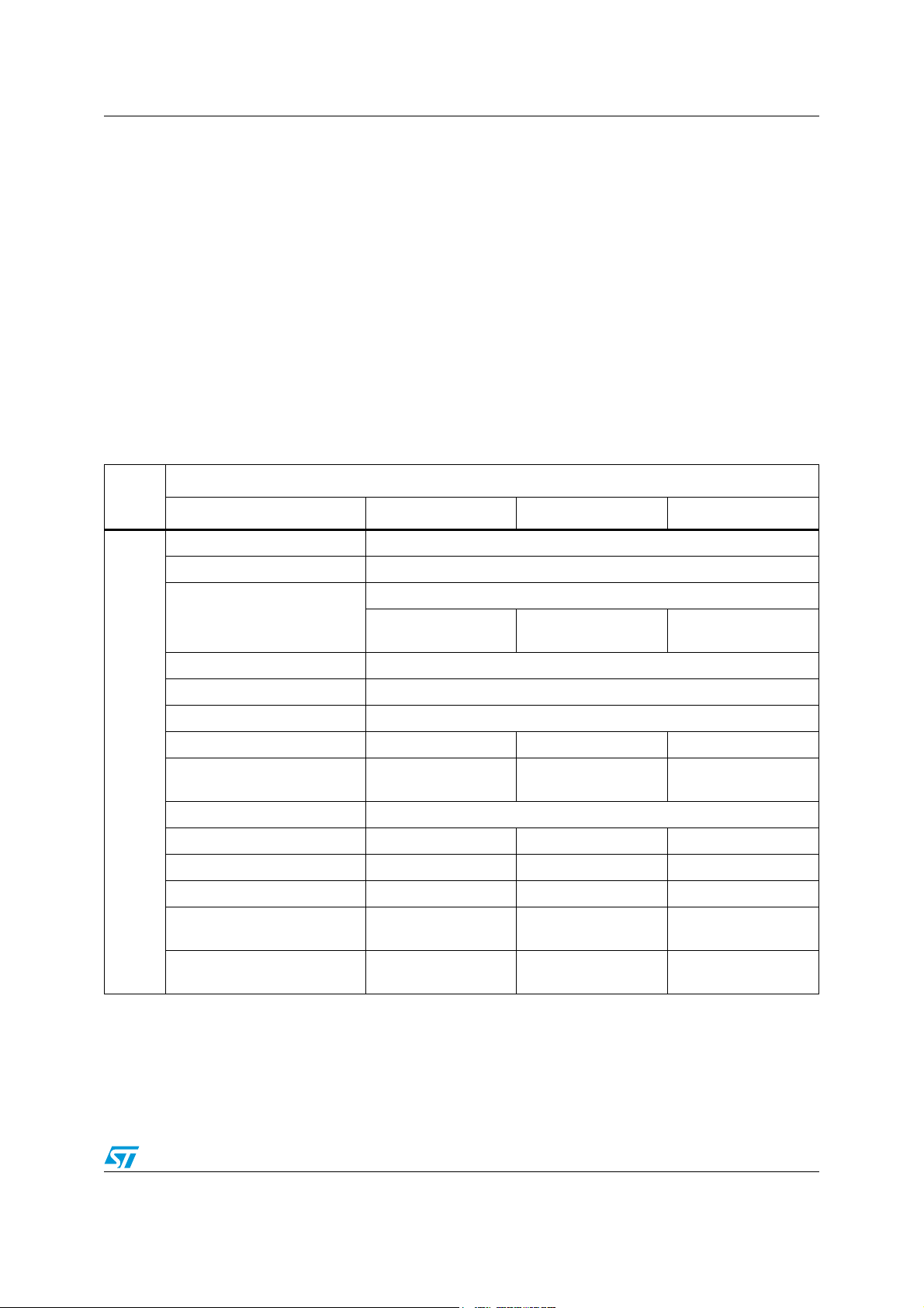
Table 1. ADC and ADC2 features on different devices
Features
Module
Parameter 32 KB die based
Resolution 10-bit
(1)
(2)
128 KB die based
(2)
256 KB die based
(2)
ADC
Programmable prescaler f
MASTER
divided by 2 to 18
Single or continuous mode
Operating modes
Clock speed f
ADC input range V
Conversion speed min. 3.5 µs @ 4 MHz f
Scan and buffered
continuous mode
—
= 1 to 4 MHz
ADC
= V
SSA
IN
= V
Scan and buffered
continuous mode
DDA
ADC
Number of input channels up to 10 up to 16 up to 16
Triggers
Timer 1 and external
ADC_ETR pin
External ADC_ETR
pin
Timer 1, Timer 2 and
external ADC_ETR pin
Data format left or right alignment
ADC interrupt EOC and AWD EOC EOC and AWD
Analog watchdog Yes — Yes
Schmitt trigger enable/disable Yes Yes Yes
Synchronization mechanism
between ADC and ADC2
Analog zooming —
——Yes
Through dedicated
VREF pins
Through dedicated
VREF pins
Doc ID 16113 Rev 1 7/23

Summary of the features AN3023
Table 1. ADC and ADC2 features on different devices
Features
Module
ADC2
Parameter 32 KB die based
Resolution
— — 10-bit
Programmable prescaler — —
Operating modes — —
Clock speed
ADC input range
— —f
— —V
Conversion speed — —
Number of input channels — —12
Triggers
Data format
ADC interrupt
Analog watchdog
Schmitt trigger enable/disable
— — Timer1 and Timer2
— — left or right alignment
— — EOC and AWD
— —Yes
— —Yes
(2)
(1)
(continued)
128 KB die based
(2)
256 KB die based
f
MASTER
divided by 2 to 18
Single or continuous
= 1 to 4 MHz
ADC
= VIN = V
SSA
min. 3.5 µs
@ 4 MHz f
(2)
mode
DDA
ADC
Synchronization mechanism
between ADC and ADC2
— —Yes
Analog zooming — ——
1. For feature details, refer to the STM8A reference manual and the device datasheet.
2. Die information is stored in Chip ID registers. Refer to the reference manual for further details.
8/23 Doc ID 16113 Rev 1

AN3023 Configuring ADC registers for conversion
3 Configuring ADC registers for conversion
3.1 ADC setup
Before starting an ADC conversion, ADC setup is done using the following steps:
● ADC clock selection (define conversion speed)
● Channel selection
● Power on the ADC (set ADON bit)
● Wait for 14 ADC clock cycles (14 * t
● Conversion mode selection (single or continuous)
● Trigger source selection and only after trigger enable
● Apply trigger source or set ADON bit
3.1.1 ADC clock
ADC
)
The clock supplied to the ADC peripheral is the prescaled f
MASTER
applied on bit SPSEL[2:0] in the ADC_CR1 register and it can be selected from f
f
MASTER
/18.
clock. The prescaler is
MASTER
/2 to
The prescaler selection must ensure a maximum 4 MHz ADC frequency.
ADC conversion time depends on the ADC clock frequency, the sampling time duration and
the ADC resolution. The minimum ADC conversion time is 3.5 µs @ 4 MHz ADC clock
frequency.
Note: It is recommended to change bits SPSEL[2:0] when the ADC is in power-down mode. This
is because, internally, there may be a glitch in the clock during this change. If this change is
made when ADC is not in power-down, the user is required to ignore the first converted
result.
3.1.2 ADC on/off control (power on)
The ADC can be powered on by setting the ADON bit in the ADC_CR1 register. When the
ADON bit is set for the first time, it wakes up the ADC from power-down mode.
After power ON, wait for stabilization time and then, to start a conversion, either set the
ADON bit again in the ADC_CR1 register or use an external trigger source (timers or
ADC_ETR pin).
At the end of conversion, the ADC remains powered on and the ADON bit has to be set only
once to start the next conversion. If the ADC is not used for a long time, it is recommended
to switch it off to decrease power consumption. This is done by clearing the ADON bit.
When the ADC is powered on, the output stage of the selected channel is disabled;
therefore it is recommended to select the channel first before powering on the ADC.
Note: If any bit of the ADC_CR1 register other than ADON is changed at the same time, the
conversion is not triggered. This is to prevent triggering an erroneous conversion.
Moreover, be aware that any bit manipulation instruction on the ADC_CR1 register can start
a new conversion due to the fact that the ADON bit is read as ‘1’ and then written back as ‘1’
by this operation.
Doc ID 16113 Rev 1 9/23

Configuring ADC registers for conversion AN3023
3.1.3 Channel selection
There are up to 16 input channels in ADC and up to 12 input channels in ADC2 (the
maximum number of channels per ADC peripheral depends on the MCU package size).
External input channels can be selected by bits CH[3:0] in the ADC_CSR register. If the
channel is changed during an ongoing conversion, the current conversion is reset and a new
start pulse is sent to ADC.
3.1.4 Conversion on external trigger
Conversion can also be started by an external trigger event after ADC power ON.
The external trigger source can be a timer
ADC_ETR
(b)
pin. Bit EXTTRIG is set in the ADC_CR2 register to enable the conversion by
external trigger and the bits EXTSEL[1:0] select the trigger source as either the timer or the
external trigger pin.
The different software sequences (shown below) to select the trigger source and enable the
external trigger depend on the ADC state (powered-ON or powered-OFF).
Case 1: ADC is in powered-ON state
ADC_CR2 = value1; Select the source (EXTSEL[1:0] bits)
ADC_CR2 |= 0x40; Enable external trigger (EXTTRIG bit)
(b)
TRGO event or a rising edge on the external
Case 2: ADC is in powered-OFF state
When the ADC is in powered-OFF state, the user is free to choose between the above
software sequence, that is, for ADC powered-ON state or the sequence below:
ADC_CR2 = value; Select the source and enable the external trigger
3.1.5 Conversion modes
Single conversion mode
In single conversion mode, the ADC performs one conversion on the channel selected by
bits CH[3:0] in the ADC_CSR register. At the end of conversion, the EOC bit is set and the
result can be read from the registers ADC_DRH and ADC_DRL. The interrupt is generated
if the EOC interrupt is enabled in the ADC_CSR register.
Example 1
● f
MASTER
● f
ADC
● Channel = AIN1
● Single conversion mode, left alignment mode
● Starting ADC by software
= 16 MHz
= 4 MHz
b. Refer to the datasheet for the details on the trigger source available.
10/23 Doc ID 16113 Rev 1

AN3023 Configuring ADC registers for conversion
For Example 1, the ADC registers should be configured as follows:
ADC_CR1:SPSEL[2:0] = 010
ADC_CSR:CH[3:0] = 0001
ADC_CR1:ADON = 1
Wait (14/f
ADC_CR1:CONT = 0
Note: Do not perform the operation “ADC_CR1:CONT = 0
CONT bit is already 0 (see note in Section 3.1.2).
ADC_CR2:ALIGN = 0
ADC_CR1:ADON = 1
Wait (ADC_CSR:EOC = 1)
See the result of the conversion in ADC data registers ADC_DRH and ADC_DRL.
) → stabilization time before starting the conversion
ADC
→ ADC power on
→ single conversion mode
→ left alignment
→ starting the conversion by software
→ f
= 4 MHz (that is, f
ADC
→ AIN1 channel selected
→ end of conversion
Continuous conversion mode
In continuous conversion mode, the ADC starts another conversion as soon as it finishes
the last one. A new conversion starts automatically. For this conversion mode, set the CONT
bit to ‘1’ in the ADC_CR1 register.
Example 2
● f
MASTER
● f
ADC
● Channel = AIN2
● Continuous conversion model, right alignment
● Starting ADC by external trigger event on ADC_ETR pin
= 4 MHz
= 1 MHz
MASTER
/4)
→ single conversion mode” if the
For Example 2, the ADC registers should be configured as follows:
ADC_CR1:SPSEL[2:0] = 010
ADC_CSR:CH[3:0] = 0010
ADC_CR1:ADON = 1
Wait (14/f
ADC_CR1:CONT = 1
ADC_CR2:ALIGN = 1
ADC_CR2:EXTSEL[1:0] = 01
ADC_CR2:EXTTRIG = 1
Rising edge on ADC_ETR pin
Wait (ADC_CSR:EOC = 1)
If you want to save the result of the current conversion, save the values of data register
ADC_DRH and ADC_DRL before starting the next conversion.
) → stabilization time before starting the conversion
ADC
→ ADC power on
→ continuos conversion mode
→ left alignment
→ f
= 1 MHz (that is, f
ADC
MASTER
/4)
→ AIN2 channel is selected
→ External trigger on ADC_ETR
→ conversion on external event is enabled
→ end of conversion
Doc ID 16113 Rev 1 11/23

Configuring ADC registers for conversion AN3023
Practical use
Continuous conversion mode is useful for collecting a set of analog values from an external
analog signal (for example, to read an AC voltage waveform).
Single scan mode
Single scan mode is started by triggering a conversion while the SCAN bit is set in the
ADC_CR2 register and the CONT bit is 0 in the ADC_CR1 register. The scan is performed
from channel 0 up to the channel n programmed in bits CH[3:0] in register ADC_CSR.
Do not clear the SCAN bit while the conversion sequence is in progress. Single scan mode
can be stopped immediately by clearing the ADON bit in the ADC_CR1 register.
Example 3
● f
MASTER
● f
ADC
● Single scan mode from AIN0 to AIN5 channel
● Right alignment
● Starting ADC by software
For Example 3, the ADC registers should be configured as follows:
= 4 MHz
= 1 MHz
ADC_CR1:SPSEL[2:0] = 010
ADC_CSR:CH[3:0] = 0101
ADC_CR1:ADON = 1
Wait (14/f
) → stabilization time before starting the conversion
ADC
ADC_CR2:SCAN = 1
ADC_CR2:ALIGN = 1
ADC_CR1:ADON = 1
→ ADC power on
→ scan mode enable
→ right alignment
→ starting the conversion by software
Wait (ADC_CSR:EOC = 1)
→ f
= 1 MHz (that is, f
ADC
MASTER
→ select the scan from AIN0 to AIN5
→ end of conversion
/4)
Read the result of the conversion in ADC_DBxRH and ADC_DBxRL data buffer registers,
where x = 0..5.
Practical use
Single scan mode is useful for collecting different analog values from external sensors. This
conversion mode permits a faster conversion operation than the simple single conversion
mode (which requires conversion to be performed channel per channel).
Continuous scan mode
Continuous scan mode is started by triggering a conversion while the SCAN bit is set in the
ADC_CR2 register and CONT bit is set in the ADC_CR1 register. The scan is performed
from channel 0 up to the channel n programmed in bits CH[3:0], and, when the EOC bit is
set, a new scan is started automatically. The data buffer registers must be read before the
completion of new scan sequence, otherwise the data buffers are overwritten.
Do not clear the SCAN bit while scan conversion is in progress. Continuous scan mode can
be stopped immediately by clearing the ADON bit in the ADC_CR1 register. Alternatively, if
12/23 Doc ID 16113 Rev 1

AN3023 Configuring ADC registers for conversion
the CONT bit is cleared while conversion is ongoing, conversion stops the next time the last
channel has been converted.
Example 4
● f
MASTER
● f
ADC
● Continuous scan from AIN0 to AIN3 channel
● Right alignment
● Starting ADC by TIM1
For Example 4, the ADC registers should be configured as follows:
= 4 MHz
= 2 MHz
ADC_CR1:SPSEL[2:0] = 000
ADC_CSR:CH[3:0] = 0011
ADC_CR1:ADON = 1
Wait (14/f
ADC_CR1:CONT = 1
ADC_CR2:SCAN = 1
ADC_CR2:ALIGN = 1
ADC_CR2:EXTSEL[1:0] = 00
ADC_CR2:EXTTRIG = 1
Timer initialization for trigger output: The timer has to be configured in PWM mode, with a
period of at least 7 µs, in order to guarantee a good ADC conversion.
f
MASTER
PWM signal @50 kHz (period = 20 µs)
TIM1_SMCR:MSM = 1
TIM1_CR2:MMS[6:4] = 100
TIM1_CR1:CEN = 1
ADC conversion will start at each rising edge event of OC1REF signal
) → stabilization time before starting the conversion
ADC
= 4 MHz, Prescaler = 1, TIM1 counter clock = 2 MHz
→ ADC power on
→ continuous conversion mode
→ scan mode enable
→ right alignment
→ Timer counter enable
→ f
= 2 MHz (that is, f
ADC
MASTER
/2)
→ channel from AIN0 to AIN3
→ Internal TIM1 TRGO event
→ conversion on external event is enabled
→ TIM1 configured as master mode
→ OC1REF signal is used ad trigger output (TRGO)
Wait (ADC_CSR:EOC = 1)
Read the result of the current conversion from ADC_DBxRH and ADC_DBxRL registers
(x = 0..3) before of the end of next conversion. The OVR flag is set if one of the buffer
registers is overwritten.
Note: 1 In scan mode, do not use the bit manipulation instruction (BRES) to clear the EOC flag
because it performs a read-modify-write on the whole ADC_CSR register, reading the
current channel number from the CH[3:0] register and writing it back. This changes the last
channel number for the scan sequence. The correct way to clear the EOC flag in continuous
scan mode is to load a byte in the CSR register from a RAM variable, clearing the EOC flag
and reloading the last channel number for the scan sequence.
2 When using scan mode, it is not possible to use channels AIN0 to AINn in output mode
because the output stage of each channel is disabled when it is selected by the ADC
multiplexer.
→ end of conversion
Doc ID 16113 Rev 1 13/23

Configuring ADC registers for conversion AN3023
Buffered continuous mode
The buffered mode is enabled in the continuous conversion mode if bit DBUF = 1 in the
ADC_CR3 register. The data buffer registers are filled with the results for up to 16
consecutive conversions performed on a single channel.
Example 5
● f
MASTER
● f
ADC
● Buffered continuous mode for channel 3
● Left alignment
● Starting ADC by software
For Example 5, the ADC registers should be configured as follows:
= 2 MHz
= 0.5 MHz
ADC_CR1:SPSEL[2:0] = 010
ADC_CSR:CH[3:0] = 0011
ADC_CR1:ADON = 1
Wait (14/f
) → stabilization time before starting the conversion
ADC
ADC_CR1:CONT = 1
ADC_CR3:DBUF = 1
ADC_CR2:ALIGN = 0
ADC_CR1:ADON = 1
→ ADC power on
→ continuos conversion mode
→ data buffer enable
→ left alignment
→ starting the conversion of the channel 3 by software
Wait (ADC_CSR:EOC = 1)
→ f
= 0.5 MHz (that is, f
ADC
→ AIN3 channel
→ end of conversion
MASTER/
4)
The results of the 16 consecutive conversions should be read from on ADC_DBxRH and
ADC_DBxRL registers (x = 0..15) before the end of the next conversions. The OVR flag is
set if one of the buffer registers is overwritten.
Analog watchdog
In continuous mode, the analog watchdog is always enabled. The AWD analog watchdog
flag is set if the analog voltage converted by ADC is out of the guard band limited by low and
high threshold values. The low and high threshold values are programmed in the ADC_HTR
and ADC_LTR registers.
Figure 5. Analog watchdog
Analog voltage
High threshold
Guarded area
Low threshold
The ADC_HTR and ADC_LTR values can be calculated by the formula
ADC_xTR
14/23 Doc ID 16113 Rev 1
V
-----------------------------------------
V
AIN
REF+VREF-
HTR
LTR
N
,
1–()⋅=
–
2

AN3023 Configuring ADC registers for conversion
where V
is the higher or lower voltage value of the guarded area and N is the ADC
AIN
resolution.
Example 6
● f
MASTER
● f
ADC
● Channel = AIN0 and AIN1
● Continuous scan mode, left alignment
● Analog watchdog:
= 4 MHz
= 2 MHz
Monitoring AIN0 within 1.0 V and 4.0 V
V
= 5.0V, V
REF+
● Starting ADC by software
REF−
= 0.0 V
For Example 6, the ADC registers should be configured as follows:
ADC_CR1:SPSEL[2:0] = 000
ADC_CSR:CH[3:0] = 1100
ADC_CR1:ADON = 1
Wait (14/f
) → stabilization time before starting the conversion
ADC
ADC_CR1:CONT = 1
ADC_CR2:SCAN = 1
→ ADC power on
→ continuous conversion mode
→ scan mode enable
→ f
= 2 MHz (that is, f
ADC
→ AIN0 to AIN12 channels
MASTER
/2)
ADC_HTRL = 0x03;
ADC_HTRH = 0xCC;
→ ADC high threshold is 819
ADC_LTRL = 0x01;
ADC_LTRH = 0x33;
→ ADC low threshold is 205
ADC_AWCRL = 0x01; watchdog enabled on AIN0
ADC_CR1:ADON = 1
Wait (ADC_CSR:AWD = 1)
→ starting the conversion by software
→ Analog watchdog event has occurred
Read the result of the conversion in ADC_DBxRH and ADC_DBxRL data buffer registers,
where x = 0..12. If any of the conversion happens out of high and low limit, the AWD flag in
ADC_CSR register and the corresponding bits in the AWSRL register will be set to ‘1’.
Depending on whether or not the EOC interrupt, the AWD interrupt, or both, are enabled,
there could be different combination of managing the analog watchdog. Please refer to the
STM8A reference manual for details.
Note: In the buffered continuous mode, the ADC1_AWCRx register indicates which data buffered
has to be monitored.
Doc ID 16113 Rev 1 15/23

Configuring ADC registers for conversion AN3023
Synchronization between two ADCs
This feature can be applied only if the device contains both ADC modules (ADC and ADC2).
The synchronization mechanism can only be used for single conversion and can be
triggered either by software or by hardware.
To start the synchronous conversion, the ADSE bit must be set to ‘1’ in the CR3 registers of
both ADC and ADC2.
When the ADS bit of the master ADC module is set, or another event triggers a conversion
on the master ADC module, a conversion on the slave module (ADC2) is triggered
synchronously.
Example 7
● f
MASTER
● f
ADC
● Channels: AIN2 on ADC and AIN1 on ADC2
● Left alignment
● Starting ADC and ADC2 by software
For Example 7, the ADC registers should be configured as follows:
//ADC2 setting - SLAVE
= f
ADC2
= 4 MHz
= 2 MHz
ADC2_CSR:CH[3:0] = 0001
ADC2_CR1 ADON = 1;
Wait (14/f
) → stabilization time before starting the conversion
ADC
→ AIN1 channel
→ ADC2 power on
//ADC setting - MASTER
ADC_CSR:CH[3:0] = 0010 AIN2 channel
ADC_CR1 ADON = 1;
Wait (14/f
) → stabilization time before starting the conversion
ADC
→ ADC power on
ADC_CR3:ADSE = 1; //enable sync on ADC
ADC2_CR3:ADSE = 1; //enable sync on ADC2
ADC_CR3:ADS = 1; //ADS start trigger, parallel conversion is started
Note: Before starting synchronization conversion, the two ADC modules have to be programmed
with the same clock prescaler values. It is recommended to program the prescaler register
before switching on the ADCs.
16/23 Doc ID 16113 Rev 1

AN3023 Configuring ADC registers for conversion
3.2 Storing converted values
In the scan mode and buffered continuous mode, the converted ADC values are stored in
the data buffer registers ADC_DBxRH and ADC_DBxRL, where x = 1..15.
In the normal mode, the converted ADC values are stored in the ADC data registers
ADC_DRH and ADC_DRL. ADC_DRH and ADC_DRL also contain the last converted value
in scan and buffered continuous mode.
Different data alignment modes (left or right) can be selected depending on the application.
If right alignment mode is chosen, the LSB register (ADC_DRL) must be read before the
MSB register (ADC_DRH), otherwise the values of register ADC_DRH are not updated. If
left alignment mode is chosen, the MSB register (ADC_DRH) must be read before the LSB
register (ADC_DRL), otherwise the values of register ADC_DRL are not updated. This
prevents reading data register values from two different conversions. Therefore the reading
order must be respected.
Practical use
Left alignment is useful for fast read access to the conversion result in 8-bit resolution.
Right alignment is useful for fast read access when measuring low level signals. In cases
where the result does not affect the high order bits, you can read only the LSB byte.
3.3 ADC interrupt management
ADC interrupt sources are selectable from one or more of the following events:
● End of conversion (EOC) in nonbuffered mode—generated after each AD conversion
● End of conversion (EOC) in buffered mode—generated after data buffer registers are
full
● Analog watchdog alert—when converted values reach the high or low threshold values
You can enable the ADC interrupt to give the main program fast asynchronous event
notification at the end of conversion(s). This means the main program does not need to poll
the ADC conversion status flags but only has to process the ADC data results (for example,
after storing a set of conversions in a buffer). The reception of the ADC converted data
values is performed by an interrupt routine in the background. In addition, the analog
watchdog interrupt can be used for monitoring a given analog range on the measured
channels.
Register settings:
ADC_CSR: AWDIE, EOCIE bits
Doc ID 16113 Rev 1 17/23

Practical application AN3023
4 Practical application
4.1 Areas of use
● Temperature measurement
– Process calibration
– Device thermal protection
– Fan control
● Power supply measurement
– Auto save configuration
– Battery charging/protection
● Measurement of physical values in other types of applications
– Automation—from sensors with analog outputs
– Household—for example, automatic lights dimmers, weather stations,
thermometers, security sensors
– Industry—for example, lights, thermostats, humidity control
– Electrical quantity measurements—for example, voltage, current, capacity,
resistance
4.2 Hardware connection examples
Figure 6. Simple unipolar DC signal measurement
U
IN
Figure 7. External preamplifier usage (with high impedance input)
U
IN
+
-
R1
R2
V
V
AINx
V
V
AINx
STM8A
REF-
SS
STM8A
REF-
SS
18/23 Doc ID 16113 Rev 1

AN3023 Practical application
Figure 8. Differential DC signal measurement with preamplifier
R2
U
IN
R1
-
+
R3
R4
Figure 9. AC signal (FFT) measurement
U
IN
DC
filter
Figure 10. Analog zooming
AINx
V
REF-
V
SS
AINx
V
REF-
V
SS
STM8A
STM8A
U
(V
, V
IN =
REF+
REF-
)
U
REF
Figure 11. Multiple channel measurement
U
IN0
U
IN1
U
INx
AINx
V
REF+
V
REF-
V
SS
AIN0
AIN1
AINx
V
V
STM8A
STM8A
REF-
SS
Doc ID 16113 Rev 1 19/23

Practical application AN3023
4.3 Methods for precision improvement
This section presents some hardware and software methods to minimize errors that can
occur in analog-to-digital conversions.
4.3.1 Hardware methods
● Analog zooming (use appropriate V
– selects reference voltage between input signal ranges
– gives full ADC range – minimum voltage per bit
● White noise added to measured signal
– wobbling of input signal over several bits makes it possible to use averaging (if
input signal is very stable)
– white noise gives independence from sampling frequency
● Hardware design considerations
– grounding
– reference voltage filtering
– supply filtering
– preamplifier usage
– frequency independence
4.3.2 Software methods
● Averaging samples
– averaging decreases speed but can improve accuracy
● Digital filtering (50/60 Hz suppression from DC value)
– proper sampling frequency to be set (trigger from Timer1 is useful in this case)
– software post processing to be performed on sampled data (comb filter)
● Fast Fourier Transform (FFT) for AC measurements
– shows harmonic parts in measured signal
– slower due to more computational power requirements
● Calibration of ADC—offset, gain, bit weight calibration
– decreases internal ADC errors
– internal ADC structure must be known
voltage and V
REF
REF
offset)
20/23 Doc ID 16113 Rev 1

AN3023 Design recommendations
5 Design recommendations
The main design recommendations for using the analog-to-digital converter are listed below.
● Grounding of analog/digital power
– implement star topology
● V
● V
● Source impedance vs. input impedance knowledge
● External preamplifier usage
● Appropriate ADC mode, speed and trigger to be selected
, V
SSA
filtering
DDA
– implement RC, LC filtering
– avoid noise from digital power supply
selection—offset, value, precision
REF
– reference voltage source precision and stability to correspond to the required
precision in the application and the ADC’s capability
– reference voltage source value and precision to correspond to the expected
measurement range
– use input buffers for measured signal
– impedance relation with required conversion speed
– for low (and also high) level signals
– amplifier speed and precision properties
– amplifier dependency on frequency
Doc ID 16113 Rev 1 21/23

Revision history AN3023
6 Revision history
Table 2. Document revision history
Date Revision Changes
16-Oct-2009 1 Initial release.
22/23 Doc ID 16113 Rev 1

AN3023
Please Read Carefully:
Information in this document is provided solely in connection with ST products. STMicroelectronics NV and its subsidiaries (“ST”) reserve the
right to make changes, corrections, modifications or improvements, to this document, and the products and services described herein at any
time, without notice.
All ST products are sold pursuant to ST’s terms and conditions of sale.
Purchasers are solely responsible for the choice, selection and use of the ST products and services described herein, and ST assumes no
liability whatsoever relating to the choice, selection or use of the ST products and services described herein.
No license, express or implied, by estoppel or otherwise, to any intellectual property rights is granted under this document. If any part of this
document refers to any third party products or services it shall not be deemed a license grant by ST for the use of such third party products
or services, or any intellectual property contained therein or considered as a warranty covering the use in any manner whatsoever of such
third party products or services or any intellectual property contained therein.
UNLESS OTHERWISE SET FORTH IN ST’S TERMS AND CONDITIONS OF SALE ST DISCLAIMS ANY EXPRESS OR IMPLIED
WARRANTY WITH RESPECT TO THE USE AND/OR SALE OF ST PRODUCTS INCLUDING WITHOUT LIMITATION IMPLIED
WARRANTIES OF MERCHANTABILITY, FITNESS FOR A PARTICULAR PURPOSE (AND THEIR EQUIVALENTS UNDER THE LAWS
OF ANY JURISDICTION), OR INFRINGEMENT OF ANY PATENT, COPYRIGHT OR OTHER INTELLECTUAL PROPERTY RIGHT.
UNLESS EXPRESSLY APPROVED IN WRITING BY AN AUTHORIZED ST REPRESENTATIVE, ST PRODUCTS ARE NOT
RECOMMENDED, AUTHORIZED OR WARRANTED FOR USE IN MILITARY, AIR CRAFT, SPACE, LIFE SAVING, OR LIFE SUSTAINING
APPLICATIONS, NOR IN PRODUCTS OR SYSTEMS WHERE FAILURE OR MALFUNCTION MAY RESULT IN PERSONAL INJURY,
DEATH, OR SEVERE PROPERTY OR ENVIRONMENTAL DAMAGE. ST PRODUCTS WHICH ARE NOT SPECIFIED AS "AUTOMOTIVE
GRADE" MAY ONLY BE USED IN AUTOMOTIVE APPLICATIONS AT USER’S OWN RISK.
Resale of ST products with provisions different from the statements and/or technical features set forth in this document shall immediately void
any warranty granted by ST for the ST product or service described herein and shall not create or extend in any manner whatsoever, any
liability of ST.
ST and the ST logo are trademarks or registered trademarks of ST in various countries.
Information in this document supersedes and replaces all information previously supplied.
The ST logo is a registered trademark of STMicroelectronics. All other names are the property of their respective owners.
© 2009 STMicroelectronics - All rights reserved
STMicroelectronics group of companies
Australia - Belgium - Brazil - Canada - China - Czech Republic - Finland - France - Germany - Hong Kong - India - Israel - Italy - Japan -
Malaysia - Malta - Morocco - Philippines - Singapore - Spain - Sweden - Switzerland - United Kingdom - United States of America
www.st.com
Doc ID 16113 Rev 1 23/23
 Loading...