

Page 1

AN3018
Application note
Developing self tests for SPC564Ax
Introduction
SPC564Ax devices have been designed for Powertrain applications like engine control and
transmission.
As these safety applications increasingly need to conform to safety standards like IEC51608
or ISO26262, there is a focus on self tests possible on each of the components of these
ECUs, including the microcontroller.
This application note shows how to define and design self tests for SPC564Ax. After an
introduction to self tests, the application note is focused initially on self tests for the CPU
subsystem, then on those on digital peripherals and finally on those on analog peripherals.
May 2012 Doc ID 16081 Rev 1 1/24
www.st.com
Page 2

Contents AN3018
Contents
1 Introduction to self tests . . . . . . . . . . . . . . . . . . . . . . . . . . . . . . . . . . . . . 6
1.1 Self tests for SPC564Ax . . . . . . . . . . . . . . . . . . . . . . . . . . . . . . . . . . . . . . . 6
2 Designing software self tests for SPC564Ax . . . . . . . . . . . . . . . . . . . . . 7
2.1 SPC564Ax CRC unit . . . . . . . . . . . . . . . . . . . . . . . . . . . . . . . . . . . . . . . . . 7
2.2 Explicit and implicit self tests . . . . . . . . . . . . . . . . . . . . . . . . . . . . . . . . . . . 9
3 Self tests for SPC564Ax core subsystem . . . . . . . . . . . . . . . . . . . . . . . 10
3.1 Flash self tests . . . . . . . . . . . . . . . . . . . . . . . . . . . . . . . . . . . . . . . . . . . . . 10
3.1.1 Flash integrity check . . . . . . . . . . . . . . . . . . . . . . . . . . . . . . . . . . . . . . . 10
3.1.2 Flash ECC logic check1 . . . . . . . . . . . . . . . . . . . . . . . . . . . . . . . . . . . . . 11
3.1.3 Flash ECC logic check2 . . . . . . . . . . . . . . . . . . . . . . . . . . . . . . . . . . . . . 11
3.1.4 Flash ECC logic check3 . . . . . . . . . . . . . . . . . . . . . . . . . . . . . . . . . . . . . 11
3.1.5 Flash address decoder . . . . . . . . . . . . . . . . . . . . . . . . . . . . . . . . . . . . . 11
3.1.6 Flash margin mode . . . . . . . . . . . . . . . . . . . . . . . . . . . . . . . . . . . . . . . . 12
3.2 RAM self tests . . . . . . . . . . . . . . . . . . . . . . . . . . . . . . . . . . . . . . . . . . . . . 12
3.2.1 RAM dormant fault check . . . . . . . . . . . . . . . . . . . . . . . . . . . . . . . . . . . . 12
3.2.2 RAM ECC logic . . . . . . . . . . . . . . . . . . . . . . . . . . . . . . . . . . . . . . . . . . . 12
3.2.3 RAM address decoder . . . . . . . . . . . . . . . . . . . . . . . . . . . . . . . . . . . . . . 13
3.2.4 eTPU code RAM . . . . . . . . . . . . . . . . . . . . . . . . . . . . . . . . . . . . . . . . . . 13
3.3 CPU parallel signature unit tests . . . . . . . . . . . . . . . . . . . . . . . . . . . . . . . 13
4 Self tests for SPC564Ax digital peripherals . . . . . . . . . . . . . . . . . . . . . 15
4.1 CRC unit self tests . . . . . . . . . . . . . . . . . . . . . . . . . . . . . . . . . . . . . . . . . . 15
4.1.1 CRC computing circuitry check . . . . . . . . . . . . . . . . . . . . . . . . . . . . . . . 15
4.2 DMA controller self tests . . . . . . . . . . . . . . . . . . . . . . . . . . . . . . . . . . . . . 15
4.2.1 DMA transfer logic check . . . . . . . . . . . . . . . . . . . . . . . . . . . . . . . . . . . . 15
4.3 Crossbar self tests . . . . . . . . . . . . . . . . . . . . . . . . . . . . . . . . . . . . . . . . . . 15
4.4 Memory protection self tests . . . . . . . . . . . . . . . . . . . . . . . . . . . . . . . . . . 16
4.5 Peripheral bridge self tests . . . . . . . . . . . . . . . . . . . . . . . . . . . . . . . . . . . . 16
4.6 Peripheral configuration self tests . . . . . . . . . . . . . . . . . . . . . . . . . . . . . . 16
4.6.1 Peripheral configuration check . . . . . . . . . . . . . . . . . . . . . . . . . . . . . . . . 16
4.7 Interrupt controller self tests . . . . . . . . . . . . . . . . . . . . . . . . . . . . . . . . . . . 16
2/24 Doc ID 16081 Rev 1
Page 3

AN3018 Contents
4.7.1 Interrupt controller logic check . . . . . . . . . . . . . . . . . . . . . . . . . . . . . . . . 17
4.8 FlexCAN self tests . . . . . . . . . . . . . . . . . . . . . . . . . . . . . . . . . . . . . . . . . . 17
4.8.1 FlexCAN check . . . . . . . . . . . . . . . . . . . . . . . . . . . . . . . . . . . . . . . . . . . 17
4.9 eSCI self tests . . . . . . . . . . . . . . . . . . . . . . . . . . . . . . . . . . . . . . . . . . . . . 17
4.9.1 eSCI loop back . . . . . . . . . . . . . . . . . . . . . . . . . . . . . . . . . . . . . . . . . . . 17
4.10 eMIOS self tests . . . . . . . . . . . . . . . . . . . . . . . . . . . . . . . . . . . . . . . . . . . . 17
4.10.1 eMIOS check . . . . . . . . . . . . . . . . . . . . . . . . . . . . . . . . . . . . . . . . . . . . . 17
4.11 Decimation filter self tests . . . . . . . . . . . . . . . . . . . . . . . . . . . . . . . . . . . . 18
4.11.1 Decimation filter check . . . . . . . . . . . . . . . . . . . . . . . . . . . . . . . . . . . . . . 18
4.12 eQADC logic self tests . . . . . . . . . . . . . . . . . . . . . . . . . . . . . . . . . . . . . . . 18
4.12.1 eQADC effective conversion timing . . . . . . . . . . . . . . . . . . . . . . . . . . . . 18
4.13 Summary for digital peripherals . . . . . . . . . . . . . . . . . . . . . . . . . . . . . . . . 19
5 Self tests for SPC564Ax analog peripherals . . . . . . . . . . . . . . . . . . . . . 20
5.1 Oscillator self tests . . . . . . . . . . . . . . . . . . . . . . . . . . . . . . . . . . . . . . . . . . 20
5.1.1 Oscillator check . . . . . . . . . . . . . . . . . . . . . . . . . . . . . . . . . . . . . . . . . . . 20
5.2 FMPLL self tests . . . . . . . . . . . . . . . . . . . . . . . . . . . . . . . . . . . . . . . . . . . . 20
5.2.1 FMPLL check . . . . . . . . . . . . . . . . . . . . . . . . . . . . . . . . . . . . . . . . . . . . . 20
5.3 eQADC self tests . . . . . . . . . . . . . . . . . . . . . . . . . . . . . . . . . . . . . . . . . . . 20
5.3.1 eQADC internal reference check . . . . . . . . . . . . . . . . . . . . . . . . . . . . . . 20
5.3.2 Analog input and ADC mux check . . . . . . . . . . . . . . . . . . . . . . . . . . . . . 20
5.3.3 Analog input and ADC mux check . . . . . . . . . . . . . . . . . . . . . . . . . . . . . 20
5.4 Supply monitor self tests . . . . . . . . . . . . . . . . . . . . . . . . . . . . . . . . . . . . . 21
5.4.1 1.2 V monitor check . . . . . . . . . . . . . . . . . . . . . . . . . . . . . . . . . . . . . . . . 21
5.4.2 Monitor check using eQADC . . . . . . . . . . . . . . . . . . . . . . . . . . . . . . . . . 21
5.5 Summary for analog peripherals . . . . . . . . . . . . . . . . . . . . . . . . . . . . . . . 21
Appendix A Document management . . . . . . . . . . . . . . . . . . . . . . . . . . . . . . . . . . 22
A.1 Reference documents . . . . . . . . . . . . . . . . . . . . . . . . . . . . . . . . . . . . . . . . 22
Revision history . . . . . . . . . . . . . . . . . . . . . . . . . . . . . . . . . . . . . . . . . . . . . . . . . . . . 23
Doc ID 16081 Rev 1 3/24
Page 4

List of tables AN3018
List of tables
Table 1. Self tests for digital peripherals. . . . . . . . . . . . . . . . . . . . . . . . . . . . . . . . . . . . . . . . . . . . . . 19
Table 2. Self tests for analog peripherals . . . . . . . . . . . . . . . . . . . . . . . . . . . . . . . . . . . . . . . . . . . . . 21
Table 3. Document revision history . . . . . . . . . . . . . . . . . . . . . . . . . . . . . . . . . . . . . . . . . . . . . . . . . 23
4/24 Doc ID 16081 Rev 1
Page 5

AN3018 List of figures
List of figures
Figure 1. CRC unit . . . . . . . . . . . . . . . . . . . . . . . . . . . . . . . . . . . . . . . . . . . . . . . . . . . . . . . . . . . . . . . . 8
Figure 2. Parallel signature unit . . . . . . . . . . . . . . . . . . . . . . . . . . . . . . . . . . . . . . . . . . . . . . . . . . . . . 14
Doc ID 16081 Rev 1 5/24
Page 6

Introduction to self tests AN3018
1 Introduction to self tests
Self tests can be used at two times of a safety application:
● At power on
● During run time
Power on self tests focus on latent fault detection. They usually cover all modules of a given
microcontroller.
Run time self tests focus on single point of failure detection during the application safety
time. Additionally, some modules may require a specific run time check (for example, ADC
monitor) to be done during run time, so that the FIT rate can be guaranteed on those
modules.
1.1 Self tests for SPC564Ax
The application note is focused on describing the possible self tests that can be designed for
SPC564Ax. The description given is intended to provide for different uses according to
application requirements, such as power on or as run time self tests.
6/24 Doc ID 16081 Rev 1
Page 7

AN3018 Designing software self tests for SPC564Ax
2 Designing software self tests for SPC564Ax
SPC564Ax devices have been designed using the latest test techniques. Hence, they
include several BISTs for logic and for memories (RAMs, Flashes).
Although those BISTs cannot be activated by software, SPC564Ax devices have several
hardware features enabling the design of fast and efficient self tests.
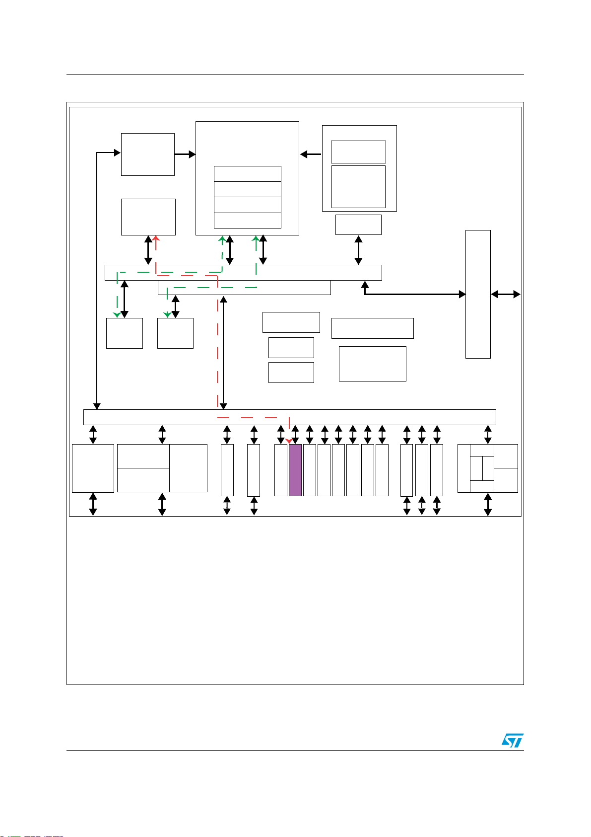
2.1 SPC564Ax CRC unit
The CRC unit allows the design of several self tests. When combined with the use of eDMA,
the self tests can be implemented without CPU load. This method is described in a specific
application note. The figure below illustrates the principle of this method and shows
concurrent accesses between CPU software using RAM and Flash together with the eDMA
and CRC unit.
Doc ID 16081 Rev 1 7/24
Page 8
Designing software self tests for SPC564Ax AN3018
Figure 1. CRC unit
)NTERRUPT
#O
CHANNEL
E$-!
3
-"
&LASH
3RZHU$UFKLWHFWXUH
EZ
NTROLLER
30%
6,%
--5
+")CACHE
- - -
-
#ROSSBAR3WITCH
-05
3 3
+"
!-
32
!NALOG0,,
2#/3#
8/3#
)/"RIDGE
$EBUG
*4!'
.EXUS
)%%%)34/
&LEX2AY
3
6OLTAGE2EGULATOR
#ALIBRATION"US)NTERFACE
3TANDBY
2EGULATOR
WITH3WITCH
E-)/3
#HANNEL
+"$ATA
-
2!
+"#ODE
2!-
E405
#HANNEL
2%!#-CH
0)4
$43
#2#
#2#
&-0,,
"!-
0-#
34-
374
3)5
)X
$30) X
E3#
&LEX#!. X
!$#I
!-UX
4E M P 3 E N S
!$#
$%#
X
!$#
6'!
/(*(1'
$'& ±$QDORJWR'LJLWDO&RQYHUWHU
$'&L ±$'&LQWHUIDFH
$0
X[ ±$QDORJ0XOWLSOH[HU
%$0 ±%RRW$VVLVW0RGXOH
&5& ±&\FOLF5HGXQGDQF\&KHFNXQLW
'(
& ±'HFLPDWLRQ)LOWHU
'76 ±'HYHORSPHQW7ULJJHU6HPDSKRUH
'63, ±'HVHULDO6HULDO3HULSKHUDO,QWHUIDFH
H'0$ ±(QKDQFHG'LUHFW0HPRU\$FFHVV
H0,
26 ±(QKDQFHG0RGXODU,QSXW2XWSXW6\VWHP
, ±(QKDQFHG6HULDO&RPPXQLFDWLRQV,QWHUIDFH
H6&
H738 ±6HFRQGJHQ(QKDQFHG7LPH3URFHVVLQJ8QLW
)OH[&$1±&RQWUROOHU$UHD1HWZRUN)OH[&$1
)03// ±)UHTXHQF\0RGXODWHG3KDVH/RFNHG/RRS
-7$* ±,(((7HVW&RQWUROOHU
008 ±0HPRU\0DQDJHPHQW8QLW
038 ±0HPRU\3URWHFWLRQ8QLW
30& ±3RZHU0DQDJHPHQW&RQWUROOHU
3,7 ±3HULRGLF,QWHUUXSW7LPHU
5&26
& ±/RZVSHHG5&2VFLOODWRU
5($&0 ±5HDFWLRQ0RGXOH
6,8 ±6\VWHP,QWHJUDWLRQ8QLW
63( ±6LJQDO3URFHVVLQJ([WHQVLRQ
65$0 ±6WDWLF5$0
670 ±6\VWHP7LPHU0RGXOH
6:7 ±6RIWZDUH:DWFKGRJ7LPHU
9*$ ±9DULDEOH*DLQ$PSOLILHU
9/( ±9DULDEOH/HQJWKLQVWUXFWLRQ(QFRGLQJ
;26& ±;7$/2VFLOODWRU
'!0'#&4
Note: The CRC unit has 3 independent contexts to allow independent CRC computing from CPU
side (for example, adding applicable CRC to data) and from eDMA.
8/24 Doc ID 16081 Rev 1
Page 9

AN3018 Designing software self tests for SPC564Ax
2.2 Explicit and implicit self tests
Most IPs can be checked with explicit tests. Some, like the crossbar and the peripheral
bridge, are tested implicitly through other self tests run on other modules.
Doc ID 16081 Rev 1 9/24
Page 10

Self tests for SPC564Ax core subsystem AN3018
3 Self tests for SPC564Ax core subsystem
3.1 Flash self tests
Several Flash tests can be implemented:
– Flash integrity test
– Flash ECC logic verification
– Flash address decoder
– Flash margin mode
Some SPC564Ax derivatives, like the 4 MB version, have two Flash modules. The tests
described below can be implemented on any of the flash modules in SPC564Ax devices.
Not having valid content in some of the memory locations of the sectors to be checked may
lead to limitation to flash sectors that do not have EEPROM data. This may happen for
sectors or data sets in EEPROM emulation area, as the programming or erasing may be
interrupted.
3.1.1 Flash integrity check
Principle: the Flash integrity test uses a proprietary address sequence to compute a 32-bit
signature over the flash content over selected flash sectors. The check includes user data
bits but also the ECC bits.
Result: once the operation is completed, the results of the reads can be checked by reading
the MISR value (stored in UMISR0-4), to determine if an incorrect read or ECC detection
was noted. The internal MISR calculator is a 32 bit register. The MISR can be seeded to any
value by initializing the UMISR0-4 registers before starting the test.
Resource availability: the Flash module is not available during this test.
The 128-bit data, 16-bit ECC data and the single and double ECC errors of the two double
words are therefore captured by the MISR through five different read accesses at the same
location. The whole check is done through five complete scans of the memory address
space:
1. The first pass scans only bits 31-0 of each page.
2. The second pass scans only bits 63-32 of each page.
3. The third pass scans only bits 95-64 of each page.
4. The fourth pass scans only bits 127-96 of each page.
5. The fifth pass scans only the ECC bits (8 + 8) and the single and double ECC errors (2
+ 2) of both double words of each page.
The 128-bit data and the 16 ECC data are sampled before the eventual ECC correction,
while the single and double error flags are sampled after the ECC evaluation.
Only data from existing and unlocked locations is captured by the MISR.
There is no restriction on the number of times the test can be performed.
For more details on this test, please refer to device reference manual (see Section A.1:
Reference documents).
10/24 Doc ID 16081 Rev 1
Page 11

AN3018 Self tests for SPC564Ax core subsystem
3.1.2 Flash ECC logic check1
Principle: ECC logic can be checked by forcing the input of ECC logic: The 64 bits of data
and the 8 bits of ECC syndrome can be forced individually through specific test registers.
The test then uses the ECC logic to produce a corrected 64-bit word.
Result: the results of the ECC logic check can be verified by reading the 64-bit results of the
corrected data in the flash UMISRx registers.
Resource availability: the Flash module is not available during this test.
As this is test based on standard flash memory reads, there is no restriction on the number
of times it can be performed.
For more details on this test, please refer to device reference manual (see Section A.1:
Reference documents).
3.1.3 Flash ECC logic check2
Principle: program a flash location to generate a single bit error and do reads during power
on or run time check. The procedure involves initially programming a memory location with
0xFFFF_FFFF_FFFF_FFFA and then programming the same memory location with
0xAAAA_AAAA_AAAA_AAAA. The resulting memory location will be
0xAAAA_AAAA_AAAA_AAAF with a dual bit error.
Result: a dual ECC error should be generated on bit0 and bit2.
Resource availability: the Flash module remains available during this test.
As this is test based on standard flash memory reads, there is no restriction on the number
of times it can be performed.
3.1.4 Flash ECC logic check3
Principle: program a flash location to generate a single bit error and do reads during power
on or run time check. The procedure involves initially programming a memory location with
0xFFFF_FFFF_FFFF_FFFE and then programming the same memory location with
0xAAAA_AAAA_AAAA_AAAA. The resulting memory location will be
0xAAAA_AAAA_AAAA_AAAB.
Result: a single ECC error should be generated on bit0.
Resource availability: the Flash module remains available during this test.
As this is test based on standard flash memory reads, there is no restriction on the number
of times it can be performed.
3.1.5 Flash address decoder
Principle: although the flash address decoder is indirectly checked during run time by the
proper execution of the application program, a specific test can be implemented by
inserting, at several places in the flash address space, data with known content. A signature
using the CRC unit of SPC564Ax can be computed by reading the flash content at those
places and writing them in the CRC unit. The CRC can be seeded to any value by initializing
the CRC before the test.
Result: once the test is completed, the signature in the CRC unit can be compared with the
reference signature.
Doc ID 16081 Rev 1 11/24
Page 12

Self tests for SPC564Ax core subsystem AN3018
Resource availability: the Flash module is available during this test.
There is no restriction on the number of times the test can be performed.
3.1.6 Flash margin mode
Principle: margin read is provided as a factory programming check; it can only be used at
25°C and only on a non-cycled flash. A direct read access may be performed at margin
(either margin 0 or margin 1), on unlocked blocks. The ‘Margin read’ operation makes it
possible to unbalance the sense amplifiers, so that all the read accesses reduce the margin
vs. ‘0’ (UT0.MRV = ‘0’) or vs. ‘1’ (UT0.MRV = ‘1’).
Result: the results of the margin reads can be checked by comparison with previously
stored expected data.
Resource availability: the Flash module is not available during this test.
The test can be performed only a limited number of times (up to 10 times maximum). It
should be reserved for OEM factory test and is not recommended for use in the field.
For more details on this test, please refer to device reference manual (see Section A.1:
Reference documents).
3.2 RAM self tests
Three RAM tests can be implemented:
– RAM dormant fault test
– RAM ECC logic verification
– RAM address decode
3.2.1 RAM dormant fault check
Principle: bit flip events in the RAM are detected and corrected by the ECC. When a RAM
memory location is not read, bit flip events may cumulate and generate an incorrigible error.
RAM dormant fault check can be implemented by reading regularly the whole content of the
RAM using the DMA controller.
Result: in case of error, an ECC event in the RAM is generated.
Resource availability: the RAM module is available during this test.
3.2.2 RAM ECC logic
RAM ECC covers the main system RAM.
Principle: The intent is to generate errors during data write cycles, so that subsequent
reads of the corrupted address locations generate ECC events, either single-bit corrections
or double-bit incorrigible errors that are terminated with an error response. RAM ECC test is
performed through the ECSM. The ECC error generation register is a 16-bit control register
used to force the generation of single and double bit data inversions in the memories with
12/24 Doc ID 16081 Rev 1
Page 13

AN3018 Self tests for SPC564Ax core subsystem
ECC, most notably the RAM. This capability is provided for two purposes:
– It provides a software controlled mechanism for “injecting” errors into the
memories during data writes to verify the integrity of the ECC logic
– It provides a mechanism to allow testing of the software service routines
associated with memory error logging
Result: after writing data with an erroneous ECC, the procedure involves reading back the
data and checking for error detection with the right parameters (single error, double error,
address of error).
Resource availability: once the RAM locations with erroneous content have been written,
the RAM is available for the application.
3.2.3 RAM address decoder
Principle: a specific test to check the RAM decoder can be implemented by inserting, at
several places in the RAM address space, data with known content. A signature using the
CRC unit of SPC564Ax can be computed by reading the RAM content at those places and
writing them in the CRC unit. The CRC can be seeded to any value by initializing the CRC
before the test.
Result: once the test is completed, the signature in the CRC unit can be compared with the
reference signature.
Resource availability: the RAM module is available during this test.
There is no restriction on the number of times the test can be performed.
3.2.4 eTPU code RAM
Principle: compute a signature over the eTPU code RAM during run time. Once enabled
(bits SCMMISEN=1 and bit VIS=0 in EPUTMCR register), this check is performed
continuously.
Result: the computed signature is automatically compared with a predefined signature in
EPTUMISCCMPR register. In case of mismatch, eTPU can also assert a global exception
interrupt indicating a global illegal state.
Resource availability: the eTPU code RAM is available during this test.
3.3 CPU parallel signature unit tests
The cores of SPC563Mx and of SPC564Ax devices have integrated signature registers to
enhance capabilities to develop core self tests.
To support applications requiring system integrity checking during operation, the Zen core
provides a parallel signature unit, which is capable of monitoring the CPU data read and
data write AHB buses, and accumulating a pair of 32-bit MISR signatures of the data values
transferred over these buses.
Doc ID 16081 Rev 1 13/24
Page 14

Self tests for SPC564Ax core subsystem AN3018
Figure 2. Parallel signature unit
.OTE
5PDATESDUETOQUALIFIEDBUSTRANSFERSARESUPPRESSED
FORTHEDURATIONOFADEBUGSESSION
$ATA"USP?D?HRDATAP?D?HWDATA
$$ $$$$$$$$$$$$$$$$
GT
GT
GT
GT
03(203,2
GT
GT
GT
GT
GT
'!0'#&4
Several CPU tests can be implemented:
– Register test
– Arithmetic and logic unit test
– Control flag test
– Branch test
The parallel, available on any SPC564Ax variant, allows the acceleration of the tests by
computing a signature and avoiding single register comparison to an external reference.
Principle: use software based tests to check the CPU core. Instead of comparing CPU
registers to a reference, use the CRC unit to compute a signature by writing the register
content to the CRC unit. The CRC can be seeded to any value by initializing the CRC before
the test.
Result: once the test is completed, the signature in the CRC unit can be compared with the
reference signature.
Resource availability: the CPU module is available during this test. Interrupts should be
masked during the execution of the test as the content of the parallel signature unit would be
modified during the execution of the interrupt routine.
14/24 Doc ID 16081 Rev 1
Page 15

AN3018 Self tests for SPC564Ax digital peripherals
4 Self tests for SPC564Ax digital peripherals
4.1 CRC unit self tests
The CRC unit is an essential module in the safety concept of SPC564Ax. It is made of two
submodules with independent register sharing the same computing circuitry.
CRC check should implement:
– Register check
– Computing circuitry check
4.1.1 CRC computing circuitry check
Principle: the computing circuitry can be checked by computing a CRC over the entire flash
content. The DMA controller can also be used to accelerate the test and execute it
concurrently with CPU initialization.
Result: once the test is completed, the signature in the CRC unit can be compared with the
reference signature.
Resource availability: the CRC module is not available during this test.
4.2 DMA controller self tests
The DMA controller is also an essential module in the safety concept of SPC564Ax. It is
made of 16 channel transfer descriptor registers sharing the same transfer logic.
DMA check should implement
– Register check
– Transfer logic check
4.2.1 DMA transfer logic check
Principle: the DMA transfer logic can be checked by means of complex transfer sequences.
If the application implements a peripheral configuration check using DMA and CRC, the
proposal is to have an implicit check using this test.
Result: once the test is completed, the signature in the CRC unit can be compared with the
reference signature.
Resource availability: the DMA module is available during this test. Only one channel can
be used by this test.
4.3 Crossbar self tests
SPC564Ax crossbar has a limited number of registers. Once configured properly, the
crossbar can be checked using implicit tests.
The crossbar can be implicitly tested when the following self tests have been implemented:
– Peripheral configuration check (see below)
– Flash and RAM check
Doc ID 16081 Rev 1 15/24
Page 16

Self tests for SPC564Ax digital peripherals AN3018
4.4 Memory protection self tests
SPC564Ax MPU is implemented using registers defining memory ranges and comparators.
In most safety applications, it is an important part of the safety concept as it isolates critical
data from non critical data.
The MPU can be explicitly tested using:
– Register test
– Functional tests
4.5 Peripheral bridge self test s
SPC564Ax peripheral bridge does not have a configuration register. It can be checked using
implicit tests.
The peripheral can be implicitly tested when the peripheral configuration self tests have
been implemented (see below).
4.6 Peripheral configuration self tests
Peripheral configuration check allows the implementation of two types of tests on
peripherals:
– Power on tests (latent fault monitor), by checking the value of each initialized
register
– Run time test, by checking the value of configuration registers with a fixed content
4.6.1 Peripheral configuration check
Principle: use the scatter/gather mode of the DMA controller, to chain several transfer
sequences, which read the peripheral registers to be checked and write them to the CRC
unit to compute a signature. The CRC can be seeded to any value by initializing the CRC
before the test.
Result: once the test is completed, the signature in the CRC unit can be compared with the
reference signature.
Resource availability when run as power on test: peripherals being checked are not
available during this test.
Resource availability when run as run time test: peripherals being checked are available
during this test.
This check makes intensive use of the peripheral bridge and DMA state machines (address
generator, chaining of DMA transfers).
4.7 Interrupt controller self tests
The interrupt controller plays an important role in an SPC564Ax application. Interrupt
controller check should implement:
– Register check
– Logic circuitry check
16/24 Doc ID 16081 Rev 1
Page 17

AN3018 Self tests for SPC564Ax digital peripherals
4.7.1 Interrupt controller logic check
Principle: the interrupt controller has a register to store the base address of the interrupt
vectors. The interrupt controller logic can be checked by defining a specific interrupt table for
the self tests. Software configurable interrupt sources can then be used to generate an
interrupt request. Nesting and priority management can be checked by enabling those
software configurable sources during selected interrupt routines.
Result: self test software dependent.
Resource availability: the interrupt controller is not available during this test.
Note: As interrupt controller is checked using software based tests, more complex self tests can
be generated if required.
4.8 FlexCAN self tests
FlexCAN module has a loop back mode. This mode can be used to implement a self test.
This test will exercise the protocol engine of the FlexCAN.
4.8.1 FlexCAN check
Principle: use the loop back mode of FlexCAN module to send and receive data without
sending it over the CAN network.
Result: transmitted message is received by FlexCAN and the content of the message
(message ID, message payload) can be compared to known value(s).
Resource availability: FlexCAN is not available during this test.
4.9 eSCI self tests
A loop back mode is available.
4.9.1 eSCI loop back
Principle: eSCI can be put in loop back mode by setting bit “LOOPS” and clearing bit
“RSRC” of register SCICR1. In loop back mode, the eSCI treats its own transmitted
messages as received messages.
Result: transmitted message is received by eSCI and the content of the message can be
compared to known value(s).
Resource availability: eSCI is not available during this test.
4.10 eMIOS self tests
eMIOS module generates real time input output events, such as, counting, capture,
compare. This module can be checked using the eTPU.
4.10.1 eMIOS check
Principle: use the eTPU to capture the characteristics of some eMIOS channels.
Doc ID 16081 Rev 1 17/24
Page 18

Self tests for SPC564Ax digital peripherals AN3018
Result: the captured value in eTPU must be compared to the known eMIOS characteristics
by taking account the prescaler factor used for eMIOS and eTPU.
Resource availability: this test requires allocation of eTPU channels for the check.
4.11 Decimation filter self tests
The decimation filter is able to perform computation on eQADC results. This module can be
checked using inputs from CPU or eDMA.
4.11.1 Decimation filter check
Principle: use CPU or eDMA to write inputs to the decimation filter.
Result: check results of the decimation filter at several stages of the “test filter”
computation.
Resource availability: the decimation filter is not available during this test.
4.12 eQADC logic self tests
eQADC logic can influence the conversion results if it generates an incorrect sampling time
and/or an incorrect conversion time.
Self tests should implement:
– Register test
– Effective eQADC conversion timing
4.12.1 eQADC effective conversion timing
Principle: configure the eQADC trigger unit to generate two consecutive ADC conversions
with time stamping for each conversion.
Result: the captured time stamps in eQADC results must be compared to the known
effective times of ADC conversion.
Resource availability: this test does not require specific resource provided a trigger is
available for this test.
18/24 Doc ID 16081 Rev 1
Page 19

AN3018 Self tests for SPC564Ax digital peripherals
4.13 Summary for digital peripherals
The table below summarizes the self tests for digital peripherals.
Table 1. Self tests for digital peripherals
Module Self test Comments
CPU core Use software based tests.
eTPU core Use software based tests. -
Flash integrity test.
Flash
RAM
Interrupt
controller
Peripheral
configuration
DMA
CRC
Flash ECC logic verification.
Flash address decoder.
Flash margin mode.
RAM dormant fault test.
RAM ECC logic verification.
RAM address decode.
Use an alternate vector table for interrupt
controller self tests.
Use DMA and CRC unit to compute a signature
on all initialized registers.
Use DMA and CRC unit to compute a signature
on registers with static configuration.
Explicit test on registers.
Implicit test if peripheral configuration self test is
implemented.
Explicit test on registers.
Implicit test if peripheral configuration self test is
implemented.
CRC unit can be used to
accelerate result verification.
-
-
-
-
-
-
Crossbar
MPU Explicit test on register and functional tests. -
Peripheral bridge
eMIOS Use eTPU to capture signal from eMIOS. -
ADC logic
FlexCAN Loop back. -
eSCI Loop back. -
Decimation filter
Implicit test if Flash, RAM and peripheral
configuration checks are implemented.
Implicit test if peripheral configuration self test is
implemented.
Use eQADC time stamping to capture effective
time of conversions.
Use CPU instead of eQADC as source for
operands.
Doc ID 16081 Rev 1 19/24
-
-
-
-
Page 20

Self tests for SPC564Ax analog peripherals AN3018
5 Self tests for SPC564Ax analog peripherals
5.1 Oscillator self tests
The oscillator of each SPC564Ax variant can be checked with the clock quality monitor.
5.1.1 Oscillator check
Principle: use the clock quality monitor to check the crystal clock.
Result: use status bit in clock monitor to detect a loss of clock (or use interrupt).
Resource availability: the crystal clock is available during this test.
5.2 FMPLL self tests
SPC564Ax devices have 1 FMPLL.
5.2.1 FMPLL check
Principle: use the clock quality monitor to check the FMPLL.
Result: use status bit in clock monitor to detect a loss of lock (or use interrupt).
Resource availability: the FMPLL is available during this test.
5.3 eQADC self tests
SPC564Ax devices have two ADCs with their own logic, which share the same analog
supply and reference.
5.3.1 eQADC internal reference check
Principle: SPC564Ax analog multiplexers have several internal signals available for self
tests: internal bandgap, VREF/2, VREF/4, 3/4 x VREF.
Result: obtained by checking the ADC conversion result.
Resource availability: the ADC is available during this test.
5.3.2 Analog input and ADC mux check
Principle: each eQADC has its own independent analog mux. Use the two ADCs to convert
the same analog input.
Result: obtained by checking the ADC conversion result from each ADC.
Resource availability: excluding the time needed for conversion, ADC are available during
this test.
5.3.3 Analog input and ADC mux check
Principle: fault (open, short) in the ADC analog input of the differential inputs and ADC mux
can be detected by using the pull up and pull down integrated in the eQADC.
20/24 Doc ID 16081 Rev 1
Page 21

AN3018 Self tests for SPC564Ax analog peripherals
Result: obtained by checking the ADC conversion result of the selected differential input.
Resource availability: selecting pull up and pull down may affect the precision of regular
conversions performed during the time they are activated.
5.4 Supply monitor self tests
SPC564Ax devices have supply monitors for 5 V, 3.3 V (internally generated) and 1.2 V.
The 1.2 V monitor is testable.
5.4.1 1.2 V monitor check
Principle: reset or interrupt can be selected for a 1.2 V loss. By enabling interrupt and
changing the trimmed value and its threshold, it is possible to test the 1.2 V monitor.
Result: a 1.2 V error is reported when the threshold of the monitor is set lower than 1.2 V.
Resource availability: 1.2 V monitor is not available during this test.
5.4.2 Monitor check using eQADC
Principle: the analog multiplexer allows for convertion of any of the supplies (5 V, 3.3 V,
1.2 V). This also includes the reference voltage for 1.2 V.
Result: obtained by checking the ADC conversion result.
Resource availability: all LVIs should be disabled during this test.
Note that the 1.2 V is derived from a reference independent of the ADC VREF, so that the
1.2 V check with ADC allows checking of the ADC reference voltage.
5.5 Summary for analog peripherals
The table below summarizes the self tests for analog peripherals.
Table 2. Self tests for analog peripherals
Module Self test Comments
PLL Use CQM -
ADC ADC reference check, ADC mux and analog input check -
1.2 V monitor Change the 1.2 V threshold. -
PMC
Oscillator Use CQM -
Use ADC to measure the supplies (5
peripherals
, 3.3 V, 1.2 V)
self tests for analog
-
Doc ID 16081 Rev 1 21/24
Page 22

Document management AN3018
Appendix A Document management
A.1 Reference documents
SPC564A70B4, SPC564A70L7 32-bit MCU family built on the embedded Power
Architecture
SPC564A80B4, SPC564A80L7 32-bit MCU family built on the embedded Power
Architecture
®
(Reference manual RM0068, Doc ID 18132)
®
(Reference manual RM0029, Doc ID 15177)
22/24 Doc ID 16081 Rev 1
Page 23

AN3018 Revision history
Revision history
Table 3. Document revision history
Date Revision Changes
15-May-2012 1 Initial release.
Doc ID 16081 Rev 1 23/24
Page 24

AN3018
U
D
W
D
W
S
O
U
T
R
G
A
Y,
D
E
G
Please Read Carefully:
Information in this document is provided solely in connection with ST products. STMicroelectronics NV and its subsidiaries (“ST”) reserve the
right to make changes, corrections, modifications or improvements, to this document, and the products and services described herein at any
time, without notice.
All ST products are sold pursuant to ST’s terms and conditions of sale.
Purchasers are solely responsible for the choice, selection and use of the ST products and services described herein, and ST assumes no
liability whatsoever relating to the choice, selection or use of the ST products and services described herein.
No license, express or implied, by estoppel or otherwise, to any intellectual property rights is granted under this document. If any part of this
document refers to any third party products or services it shall not be deemed a license grant by ST for the use of such third party products
or services, or any intellectual property contained therein or considered as a warranty covering the use in any manner whatsoever of such
third party products or services or any intellectual property contained therein.
NLESS OTHERWISE SET FORTH IN ST’S TERMS AND CONDITIONS OF SALE ST DISCLAIMS ANY EXPRESS OR IMPLIE
ARRANTY WITH RESPECT TO THE USE AND/OR SALE OF ST PRODUCTS INCLUDING WITHOUT LIMITATION IMPLIE
ARRANTIES OF MERCHANTABILITY, FITNESS FOR A PARTICULAR PURPOSE (AND THEIR EQUIVALENTS UNDER THE LAW
F ANY JURISDICTION), OR INFRINGEMENT OF ANY PATENT, COPYRIGHT OR OTHER INTELLECTUAL PROPERTY RIGHT.
NLESS EXPRESSLY APPROVED IN WRITING BY TWO AUTHORIZED ST REPRESENTATIVES, ST PRODUCTS ARE NO
ECOMMENDED, AUTHORIZED OR WARRANTED FOR USE IN MILITARY, AIR CRAFT, SPACE, LIFE SAVING, OR LIFE SUSTAININ
PPLICATIONS, NOR IN PRODUCTS OR SYSTEMS WHERE FAI LURE OR MALFUNCTION MAY RESULT IN PERSONAL INJUR
EATH, OR SEVERE PROPERTY OR ENVIRONMENTAL DAMAGE. ST PRODUCTS WHICH ARE NOT SPECIFIED AS "AUTOMOTIV
RADE" MAY ONLY BE USED IN AUTOMOTIVE APPLICATIONS AT USER’S OWN RISK.
Resale of ST products with provisions different from the statements and/or technical features set forth in this document shall immediately void
any warranty granted by ST for the ST product or service described herein and shall not create or extend in any manner whatsoever, any
liability of ST.
The ST logo is a registered trademark of STMicroelectronics. All other names are the property of their respective owners.
ST and the ST logo are trademarks or registered trademarks of ST in various countries.
Information in this document supersedes and replaces all information previously supplied.
© 2012 STMicroelectronics - All rights reserved
STMicroelectronics group of companies
Australia - Belgium - Brazil - Canada - China - Czech Republic - Finland - France - Germany - Hong Kong - India - Israel - Italy - Japan -
Malaysia - Malta - Morocco - Philippines - Singapore - Spain - Sweden - Switzerland - United Kingdom - United States of America
www.st.com
24/24 Doc ID 16081 Rev 1
 Loading...