

Page 1
AN3008
Application note
STOD2540, single inductor DC-DC converter
generates multiple supply voltages for E-paper display
Introduction
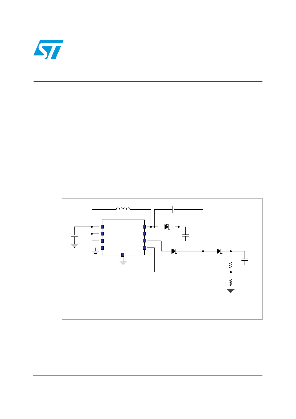
This application note describes how to use the STOD2540 DC-DC converter to generate
two output voltages using a single inductor and an external charge pump. The circuit shown
in Figure 1 generates a 70 V output from a 3.7 V input voltage.
The STOD2540 is a highly integrated boost converter that can provide an adjustable output
up to 35 V from a 3.0 to 5.5 V input voltage.
The STOD2540 operates in PFM (pulsed frequency modulation) mode. PFM control simply
means that the part only switches when the charge needs to be delivered to the output in
order to keep the output voltage regulated.
The converter is ideal for generating the necessary voltages to supply thin-film transistor
(TFT) LCDs, OLEDs and E-paper shelf labels. The low operating supply current makes the
device ideal for small, portable, battery supplied applications. In shutdown mode the load is
disconnected from the input and the quiescent current is less than 3 µA.
Figure 1. High voltage power supply based on STOD2540
C1
C1
D1
D1
C2
C2
1
1
7
CIN
CIN
CIN: 4.7μF
CIN: 4.7μF
COUT: 2 x 1 μF 100 V
COUT: 2 x 1 μF 100 V
C1: 100 nF 50 V
C1: 100 nF 50 V
C2: 4.7 μF 50 V
C2: 4.7 μF 50 V
L1: 4.7 μH
L1: 4.7 μH
D1, D2, D3: STPS2L40AF
D1, D2, D3: STPS2L40AF
7
2
2
3
3
STOD2540
STOD2540
U1
U1
VIN
VIN
ENABLE
ENABLE
RSET
RSET
AGND
AGND
L1
L1
8
8
SW
SW
6
6
Vcap
Vcap
5
5
Vo
Vo
4
4
FB
FB
PGND
PGND
9
9
D3D2
D3D2
COUT
R3
R3
550k
550k
R4
R4
10k
10k
COUT
January 2010 Doc ID 16021 Rev 2 1/14
www.st.com
Page 2

Contents AN3008
Contents
1 High voltage power supply based on STOD2540 . . . . . . . . . . . . . . . . . . 3
1.1 STOD2540 function description . . . . . . . . . . . . . . . . . . . . . . . . . . . . . . . . . 3
1.2 Load disconnect . . . . . . . . . . . . . . . . . . . . . . . . . . . . . . . . . . . . . . . . . . . . . 3
1.3 Output adjust . . . . . . . . . . . . . . . . . . . . . . . . . . . . . . . . . . . . . . . . . . . . . . . 3
1.4 Inductor selection . . . . . . . . . . . . . . . . . . . . . . . . . . . . . . . . . . . . . . . . . . . . 4
1.5 C
1.6 Diode selection . . . . . . . . . . . . . . . . . . . . . . . . . . . . . . . . . . . . . . . . . . . . . . 5
1.7 Single inductor circuit based on STOD2540 derives 35 V / 70 V . . . . . . . . 5
selection . . . . . . . . . . . . . . . . . . . . . . . . . . . . . . . . . . . . . . . . . . . . . . 4
OUT
2 Test results . . . . . . . . . . . . . . . . . . . . . . . . . . . . . . . . . . . . . . . . . . . . . . . . 7
2.1 Start-up . . . . . . . . . . . . . . . . . . . . . . . . . . . . . . . . . . . . . . . . . . . . . . . . . . . 7
2.2 Output voltage ripple . . . . . . . . . . . . . . . . . . . . . . . . . . . . . . . . . . . . . . . . . 7
2.3 Efficiency . . . . . . . . . . . . . . . . . . . . . . . . . . . . . . . . . . . . . . . . . . . . . . . . . . 8
2.4 Line regulation 70 V / 35 V . . . . . . . . . . . . . . . . . . . . . . . . . . . . . . . . . . . . . 8
2.5 Load regulation . . . . . . . . . . . . . . . . . . . . . . . . . . . . . . . . . . . . . . . . . . . . . 9
3 Layout . . . . . . . . . . . . . . . . . . . . . . . . . . . . . . . . . . . . . . . . . . . . . . . . . . . . 10
3.1 Input / output connections . . . . . . . . . . . . . . . . . . . . . . . . . . . . . . . . . . . . 11
4 Application schematic and bill of materials . . . . . . . . . . . . . . . . . . . . . 12
5 Revision history . . . . . . . . . . . . . . . . . . . . . . . . . . . . . . . . . . . . . . . . . . . 13
2/14 Doc ID 16021 Rev 2
Page 3

AN3008 High voltage power supply based on STOD2540
1 High voltage power supply based on STOD2540
1.1 STOD2540 function description
The STOD2540 uses a PFM control scheme to reach high efficiency in low load conditions.
The DC-DC has a current mode control scheme that uses a minimum OFF time and a
maximum ON time.
The converter monitors the output voltage through the resistor dividers R1 and R2 by
comparing the feedback voltage with the internal reference voltage of 1.24 V.
The integrated main power switch is turned on as soon as the feedback voltage falls below
the internal reference. The switch stays on until the inductor current reaches the peak
current limit or for a maximum ON time equal to 5.5 µsec. The peak current limit value is
adjustable through an external resistor connected between the RSET pin and GND. The
main switch stays off for at least a minimum OFF time (300 ns typical) and remains in the off
state for as long as the feedback voltage remains above the internal reference voltage.
During the ON time, the load current is only supplied by the charge stored in the output
capacitor until the feedback voltage drops below the reference voltage again.
PFM regulation is particularly useful when output currents are low and the part is prevalently
in the OFF state.
1.2 Load disconnect
When the device is in shutdown mode, a DC current path exists between the power source
and the load. A high-side switch LDS isolates the load from the source when the device is
disabled.
1.3 Output adjust
Choose the R4 value in the range of 10 to 200 kΩ. The value of R3 can be calculated from
the following equation.
Equation 1
FB
−×= 1
⎞
⎟
⎟
⎠
⎛
V
OUT
⎜
RR
LU
⎜
V
⎝
Where
R
is the upper resistor of the voltage divider.
U
R
is the lower resistor of the voltage divider.
L
1% tolerance resistors should be chosen for a more accurate V
The STOD2540 shows a pulses burst behavior that causes a high output voltage ripple. To
decrease the output ripple it is possible to insert a capacitor across the upper feedback
resistor. The following formula can be used to obtain a first estimation of the value of the
capacitor.
OUT
.
Doc ID 16021 Rev 2 3/14
Page 4

High voltage power supply based on STOD2540 AN3008
Equation 2
CF
=
2
1
F
SW
R
××π×
20
U
Where
R
is the upper resistor of the voltage divider.
U
F
is the switching frequency.
SW
The following equation gives the switching frequency at the nominal load current.
Equation 3
)VV(I2
−××
)I(F
=
LOADSW
2
IL
×
PK
INOUTLOAD
The CF capacitor increases the amplitude of the voltage ripple on the FB pin, causing a
deterioration of the line regulation; therefore, the value of CF should be as small as possible.
1.4 Inductor selection
Since the hysteretic control scheme is inherently stable, the inductor value does not affect
the stability of the regulator. Using the PFM peak current control scheme, the converter
operates in discontinuous conduction mode (DCM).
The inductance value must be calculated so as to ensure that the inductor current reaches
the current limit before the maximum ON time expires. The following equation can be used
to calculate the maximum value of the inductance.
Equation 4
L ×≤
Where IPK is the controlled inductor peak current.
In this case the maximum value of the load current is given by
Equation 5
I
1.5 C
The output voltage ripple very much depends on the application conditions. The output
capacitor has a significant effect on the output voltage ripple magnitude because it supplies
the load current through the charge stored during the ON state.
V
I
PK
MAX_LOAD
selection
OUT
MIN_IN
T
MAX_ON
Equation 5.
2
×
LI
=
PK
⎛
×
LI
PK
⎜
×−+×
)VVdV(2
INOUT
⎜
⎝
+
V
IN
toff
MIN
⎞
⎟
⎟
⎠
The output voltage ripple consists of two parts: the first is caused by the ESR, the second by
the charging and discharging process of the output capacitor.
4/14 Doc ID 16021 Rev 2
Page 5
AN3008 High voltage power supply based on STOD2540
The output ripple can be approximately given by the following equation.
Equation 6
V
OUT
I
C
OUT
⎛
1
⎜
−×=Δ
⎜
F
SWOUT
⎝
PK
×
⎞
LI
⎟
⎟
−+
VVV
INDOUT
⎠
The magnitude of the ripple will typically be linearly proportional to the output capacitance
present. For the best output voltage filtering, a low ESR output capacitor is recommended.
1.6 Diode selection
The output diode in a boost converter conducts current only when the power switch is off.
The average current is equal to the output current and the maximum current is equal to the
peak inductor current.
To maximize efficiency, we recommend using a Schottky diode characterized by:
1. a small forward voltage drop.
2. a rated current larger than the peak inductor current.
3. a reverse voltage larger than the output voltage.
4. a small reverse leakage current.
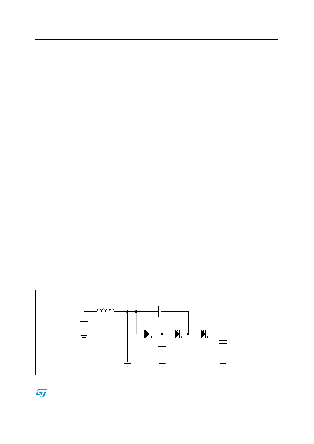
1.7 Single inductor circuit based on STOD2540 derives 35 V/70 V
The circuit shown in Figure 2 is capable of deriving +35 / +70 V from a [3; 5.5] input voltage
range. The STOD2540 DC-DC converter generates the 35 V output voltage. The addition of
an external charge pump consisting of two Schottky diodes (D2 and D3) and two capacitors
(C1 and C2) allows delivering output voltages of over 70 V.
In steady-state operation, the voltage on C2 is 35 V and the voltage on C
the ON time the main switch is closed and the current flows from the input to ground through
L1 and the internal switch. During this time, the voltage at node SW is 0 V and C1 is charged
up to 35 V. In these conditions, D1 is reverse-biased, D2 is forward-biased, D3 is reversebiased and the load current is supplied only by the output capacitor C
Figure 2. External charge pump - TON state
L1
CIN
CIN
L1
SW = 0 V
SW = 0 V
Doc ID 16021 Rev 2 5/14
D1
D1
C1
C1
35 V
35 V
is 70 V. During
OUT
.
OUT
+
+
+
+
35 V
35 V
70 V
70 V
COUT
COUT
C2
C2
D3D2
D3D2
Page 6

High voltage power supply based on STOD2540 AN3008
Figure 3. External charge pump - T
L1
L1
SW = 35 V
SW = 35 V
CIN
CIN
When the power switch is opened, D1 is forward-biased and current flows through L1 and
D1 into C2. Therefore, the voltage at node SW is equal to the voltage on C2 (35 V).
C1, which was previously charged to 35 V, is now referenced to node 35 V. The voltage
across C1 remains at 35 V, but the left side is 35 V with respect to ground and the right side
is 70 V with respect to ground. D3 becomes forward-biased and C
is reverse-biased during this time period.
The output is regulated to 70 V through the feedback divider that goes back to the FB pin of
the STOD2540. An unregulated output voltage of 35 V is available from the C2 output
capacitor in this configuration. Since the 35 V output voltage is not regulated, it is not stable
like the 70 V output voltage and varies with the current drawn from the 70 V.
OFF
state
D1
D1
C1
C1
35 V
35 V
35 V
35 V
+
+
+
+
70 V
C2
C2
70 V
D3D2
D3D2
70 V
70 V
COUT
COUT
is charged to 70 V. D2
OUT
If desired, the feedback can be recalculated for a 35 V output. This provides a regulated
35 V output and an unregulated 70 V output.
D1, D2 and D3 must be rated for at least half the higher output voltage. The peak current
ratings for the diodes must be greater than half the peak switch current of the STOD2540.
C2 and C3 must have voltage ratings greater than half the output voltage, while C4 must be
rated for the full output voltage.
6/14 Doc ID 16021 Rev 2
Page 7

AN3008 Test results
2 Test results
2.1 Start-up
Figure 4 and Figure 5 show the output voltage and inductor current waveforms of the
evaluation module in the following conditions.
● V
● V
● I
Figure 4. Start-up/V
= 3.7 V
IN
OUT
LOAD
= 73 V
= 5 mA
OUT
Figure 5. Start-up/inductor current
2.2 Output voltage ripple
The traces in Figure 6 and Figure 7 show the output voltage ripple on a 70 V output with
different input voltages and I
Figure 6. 70 V output voltage ripple vs. V
V
= 5 V
V
= 5 V
IN
IN
V
V
= 4.2 V
= 4.2 V
IN
IN
V
V
= 3.7 V
= 3.7 V
IN
IN
V
V
= 3.2 V
= 3.2 V
IN
IN
equal to 10 mA.
LOAD
IN
Figure 7. 70 V output voltage ripple vs. I
NO LOAD
NO LOAD
5 mA
5 mA
10 mA
10 mA
LOAD
Doc ID 16021 Rev 2 7/14
Page 8

Test results AN3008
2.3 Efficiency
Figure 8. Output efficiency for the 70 V output
85%
Efficiency - %
Efficiency - %
85%
80%
80%
3V
3V
V
V
IN
75%
75%
70%
70%
65%
65%
60%
60%
55%
55%
02468101214161820
02468101214161820
IN
3,2 V
3,2 V
V
V
IN
IN
V
V
IN
IN
VIN3,7V
VIN3,7V
4,2 V
4,2 V
I
I
LOAD
LOAD
mA
mA
2.4 Line regulation 70 V / 35 V
Figure 9. 70 V line regulation Figure 10. 35 V line regulation
73.0
73.0
72.8
72.8
72.6
72.6
72.4
72.4
VOUT - V
VOUT - V
72.2
72.2
72.0
72.0
Load 1 mA
Load 1 mA
VOUT 70 V
VOUT 70 V
3.0 3.5 4.0 4.5 5.0 5.5
3.0 3.5 4.0 4.5 5.0 5.5
VIN - V
VIN - V
37.0
37.0
36.8
36.8
36.6
36.6
36.4
36.4
VOUT - V
VOUT - V
36.2
36.2
VOUT 35 V
VOUT 35 V
36.0
36.0
3.0 3.5 4.0 4.5 5.0 5.5
3.0 3.5 4.0 4.5 5.0 5.5
Load 1 mA on 70 V output
Load 1 mA on 70 V output
VIN - V
VIN - V
8/14 Doc ID 16021 Rev 2
Page 9

AN3008 Test results
2.5 Load regulation
Figure 11. 70 V output load regulation Figure 12. 35 V output changes when load
73.2
73.2
73.0
73.0
72.8
72.8
-V
-V
72.6
72.6
OUT
OUT
V
V
72.4
72.4
72.2
72.2
VIN= 3.7 V
VIN= 3.7 V
72.0
72.0
024681012141618
024681012141618
I
I
LOAD
LOAD
mA
mA
37.0
37.0
36.8
36.8
-V
-V
36.6
36.6
OUT
OUT
V
V
36.4
36.4
36.2
36.2
36.0
36.0
current is drowned from the 70 V
VIN= 3.7 V
VIN= 3.7 V
024681012141618
024681012141618
Figure 13 shows the behavior of the 35 V output when the load current is drowned from 35 V
and the FB pin is closed on 70 V.
Figure 13. 35 V unregulated output
I
I
LOAD
LOAD
mA
mA
40
40
40
35
35
35
30
30
30
VOUT - V
VOUT - V
VOUT - V
25
25
25
VIN= 3.7 V
VIN= 3.7 V
20
20
20
0 2 4 6 8 1012141618202224
0 2 4 6 8 1012 141618202224
0 2 4 6 8 1012 141618202224
I
I
I
LOAD
LOAD
LOAD
mA
mA
mA
Doc ID 16021 Rev 2 9/14
Page 10

Layout AN3008
3 Layout
To minimize the occurrence of problems related to noise and duty cycle jitter, attention has
been given to the routing of high-frequency current loops. It is essential to keep the high
switching current circulating paths as small as possible. In general the following rules should
be applied.
● The GND connections of the COUT, CIN capacitors and STOD2540 PGND should be
placed as close as possible to each other.
● The connection from the IC pins (VIN, SW) and the inductor must be kept short.
● CIN should be placed close to the VIN pin of the chip.
● The ground area should be as large as possible. If a two-layer PCB is used, one layer
should be assigned as the ground layer and a good connectivity between both layers
should be observed.
Figure 14. Assembly layer
Figure 15. Top layer
10/14 Doc ID 16021 Rev 2
Page 11

AN3008 Layout
Figure 16. Bottom layer
3.1 Input / output connections
Table 1. Input / output connections
Reference
designator
JP1 VIN/GND
Name Description
VIN: positive connection to the input power supply.
return connection to the input power supply.
GND:
Use this connector to enable and disable the DC-DC converter. Connect the EN
JP2 En
pin to GND to disable the converter. If the EN pin is left floating, the EVM
operates correctly.
HV: high voltage – 70 V. Positive connection for the load.
JP3 V
OUT
MV: medium voltage – 35 V. Positive connection for the load.
return pin for the load.
GND:
Doc ID 16021 Rev 2 11/14
Page 12

Application schematic and bill of materials AN3008
4 Application schematic and bill of materials
Figure 17. Demonstration board schematic
VIN
VIN
GND
GND
GND
GND
L1
L1
U1
J1
J1
1
1
2
2
CIN
CIN
R1
R1
0
0
J2
J2
EN
EN
1
1
2
2
U1
1
1
V
V
IN
IN
7
7
ENABLE
ENABLE
2
2
RSET
RSET
3
3
R2
R2
AGND
AGND
STOD2540
STOD2540
PGND
PGND
9
9
SW
SW
8
8
SW
SW
6
6
V
V
CAP
CAP
5
5
V
V
O
O
4
4
FB
FB
MV
MV
C1
C1
J3 OUT
D1
D1
C2
C2
D2
D2
D3
D3
CF
R3
R3
R5
R5
R4
R4
CF
GND
GND
MV
MV
HV
HV
COUT1
COUT1
J3 OUT
1
1
2
2
3
3
HV
HV
COUT2
COUT2
Table 2. Bill of materials
Quantity Reference Description Part/Value PCB Footprint
1 U1 DC-DC converter STOD2540PMR QFN8 3 x 3 mm
1 CIN Capacitor, ceramic, 4.7 µF, 16 V, X5R 0805
1 C1 Capacitor, ceramic, 100 nF, 50 V, X5R 0805
2 COUT Capacitor, ceramic, 1 µF, 100 V, X5R GRM31CR72A105KA01L 0805
1 CF Capacitor, ceramic, 47 pF 0603
1 L1 Inductor, 4.7 µH LPS3314-472MLC
3 D1, D2, D3 Diode, Schottky 2 A 30 V STPS2L40AF SMAflat
1 R1 Resistor, 1 kΩ, 1/16 W, 1% 0603
1 R2 Resistor, 1/16 W, 1% 0603
1 R3 Resistor, 680 kΩ, 1/16 W, 1% 0603
1 R4 Resistor, 10 kΩ, 1/16 W, 1% 0603
1 R5 Potentiometer, 100 kΩ
2 JP1, JP2 Header, 2-pin, 100-mil spacing
1 JP3 Header, 3-pin, 100-mil spacing
12/14 Doc ID 16021 Rev 2
Page 13

AN3008 Revision history
5 Revision history
Table 3. Document revision history
Date Revision Changes
10-Nov-2009 1 Initial release.
08-Jan-2010 2
Modified: Figure 14 on page 10, Figure 15 on page 10, Figure 16 on
page 11, Figure 17 and Table 2 on page 12.
Doc ID 16021 Rev 2 13/14
Page 14

AN3008
Please Read Carefully:
Information in this document is provided solely in connection with ST products. STMicroelectronics NV and its subsidiaries (“ST”) reserve the
right to make changes, corrections, modifications or improvements, to this document, and the products and services described herein at any
time, without notice.
All ST products are sold pursuant to ST’s terms and conditions of sale.
Purchasers are solely responsible for the choice, selection and use of the ST products and services described herein, and ST assumes no
liability whatsoever relating to the choice, selection or use of the ST products and services described herein.
No license, express or implied, by estoppel or otherwise, to any intellectual property rights is granted under this document. If any part of this
document refers to any third party products or services it shall not be deemed a license grant by ST for the use of such third party products
or services, or any intellectual property contained therein or considered as a warranty covering the use in any manner whatsoever of such
third party products or services or any intellectual property contained therein.
UNLESS OTHERWISE SET FORTH IN ST’S TERMS AND CONDITIONS OF SALE ST DISCLAIMS ANY EXPRESS OR IMPLIED
WARRANTY WITH RESPECT TO THE USE AND/OR SALE OF ST PRODUCTS INCLUDING WITHOUT LIMITATION IMPLIED
WARRANTIES OF MERCHANTABILITY, FITNESS FOR A PARTICULAR PURPOSE (AND THEIR EQUIVALENTS UNDER THE LAWS
OF ANY JURISDICTION), OR INFRINGEMENT OF ANY PATENT, COPYRIGHT OR OTHER INTELLECTUAL PROPERTY RIGHT.
UNLESS EXPRESSLY APPROVED IN WRITING BY AN AUTHORIZED ST REPRESENTATIVE, ST PRODUCTS ARE NOT
RECOMMENDED, AUTHORIZED OR WARRANTED FOR USE IN MILITARY, AIR CRAFT, SPACE, LIFE SAVING, OR LIFE SUSTAINING
APPLICATIONS, NOR IN PRODUCTS OR SYSTEMS WHERE FAILURE OR MALFUNCTION MAY RESULT IN PERSONAL INJURY,
DEATH, OR SEVERE PROPERTY OR ENVIRONMENTAL DAMAGE. ST PRODUCTS WHICH ARE NOT SPECIFIED AS "AUTOMOTIVE
GRADE" MAY ONLY BE USED IN AUTOMOTIVE APPLICATIONS AT USER’S OWN RISK.
Resale of ST products with provisions different from the statements and/or technical features set forth in this document shall immediately void
any warranty granted by ST for the ST product or service described herein and shall not create or extend in any manner whatsoever, any
liability of ST.
ST and the ST logo are trademarks or registered trademarks of ST in various countries.
Information in this document supersedes and replaces all information previously supplied.
The ST logo is a registered trademark of STMicroelectronics. All other names are the property of their respective owners.
© 2010 STMicroelectronics - All rights reserved
STMicroelectronics group of companies
Australia - Belgium - Brazil - Canada - China - Czech Republic - Finland - France - Germany - Hong Kong - India - Israel - Italy - Japan -
Malaysia - Malta - Morocco - Philippines - Singapore - Spain - Sweden - Switzerland - United Kingdom - United States of America
www.st.com
14/14 Doc ID 16021 Rev 2
 Loading...