

Page 1

AN2995
Demonstration board user guidelines
for single operational amplifiers
Introduction
This demonstration board is designed to help in the characterization of single operational
amplifiers in SOT23-5 (two different pinouts) and SC70-5 packages. Operational amplifiers
in SOT23-6 and SC70-6 packages can also be characterized, but their respective standby
pin cannot be used since it is connected to V
This document provides:
■ a brief description of the demonstration board.
■ a layout of the top and bottom layers.
■ some examples of typical configurations that can be tested with the board.
+ on the board.
CC
June 2009 Doc ID 15840 Rev 1 1/13
www.st.com
Page 2
Board description AN2995
1 Board description
This board is designed with versatility in mind. In particular, its components allow it to be
configured as:
● a low-pass Sallen-Key circuit.
● a high-pass Sallen-Key circuit.
● a differential amplifier.
● an AC-coupled circuit.
● an in-loop compensation circuit.
● an out-of-loop compensation circuit.
● and numerous other possible configurations not described here.
The board is designed for surface-mounted components in SOT23-5 (and SOT23-6) or
SC70-5 (SC70-6) packages. It can be used to perform on-board characterization prior to the
integration of STMicroelectronics’ products in your designs. Resistor and capacitor
footprints are implemented in the 0805 series.
A set of two decoupling capacitors have been implemented on both power supply pins so as
to benefit from the maximum performances of ST products. In order to reject a wide range of
frequencies, 100 nF and 4.7 µF are good values for these capacitors.
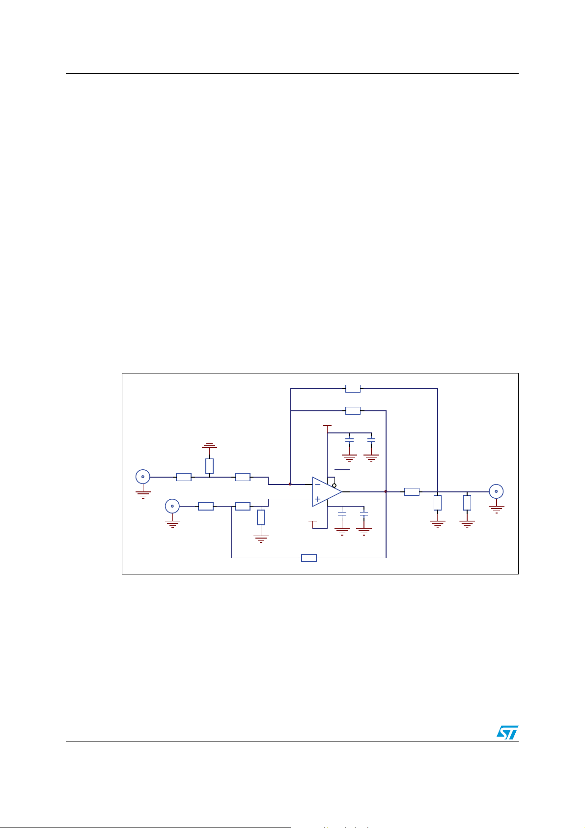
Figure 1. Demonstration board schematics
Z14
Z4
VCC+
C1
C2
Vin2
Z8 Z3
Vin1
Z1
Z9
Z2
Z5
Vcc+
VCC-
Z6
SHDN
OP AMP
C3 C4
Z13
Vout
Z7 Z12
AM04501
2/13 Doc ID 15840 Rev 1
Page 3
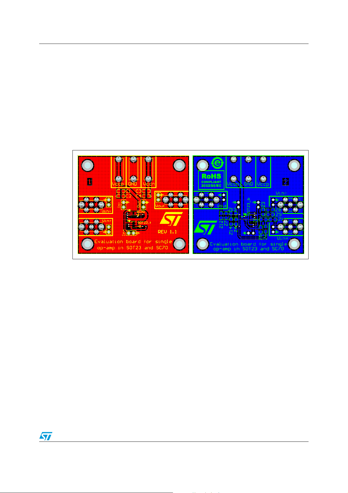
AN2995 Board layout
2 Board layout
The board has the following physical characteristics.
● Board dimensions: 2080 x 1900 mils (52.8 x 48.3 mm).
● 2-layer PCB.
For Vout, Vin1 and Vin2, male SMB or 2-mm female connectors can be implemented. You
can also implement test points on these three voltages to facilitate visualization of your
signals.
Figure 2 shows the top and bottom layers of the board.
Figure 2. Top and bottom layers
Doc ID 15840 Rev 1 3/13
Page 4
Possible configurations AN2995
3 Possible configurations
This chapter provides instructions on how to set-up the board with several typical
configurations.
● Figure 3: low-pass Sallen-Key configuration
● Figure 4: high-pass Sallen-Key configuration
● Figure 5: differential amplifier configuration
● Figure 6: in-loop compensation configuration
● Figure 7: out-of-loop compensation configuration
● Figure 8: AC-coupled configuration
You can also connect several boards together if you need to evaluate more complicated
schematics using several operational amplifiers.
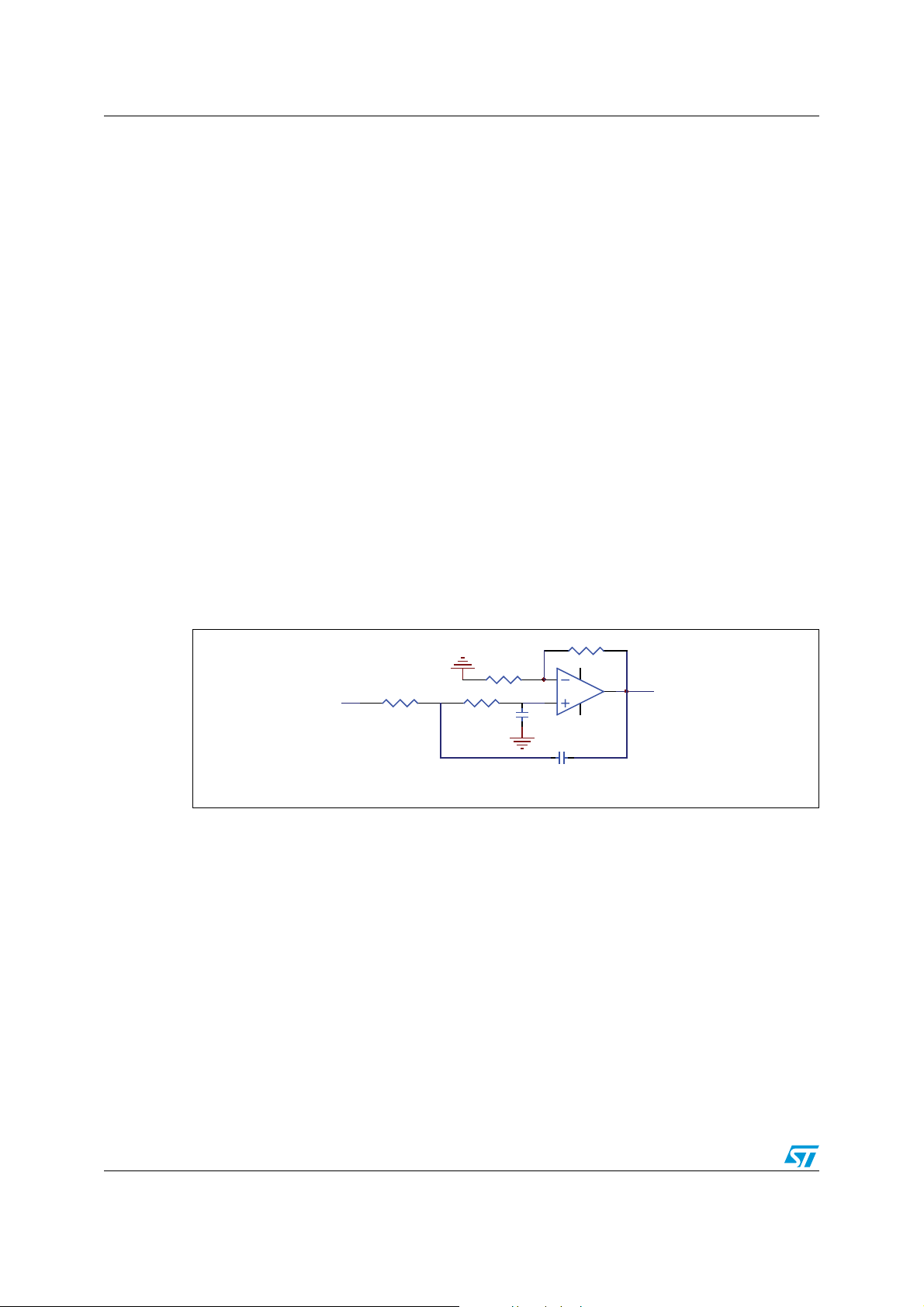
3.1 Low-pass Sallen-Key configuration
The low-pass Sallen-Key configuration is a second-order filter configuration. Z4 and Z9 are
used to set the gain.
Fc = 1/(2*PI*sqrt(Z1*Z2*C5*C6))
Z7, Z8, Z12 and Z14 must be "not connected". Z3 and Z13 must be shorted.
Figure 3. Low-pass Sallen-Key configuration
Z9
Vin1
Z2Z1
Z5
3.2 High-pass Sallen-Key configuration
Like the low-pass Sallen Key configuration, this is also a second-order filter configuration.
Z4 and Z9 are used to set the gain.
Fc = 1/(2*PI*sqrt(C1*C2*Z5*Z6))
Z7, Z8, Z12 and Z14 must be "not connected". Z3 and Z13 must be shorted.
Z4
Vout
Z6
AM04502
4/13 Doc ID 15840 Rev 1
Page 5
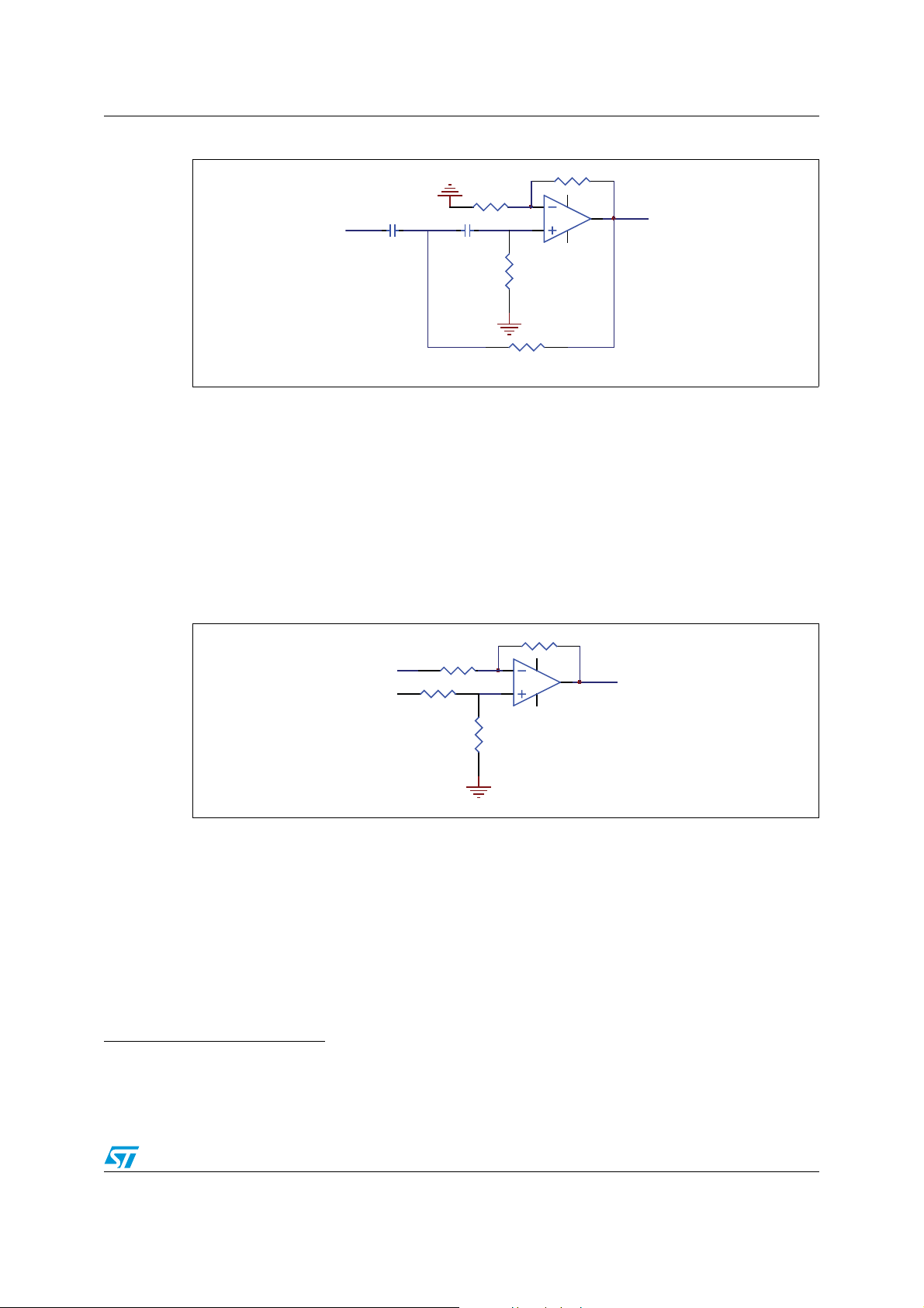
AN2995 Possible configurations
Figure 4. High-pass Sallen-Key configuration
Z4
Z9
Vin1
Z1 Z2
Vout
Z5
Z6
AM04503
3.3 Differential amplifier configuration
The differential amplifier configuration allows the subtraction of two voltages.
The transfer function is: Vout = Vin1 ((Z8+Z4)/Z8 * Z5/(Z1+Z5)) - Z4/Z8*Vin2.
Choosing Z8 = Z1 and Z4 = Z5 gives:
Vout = (Vin1-Vin2)*Z4/Z8
Z6, Z7, Z9, Z12 and Z14 must be "not connected". Z2, Z3 and Z13 must be shorted.
Figure 5. Differential amplifier configuration
Z4
Vin2
Vin1
Z8
Z1
Z5
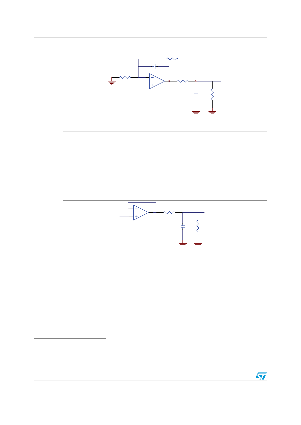
3.4 In-loop compensation configuration
The goal of this compensation technique is to stabilize an amplifier configuration with a
capacitive load. This compensation is called in-loop because the additional components
(Z13 and Z4) used to improve the stability are inserted in the feedback loop.
Z5, Z6 and Z8 must be "not connected". Z1, Z2 and Z3 must be shorted.
Vout
AM04504
(a)
a. More information on compensation methods can be found in application note AN2653: Operational amplifier stability
compensation methods for capacitive loading applied to TS507 (see Table 2: Document references).
Doc ID 15840 Rev 1 5/13
Page 6
Possible configurations AN2995
Figure 6. Compensation: in-loop configuration
Z14
Z4
Z9
Z13
Vin1
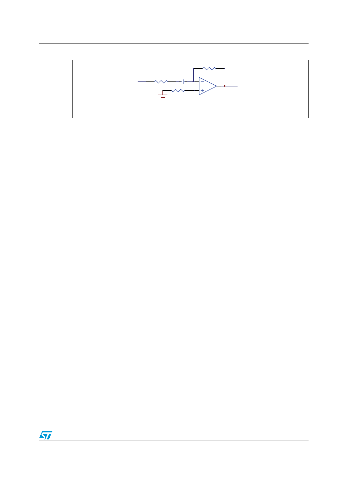
3.5 Out-of-loop compensation configuration
A simple compensation method, using only one extra component, consists in adding a
resistor (Z13) in series between the output of the amplifier and its load. It is often referred to
as the out-of-loop compensation method because the additional component is added
outside of the feedback loop.
Z3, Z5, Z6, Z8, Z9 and Z14 must be "not connected". Z1, Z2 and Z4 must be shorted.
Figure 7. Compensation: out-of-loop configuration
Z13
Vin1
Z7
(b)
Vout
Z12
AM04505
Vout
Z12
Z7
AM04506
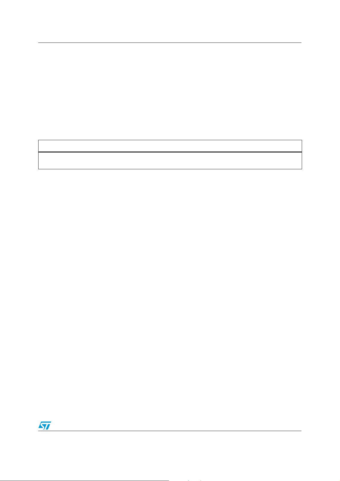
3.6 AC-coupled circuit configuration
This typical configuration allows you to amplify the AC part only of the input signal. Z2, Z6,
Z7, Z9, Z12 and Z14 must be "not connected". No component is shorted.
b. More information on compensation methods can be found in application note AN2653: Operational amplifier stability
compensation methods for capacitive loading applied to TS507 (see Table 2: Document references).
6/13 Doc ID 15840 Rev 1
Page 7
AN2995 Possible configurations
Figure 8. AC-coupled circuit configuration
Z4
Vin2
Z8
Z3
Vout
Z5
AM04507
Doc ID 15840 Rev 1 7/13
Page 8

Board schematics and associated products AN2995
Appendix A Board schematics and associated products
A.1 Board schematic
Figure 9. Demonstration board for single operational amplifier in SOT23 and SC70 packages
Z14
NA
Z4
NA
Vccp
62
5
4
SOT23_b
3
1
Vccn
Out
GOut
Vccp
62
5
3
SOT23_t
1
4
Vccn
Z13
NA
2
1
Z7
NA
Z
VGOut
VOut
2 mm Vout
Vout_SMB
NA
Vccp
62
5
3
SC70
1
4
Vccn
Z6
NA
Vin- 2 mm
Vin-_SMB
Vin+ 2 mm
Vin+_SMB
Vccp 2 mm
Vccn 2 mm
Vccp
Vccn
C1
10 nF
C3
10 nF
VIn-
VIn+
GVIn-
GVIn+
C2
4.7 uF
C4
4.7 uF
Z8
NA
Z1
NA
Z3
NA
Z9
NA
Z2
NA
In-
GIn-
5
Z
NA
In+
GIn+
GND 2 mm
AM04526
8/13 Doc ID 15840 Rev 1
Page 9

AN2995 Board schematics and associated products
A.2 Associated products in SOT23 or SC70 packages
Table 1. List of operational amplifiers in SOT23 or SC70 packages
Product SOT23-5
TSV611
TSV6191
TSV620
TSV621
TSV6290
TSV6291
TSV630
TSV631
TSV6390
TSV6391
TSV911
TSV991
TS507
LMV321
TSV321
TS1851
TS1871
TS321
TS461
TS931
TS941
TS951
TS971
SOT23_b
SOT23_b
SOT23_b
SOT23_b
SOT23_b
SOT23_b
SOT23_b
SOT23_b
SOT23_b
SOT23_b
SOT23_b
SOT23_b
SOT23_b
(1)
/6
SOT23_t
SOT23_t
SOT23_6
SOT23_t
SOT23_6
SOT23_t
SOT23_6
SOT23_b
SOT23_6
SOT23_b
SC70-5/6 Description
SC70-5
SC70-5
SC70-6
SC70-5
SC70-6
SC70-5
SC70-6
SC70-5
SC70-6
SC70-5
11 µA, 120 kHz, RR I/O CMOS op-amp
11 µA, 450 kHz, RR I/O CMOS op-amp
29 µA, 420 kHz, RR I/O op-amp with SHDN
29 µA, 420 kHz, RR I/O CMOS op-amp
29 µA, 1.3 MHz, RR I/O op-amp with SHDN
29 µA, 1.3 MHz, RR I/O CMOS op-amp
60 µA, 880 kHz, RR I/O op-amp with SHDN
60 µA, 880 kHz, RR I/O CMOS op-amp
60 µA, 2.5 MHz, RR I/O op-amp with SHDN
60 µA, 2.5 MHz, RR I/O CMOS op-amp
RR I/O 8 MHz op-amp
RR I/O 20 MHz op-amp
High precision, RR I/O op-amp
Low-cost, low-power RR I/O op-amp
General-purpose RR I/O op-amp
1.8 V, RR I/O low-power op-amp
1.8 V, RR I/O low-power op-amp
Low-power, high-voltage op-amp
Output RR low-noise op-amp
Output RR micropower op-amp
Output RR micropower op-amp
RR I/O low-power op-amp
Output RR very low-noise op-amp
(c)
1. The SOT23-5 comes with two possible pin configurations as shown in Figure 10 on page 10.
c. Note that operational amplifiers in SOT23-6 or SC70-6 packages (single with standby) can be evaluated but the standby
pin is by default connected to V
and cannot be changed.
CC+
Doc ID 15840 Rev 1 9/13
Page 10

Board schematics and associated products AN2995
Figure 10. Package pinouts
V
V
Out
CC -
In +
In+
CC-
In -
1
2
3
SOT23-5
SOT23_b
1
2
+
-
3
SOT23-6 - SC70-6
V
5
CC+
V
CC -
4
In-
In+
In -
1
2
+
-
3
V
5
CC+
4
Out
SOT23-5 - SC70-5
SOT23_t
V
6
CC+
5
SHDN
4
Out
AM04527
10/13 Doc ID 15840 Rev 1
Page 11
AN2995 Ordering information
Ordering information
To order the board online, go to
http://www.st.com/stonline/products/families/evaluation_boards/steval-cca022v1.htm
References
Table 2. Document references
Document
AN2653: Operational amplifier stability compensation methods for capacitive loading applied to TS507
(http://www.st.com/stonline/products/literature/anp/14130.pdf)
Doc ID 15840 Rev 1 11/13
Page 12

Revision history AN2995
Revision history
Table 3. Document revision history
Date Revision Changes
23-Jun-2009 1 Initial release.
12/13 Doc ID 15840 Rev 1
Page 13

AN2995
Please Read Carefully:
Information in this document is provided solely in connection with ST products. STMicroelectronics NV and its subsidiaries (“ST”) reserve the
right to make changes, corrections, modifications or improvements, to this document, and the products and services described herein at any
time, without notice.
All ST products are sold pursuant to ST’s terms and conditions of sale.
Purchasers are solely responsible for the choice, selection and use of the ST products and services described herein, and ST assumes no
liability whatsoever relating to the choice, selection or use of the ST products and services described herein.
No license, express or implied, by estoppel or otherwise, to any intellectual property rights is granted under this document. If any part of this
document refers to any third party products or services it shall not be deemed a license grant by ST for the use of such third party products
or services, or any intellectual property contained therein or considered as a warranty covering the use in any manner whatsoever of such
third party products or services or any intellectual property contained therein.
UNLESS OTHERWISE SET FORTH IN ST’S TERMS AND CONDITIONS OF SALE ST DISCLAIMS ANY EXPRESS OR IMPLIED
WARRANTY WITH RESPECT TO THE USE AND/OR SALE OF ST PRODUCTS INCLUDING WITHOUT LIMITATION IMPLIED
WARRANTIES OF MERCHANTABILITY, FITNESS FOR A PARTICULAR PURPOSE (AND THEIR EQUIVALENTS UNDER THE LAWS
OF ANY JURISDICTION), OR INFRINGEMENT OF ANY PATENT, COPYRIGHT OR OTHER INTELLECTUAL PROPERTY RIGHT.
UNLESS EXPRESSLY APPROVED IN WRITING BY AN AUTHORIZED ST REPRESENTATIVE, ST PRODUCTS ARE NOT
RECOMMENDED, AUTHORIZED OR WARRANTED FOR USE IN MILITARY, AIR CRAFT, SPACE, LIFE SAVING, OR LIFE SUSTAINING
APPLICATIONS, NOR IN PRODUCTS OR SYSTEMS WHERE FAILURE OR MALFUNCTION MAY RESULT IN PERSONAL INJURY,
DEATH, OR SEVERE PROPERTY OR ENVIRONMENTAL DAMAGE. ST PRODUCTS WHICH ARE NOT SPECIFIED AS "AUTOMOTIVE
GRADE" MAY ONLY BE USED IN AUTOMOTIVE APPLICATIONS AT USER’S OWN RISK.
Resale of ST products with provisions different from the statements and/or technical features set forth in this document shall immediately void
any warranty granted by ST for the ST product or service described herein and shall not create or extend in any manner whatsoever, any
liability of ST.
ST and the ST logo are trademarks or registered trademarks of ST in various countries.
Information in this document supersedes and replaces all information previously supplied.
The ST logo is a registered trademark of STMicroelectronics. All other names are the property of their respective owners.
© 2009 STMicroelectronics - All rights reserved
STMicroelectronics group of companies
Australia - Belgium - Brazil - Canada - China - Czech Republic - Finland - France - Germany - Hong Kong - India - Israel - Italy - Japan -
Malaysia - Malta - Morocco - Philippines - Singapore - Spain - Sweden - Switzerland - United Kingdom - United States of America
www.st.com
Doc ID 15840 Rev 1 13/13
 Loading...