

Page 1
AN2986
Application note
AC switch triggering with 3.3 V power supply
Introduction
This document focuses on the calculation of gate current consumption of various types of
AC switches when using a 3.3 V power supply. Until now, the standard of a 5 V power supply
was used. In home appliance applications there is a bigger focus on the MCU working with
a 3.3 V power supply, and a lower supply voltage brings additional constraints on gate
circuitry. This application note provides a precise calculation process in order to correctly set
the necessary parameters.
This application note concerns Q2 and Q3 operation (i.e. for negative power supply) as this
is the most common mode of operation for AC switches, but advice and comments for
operation in Q1 and Q4 quadrants (i.e. for positive power supply) are also given.
July 2009 Doc ID 15727 Rev 1 1/18
www.st.com
Page 2

Contents AN2986
Contents
1 Gate resistor choice . . . . . . . . . . . . . . . . . . . . . . . . . . . . . . . . . . . . . . . . . 5
1.1 Variation of gate current with temperature . . . . . . . . . . . . . . . . . . . . . . . . . 5
1.2 Resistor according to environment accuracy and variation . . . . . . . . . . . . 6
1.2.1 Parameters variations . . . . . . . . . . . . . . . . . . . . . . . . . . . . . . . . . . . . . . . 6
1.2.2 Gate resistor calculation . . . . . . . . . . . . . . . . . . . . . . . . . . . . . . . . . . . . . 7
2 Gate current variation . . . . . . . . . . . . . . . . . . . . . . . . . . . . . . . . . . . . . . . . 9
2.1 VGT variation . . . . . . . . . . . . . . . . . . . . . . . . . . . . . . . . . . . . . . . . . . . . . . . 9
2.2 Minimum current calculation . . . . . . . . . . . . . . . . . . . . . . . . . . . . . . . . . . . 10
2.3 Maximum current calculation . . . . . . . . . . . . . . . . . . . . . . . . . . . . . . . . . . 12
2.4 Summary of calculations . . . . . . . . . . . . . . . . . . . . . . . . . . . . . . . . . . . . . 13
3 Proposed solutions . . . . . . . . . . . . . . . . . . . . . . . . . . . . . . . . . . . . . . . . . 15
3.1 MCU current capability . . . . . . . . . . . . . . . . . . . . . . . . . . . . . . . . . . . . . . . 15
3.2 Average current consumption . . . . . . . . . . . . . . . . . . . . . . . . . . . . . . . . . . 15
4 Conclusion . . . . . . . . . . . . . . . . . . . . . . . . . . . . . . . . . . . . . . . . . . . . . . . . 16
5 Revision history . . . . . . . . . . . . . . . . . . . . . . . . . . . . . . . . . . . . . . . . . . . 17
2/18 Doc ID 15727 Rev 1
Page 3

AN2986 List of tables
List of tables
Table 1. Output low level voltage (V
) for STM8S and STM32 . . . . . . . . . . . . . . . . . . . . . . . . . . 7
OLmax
Table 2. Current consumption of different devices and MCUs . . . . . . . . . . . . . . . . . . . . . . . . . . . . . 13
Table 3. Document revision history . . . . . . . . . . . . . . . . . . . . . . . . . . . . . . . . . . . . . . . . . . . . . . . . . 17
Doc ID 15727 Rev 1 3/18
Page 4

List of figures AN2986
List of figures
Figure 1. Circuit for direct driving of ACS/TRIAC from MCU . . . . . . . . . . . . . . . . . . . . . . . . . . . . . . . . 5
Figure 2. Gate current variation with temperature for Z01 device . . . . . . . . . . . . . . . . . . . . . . . . . . . . 6
Figure 3. V
Figure 4. Typical V
Figure 5. Typical V
Figure 6. Schematics of using buffer transistor . . . . . . . . . . . . . . . . . . . . . . . . . . . . . . . . . . . . . . . . . 15
variation with load current in quadrants 2 and 3 (0.2 A RMS) for Z0103
GT
(T
= 85 °C, IG0 = 7.5 mA). . . . . . . . . . . . . . . . . . . . . . . . . . . . . . . . . . . . . . . . . . . . . . . . . . . 9
j
GTpeak
GTpeak
versus I
versus I
for Z0103 (IG0 = 7.5 mA) . . . . . . . . . . . . . . . . . . . . . . . . . . . 10
Tpeak
for ACS108-6T (IG0 = 15 mA) . . . . . . . . . . . . . . . . . . . . . . . 10
Tpeak
4/18 Doc ID 15727 Rev 1
Page 5
AN2986 Gate resistor choice
1 Gate resistor choice
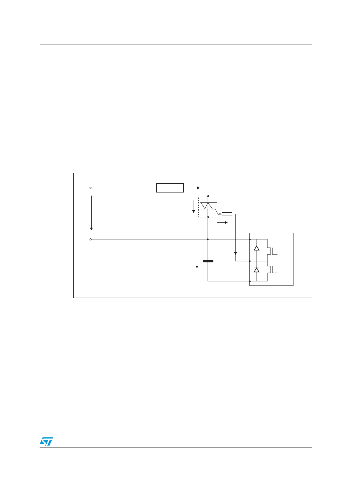
1.1 Variation of gate current with temperature
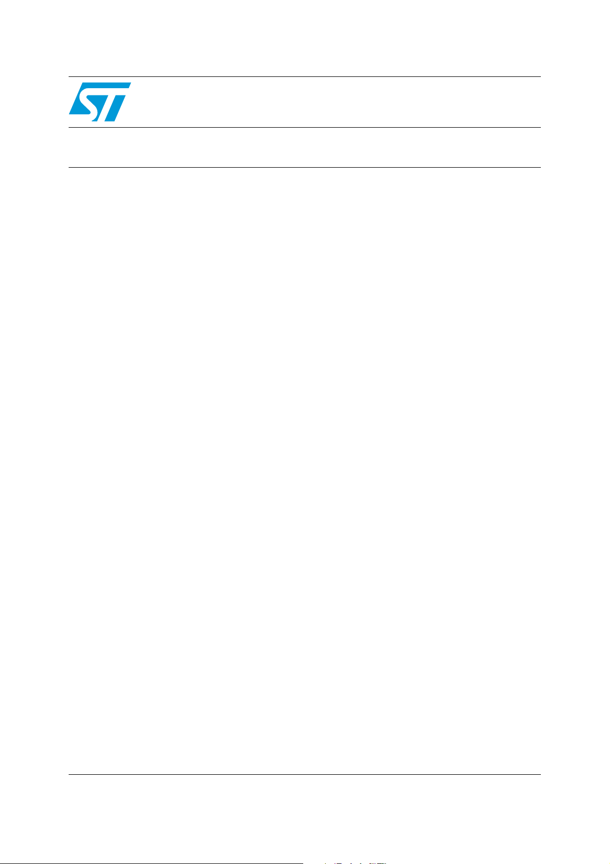
The value of the gate resistor (refer to RG in Figure 1, where a negative power supply is
used) is determined to ensure proper turn-on of the ACS™/TRIAC in the temperature range
specified by the application. The minimum gate current required for turn-on of the
ACS/TRIAC increases as the junction temperature decreases. This variation of minimum
gate current is described in the datasheet “Z01 - 1 A Triacs”, see example in Figure 2. The
worst case appears when junction temperature T
Minimum ambient temperature is set to 0 °C for most home appliance applications.
is at minimum ambient temperature.
j
The gate current (I
) level is specified for 25 °C. At temperature 0 °C this level is usually
GT
increased to a range 1.3 - 1.5 times higher for most TRIACs and AC switches.
Figure 1. Circuit for direct driving of ACS/TRIAC from MCU
Load
L
I
T
OUT/A
2
ACS/TRIAC
V
N
V
AC MAINS
T
COM/A
V
S
1
R
G
G
V
G
V
DD
I
G
D
MCU
1
M
1
+
V
D
SS
M
2
2
AM00456
Figure 1 also gives the references for the electrical parameters (VT, IT, VG) which are used in
this application note. Please note that voltage V
is referenced to the G terminal, not the A1
G
or COM terminal in order to get positive values when the current is sunk from the gate.
Doc ID 15727 Rev 1 5/18
Page 6
Gate resistor choice AN2986
Figure 2. Gate current variation with temperature for Z01 device
1.2 Resistor according to environment accuracy and variation
Temperature is not the only parameter influencing gate resistor choice. Other parameters
have also to be taken into account. Parameters discussed in this section are related to the
accuracy of the components used and to the working environment.
1.2.1 Parameters variations
All the different application parameters that have an impact on gate current level are listed
below.
Power supply voltage (V
taken into account. In appliance applications a capacitive power supply is often used. The
main part of this power supply is the Zener diode. Stability of the Zener voltage is the best at
5.1 V and 5.6 V. Accuracy of this power supply is ±10% at 5 V.
Stability of the diode at 3.3 V and 3.9 V is worse and ±0.6 V (±20%) can be achieved. This
result leads to the use of switch mode power supply (SMPS) for a 3.3 V power supply.
Output voltage levels on the I/O pins of the MCU are important variable parameters. The
most important parameter is low output level (V
when tied to ground. This parameter varies with the current flowing through this pin. The
value is given by the MCU datasheet (for example: STM8S10xxx).
) variation is one of the most important parameters that has to be
DD
) which specifies voltage on the output pin
OL
6/18 Doc ID 15727 Rev 1
Page 7

AN2986 Gate resistor choice
As an example, Tab le 1 shows data for STM8S and STM32™. The data for STM8S are
taken from the high-sink pin. The data for STM32 are taken from the GPIO pin.
Table 1. Output low level voltage (V
) for STM8S and STM32
OLmax
IG = 8 mA IG = 12 mA IG = 20 mA
STM8S (V
STM8S (V
STM32 (V
1. Maximum current capability of high-sink I/O port for STM8S with 3.3 V power supply is 12 mA as specified
in the datasheet STM8S103xx.
2. Information is not specified in the datasheet STM32103xx.
= 5 V) HS pin 0.35 V 0.6 V 1 V
DD
= 3.3 V) HS pin 0.55 V 0.9 V N/A
DD
= 3.3 V) GPIO pin 0.4 V NC
DD
It is possible to put the pins in parallel to achieve bigger current capability. In that case the
maximum current through the MCU ground pin (V
a maximum value (refer to I
VSS
STM8S103xx).
The gate resistor (R
) resistance varies with the accuracy of the resistor used. Standard
G
resistor accuracy is ±5% or ±1% with a preference for ±1% accuracy. The worst case has to
be taken into account for calculations.
The voltage drop of the gate junction (V
flowing through the TRIAC/ACS and with temperature. Its value increases with a
temperature drop at a rate of 2 mV / °C. Load current dependency is discussed in
Section 2.1.
1.2.2 Gate resistor calculation
The value of the gate resistor has to be calculated in order to deliver the proper amount of
gate current under the worst condition which are:
● minimum ambient temperature (0 °C),
● minimum supply voltage (V
● maximum voltage drop of the gate junction (V
● maximum output low voltage (V
● maximum resistance of the gate resistor for ±1% resistor accuracy (1.01 x R
The following equation summarizes all conditions for proper R
(2)
) has to be checked as it is limited to
SS
parameter on the MCU datasheet, for example:
) is a parameter that varies with the load current
GT
),
DD min
),
GTmax
) for one high-sink I/O pin of the MCU
OLmax
selection:
G
1.3 V
).
G
(1)
Equation 1
V
------------ ------------- ------------- ------------ --------- --------------
R
<
G
– V
DDminVGTmax
I
0° C()1.01×
GT
–
OLmax
Two examples of calculation are shown:
Example 1: MCU: STM8S103K2 with ACS108-6T for power supply 5 V ±10%
Specified values: I
Calculated values: I
(25 °C) = 10 mA, V
GT
(0 °C) = 1.5 x I
GT
V
= 0.9 x 5 V = 4.5 V,
DDmin
Doc ID 15727 Rev 1 7/18
= 5 V, VGT(25 °C) = 1 V
DD
(25 °C) = 15 mA,
GT
Page 8

Gate resistor choice AN2986
V
(0 °C) = 1 + 0.05 V,
GT
is then given by:
R
G
V
OLmax
[ 25 °C, I
(0 °C)] = 0.55 V
GT
Equation 2
4.5 1.05– 0.55–
------------- ------------ ------------- -----
R
G
0.015 1.01×
192Ω=<
The standard value of the resistor is 180 Ω which is also sufficient for accuracy of ±5%.
Example 2: STM32103RB + Z0103 for 3.3 V ±5%
Specified values: I
Calculated values: I
is then given by:
R
G
(25 °C)= 3 mA, VDD = 3.3 V, V
GT
(0 °C) = 1.5 x I
GT
V
V
V
= 0.95 x 3.3 V = 3.13 V,
DDmin
(0 °C) = 1.3 + 0.05 V,
GT
OLmax (IG
= 8 mA) = 0.4 V
(25 °C) = 4.5 mA,
GT
(25 °C) = 1.3 V
GT
Equation 3
3.13 1.35– 0.4–
------------- ------------ ------------- -----
R
G
0.0045 1.01×
303Ω=<
The standard value of the resistor is 300 Ω. The value 270 Ω is sufficient for accuracy of
±5%.
Please remember that we are focusing on Q2/Q3 operation (refer to AN2703 for quadrant
definition). For Q1/Q4 operation, "V
V
OHmin
. Usually V
is reached for minimum VDD.
OHmin
DDmin
– V
" in Equation 1 has to be replaced by
OLmax
Also, if a positive power supply is used (i.e. the device works in Q1/Q4 quadrants), the
required gate current is higher for Q4 operations (5 mA instead of 3 mA for other quadrants
for Z0103), and the gate resistor has to be lower than 182 Ω (R
V
DDmin
–0.4 V).
< 182 Ω for V
G
OHmin
=
8/18 Doc ID 15727 Rev 1
Page 9

AN2986 Gate current variation
2 Gate current variation
2.1 VGT variation
The voltage drop of the gate junction VGT varies with temperature and load current. The VGT
variation with temperature can be estimated as 2 mV/ °C.
variation with load current is greater and so has a higher influence on gate current
V
GT
variation. For example Figure 3 gives V
cycle for Z0103 with a 1 A 50 Hz RMS load current
The characterization of the peak value reached by the gate to A1 (or COM) voltage (refer to
"V
to "I
● V
● R
" in Figure 3) is provided when the AC switch current reaches its peak value (refer
GTpeak
"). The measurements were taken under the following conditions:
Tpeak
voltage level: 3.3 V
DD
resistance: 200 Ω for Z0103 and 100 Ω for other devices
G
With these values and using the MCU (ST7FLITE19B), the gate current (for zero-load
current) is 7.5 mA with the Z0103. This value is called "I
The V
shows that V
This V
variation with load current is larger and significant for positive half-wave. Figure 4
GT
GT
becomes negative and its value drops to –84 mV with a 1.44 A IT current.
GT
variation has a significant impact on the current consumption and cannot be
neglected. See Figure 4 and Figure 5 for graphs of V
Z0103 and ACS108-6T.
variation (dark blue curve) during an entire mains
GT
".
G0
variation versus load current for
GT
Figure 3. V
variation with load current in quadrants 2 and 3 (0.2 A RMS) for Z0103
GT
(T
= 85 °C, IG0 = 7.5 mA)
j
Doc ID 15727 Rev 1 9/18
Page 10

Gate current variation AN2986
0.6
0.7
0.8
0.9
1
–1.5 –1 –0.5 0 0.5 1 1.5
0 ˚C
85 ˚C
125 ˚C
Figure 4. Typical V
1.2
1
0.8
0.6
VGT
peak
0.4
(V)
0.2
0
–0.2
–1.5 01 –0.5 0 0.5 1 1.5
Figure 5. Typical V
VGT
peak
(V)
GTpeak
GTpeak
versus I
versus I
for Z0103 (IG0 = 7.5 mA)
Tpeak
I
(A)
Tpeak
for ACS108-6T (IG0 = 15 mA)
Tpeak
0 ˚C
85 ˚C
125 ˚C
AM00454
I
(A)
T
peak
AM00455
2.2 Minimum current calculation
The minimum gate current that is applied depends on the selection of the standard value of
the gate resistor (refer to Section 1.2.2) and the worst operating conditions.
The equation for estimating the minimum current is:
Equation 4
V
The maximum V
value has to be specified for the calculation. As Z0103 devices can be
GT
I
---------- ------------- ------------ ------------- --------- ------------ ----
<
Gmin
used with an RMS load current up to 1 A, the maximum V
current up to ±1.44 A. For ACS108-6T a maximum RMS current of 0.8 A is used.
10/18 Doc ID 15727 Rev 1
– V
DDminVGTmax
1.01 R
×
G
–
OLmax
value is taken into account for
GT
Page 11

AN2986 Gate current variation
The Z01’s maximum VGT is then close to 1.1 V at 1.44 A peak load current in negative halfwave, for a 0 °C junction temperature (worst case). A maximum value of 1.3 V is used, as
specified in the Z01 datasheet for 25 °C.
The ACS108’s maximum absolute V
is close to 1 V for a 1.15 A peak load current, for
GT
a 0 °C junction temperature (worst case). A maximum value of 1 V is used, as specified in
the ACS108-6T datasheet for 25 °C.
Two examples are shown. The same components are used as those given in Section 1.2.2.
Note that different values than those specified in Table 1 could be used, especially if a
different gate current is applied. Values are then taken from the MCU datasheet curves (for
example.: STM8S10xxx).
Example 3: MCU: STM8S with ACS108 -6T for power supply 5 V ±10%
Specified values: R
Calculated values: V
is then given by:
I
Gmin
=180 Ω, VDD = 5 V, VGT (25 °C) = 1 V
G
min= 0.9 x 5 V = 4.5 V
DD
(0 °C) = 1 + 0.05 V
V
GT
V
(25 °C, 16 mA) = 0.6 V
OLmax
Equation 5
4.5 1.05– 0.6–
Gmin
---------- ------------- ------------- ----
1.01 180×
15.7mA=<
I
The MCU is able to provide current that is above the minimum gate current for ambient
temperature 0 °C. An estimation of V
has been provided for one high-sink I/O port of
OLmax
STM8S up to 16 mA. A standard I/O port could have lower current capability (10 mA), in
which case several I/O ports have to be put in parallel.
Example 4: STM32 + Z0103 for 3.3 V ±5%
Specified values: R
Calculated values: V
V
is then given by:
I
Gmin
= 300 Ω, VDD = 3.3 V, VGT (25 °C) = 1.3 V
G
= 0.95 x 3.3 V = 3.13 V,
DDmin
(0 °C) = 0.05 + 1.3 V
V
GT
(I
OLmax
= 8 mA) = 0.4 V
GT
Equation 6
3.13 1.35– 0.4–
I
---------- ------------- ------------- -------
Gmin
1.01 300×
4.6mA=<
The MCU is able to provide current that is above the minimum gate current for ambient
temperature 0 °C. An estimation of V
(when 8 I/O ports are sunk with 8 mA each at the same time). If the current sunk by one I/O
exceeds 8 mA, the value of 1.3 V should be used instead of 0.4 V.
Doc ID 15727 Rev 1 11/18
has been provided for one I/O port of STM32
OLmax
Page 12

Gate current variation AN2986
2.3 Maximum current calculation
The maximum current that the MCU can handle is based on the following opposite
conditions:
● maximum supply voltage (V
● minimum voltage drop of the gate junction (V
● minimum gate resistor (0.99 x R
● minimum output low voltage (V
Equation 7
I
Gmax
As previously stated, a load RMS current of 1 A for Z0103 and 0.8 A for ACS108-6T is used.
),
DDmax
GTmin
),
G
).
OLmin
V
--------- ------------- ------------- ------------- -------- ------------- -- -
<
– V
DDmaxVGTmin
0.99 R
×
),
–
OLmin
G
Z01’s minimum V
is then close to –0.1 V at 1.44 A peak load current in positive half-wave
GT
and for a 125 °C junction temperature (worst case).
ACS108’s minimum V
is close to 0.6 V for 1.15 A peak load current and for a 125 °C
GT
junction temperature (worst case).
Two examples are shown. The same components are used as those given in Section 1.2.2.
Example 5: MCU: STM8S with ACS108 -6T for power supply 5 V ±10%
Specified values: R
Calculated values: V
is then given by:
I
Gmax
= 180 Ω, VDD = 5 V, VGT min (0.8 A) = 0.6 V
G
= 1.1 x 5 V = 5.5 V,
DDmax
V
OLmin IGT
= 20 mA) = 0.8 V
Equation 8
5.5 0.6– 0.8–
I
Gmax
------------ ------------- ----------- -
0.99 180×
23.2 m A=<
This result exceeds the maximum MCU current capability for one high-sink I/O port. This
I
current can be sunk with 2 I/O ports in parallel. Estimation of V
Gmax
provided for four high-sink I/O ports sinking at the same time 10 mA. V
load current. A lower load current means higher V
and therefore lower I
GTmin
OLmin
GTmin
has been
depends on
.
Gmax
Example 6: STM32 + Z0103 for 3.3 V ±5%
Specified values: R
Calculated values: V
max is then given by:
I
G
= 300 Ω, VDD = 3.3 V, VGT min = –0.1 V
G
max = 1.05 x 3.3 V = 3.47 V
DD
V
(IGT = 8 mA) = 0.4 V
OLmin
Equation 9
I
Gmax
12/18 Doc ID 15727 Rev 1
3.47 0.1–()– 0.4–
----------- ------------- ------------ ------------
0.99 300×
10.7mA=<
Page 13

AN2986 Gate current variation
The MCU is able to provide sufficient gate current. An estimation of V
provided for one I/O port of STM32 (when 8 I/O ports are sunk with 8 mA each at the same
time).
2.4 Summary of calculations
This section summarizes the calculations for devices used in Example 1 to Example 6.
ΔIG describes the difference between the maximum and minimum gate current which has
an impact on the power supply rating.
Equation 10
Average current consumption is based on the hypothesis that the maximum value is
reached continuously during the half-cycle, i.e. as if the gate current were a squared form.
The maximum average gate current is then the average of the maximum values for positive
and negative half-wave:
Equation 11
I
Gavmax
ΔIGI
–=
GmaxIGmin
1
+
---
2
I
Gmax
+()=
–
I
Gmax
OLmin
has been
where I
–
I
Equation 7, using the V
that a V
+
is the maximum gate current for positive half-wave according to Equation 7.
Gmax
is the maximum gate current for negative half-wave and is calculated according to
Gmax
of 1 V for Z0103 and 0.7 V for ACS108-6T are used for calculating the
GTmin
value estimated in Section 2.2 for negative half-wave. It means
GTmin
maximum gate current in the negative half-wave.
Table 2. Current consumption of different devices and MCUs
RG (Ω) ±1% I
STM8S + ACS108, 5 V 180 15.7 23.2
STM8S + ACS108, 3.3 V 110 15.1 20.8
STM8S + Z0103, 5 V 560 4.6 8.8 4.2 7.75
STM8S + Z0103, 3.3 V 300 4.6 9.6 5.0 7.6
STM32 + ACS108, 3.3 V 110 15.1 22.6
STM32 + Z0103, 3.3 V 300 4.6 10.7 5.7 8.85
1. This value exceeds maximum allowed current capability for one high-sink I/0 port of STM8S with 5V power
supply (20 mA). Two pins must be used instead.
2. This value exceeds maximum allowed current capability for one high-sink I/0 port of STM8S with 3.3 V
power supply (12 mA ). Two pins must be used instead.
3. This value exceeds maximum allowed current capability for one I/O port of STM32 (20 mA). Two pins must
be used instead.
Gmin
(mA) I
(mA) ΔIG (mA) I
Gmax
(1)
(2)
(3)
Gavmax
7.5 22.8
5.7 19.4
7.5 22.15
(mA)
MCUs with negative 3.3 V supply voltage can be used for triggering ACS/TRIACs, but this
puts additional constraints on the power supply design. V
30% of V
, so it is mandatory to reduce VDD ripple by precise control. For example a ±5%
DD
Doc ID 15727 Rev 1 13/18
peak variation is already around
GT
Page 14

Gate current variation AN2986
precision of power supply has been taken into account and is appropriate according to our
results. An SMPS + linear voltage regulator have to be used in order to achieve this
accuracy (example VIPER16 + LM337).
MCUs with negative 5 V power supply have some advantages concerning power supply.
Precision of ±10% is enough and can be achieved using capacitive power supply or SMPS
without additional regulation (example VIPER16, assuming a minimum output current 2
mA).
It should be noted that ACS devices are the better candidates for operation with a 3.3 V
supply as the V
GTpeak
variation is much lower than with TRIACs. Combined with a lower VDD
ripple, this helps to decrease the current consumption (maximum average gate current is
19.4 mA with 3.3 V compared to 22.8 mA with 5 V).
Placing the pins in parallel is necessary to control the 10 mA gate current AC switches with
a 3.3 V supply as the maximum gate current is 60 to 80% above the maximum allowed sunk
current for the I/O MCU pin (for example: STM8S103xx).
For a 5 V supply, the maximum calculated gate current (around 23 mA) is very close to the
maximum allowed I/O pin current. So according to application conditions (min. ambient
temperature, V
accuracy, etc.), a single pin could be used.
DD
14/18 Doc ID 15727 Rev 1
Page 15

AN2986 Proposed solutions
3 Proposed solutions
3.1 MCU current capability
The maximum current through the I/O port of the MCU can exceed the maximum current
capability of the MCU. This is a hazardous state for the MCU and has to be prevented.
There are two principal solutions. The first solution is to use a buffer transistor (refer to
Figure 6). This transistor takes over the gate current and the MCU I/O port controls only the
base with current that is 50 to 100 times lower than the ACS/TRIAC gate current.
Figure 6. Schematics of using buffer transistor
+ V
DD
+ V
DD
G
A1/COM
A2/OUT
MCUI/O
port
R6
10 K
R7
Ω
10 K
R
G
Ω
C4
10 nF
The second solution is to put the I/O ports in parallel. The maximum number of I/O ports that
can be paralled is limited by the application and MCU pin count. The maximum current must
also not exceed the maximum current capability of the MCU through the GND pin (150 mA
for STM32, 80 mA for STM8S with 3.3 V power supply or 160 mA for STM8S with 5 V power
supply).
3.2 Average current consumption
The average consumption shown in Tab le 2 is given for gate control lasting an entire period.
The consumption is in this case high. Contrary to the use of relay, it is possible to decrease
current consumption by reducing the gate pulse length which is useful when several
ACS/TRIACs are controlled at the same time (for example several small pumps or valves).
Refer to AN302 and AN303 for more information on TRIAC pulse gate control.
Load
AM00458
Doc ID 15727 Rev 1 15/18
Page 16

Conclusion AN2986
4 Conclusion
MCUs supplied from negative 3.3 V power supplies are good replacements of 5 V supplied
MCUs for the control of ACS/TRIACs.
It is possible to design gate control circuits that provide enough current for triggering the
ACS/TRIAC. Calculations of proper gate resistors have been provided.
The variation of V
The ACS devices have a lower V
has significant influence on circuit behavior for a 3.3 V power supply.
GT
variation and so are preferred for operation with a 3.3 V
GT
supply. They do indeed allow the power supply consumption to be reduced compared to
TRIACs.
The design of a 3.3 V power supply has to achieve a good accuracy (±5%) to reduce gate
current variation. A capacitive power supply cannot provide the accuracy required. An
SMPS with additional regulation has to be used.
The maximum gate current must meet MCU operating conditions. Refer to the maximum I/O
port current capability. The maximum current capability for any I/O of the STM32 port is 20
mA. One I/O pin to control the Z0103 is sufficient. Putting the I/O ports in parallel in order to
control the less sensitive devices is possible and could also be implemented.
The maximum MCU GND current capability is another parameter that has to be met. The
STM32’s current capability is 150 mA. The STM8S has different current capabilities for
different power supply ratings: 160 mA for a 5 V power supply, and 80 mA for a 3.3 V power
supply.
The average gate current consumption has to meet the capability of the power supply
current. The average gate current can be reduced using pulse gate control. This is
especially efficient for boards where several ACSs or TRIACs are controlled at the same
time.
16/18 Doc ID 15727 Rev 1
Page 17

AN2986 Revision history
5 Revision history
Table 3. Document revision history
Date Revision Changes
15-Jul-2009 1 Initial release.
Doc ID 15727 Rev 1 17/18
Page 18

AN2986
y
Please Read Carefully:
Informatio n in this document is provided solely in connection with ST products. STMicroelectronics NV and its subsidiaries (“ST”) reserve the
right to make changes, corrections, modifications or improvements, to this document, and the products and services described herein at an
time, without notice.
All ST products are sold pu rsuant to ST’s terms and conditions of sale.
Purchasers are solely responsible for the choice, selection and use of the ST products and services described herein, and ST assumes no
liability whatsoever relating to the choice, selection or use of the ST products and services described herein.
No license, express or implied, by estoppel or otherwise, to any intellectual property rights is granted under this document. If any part of this
document refers to any third party products or services it shall not be deemed a license grant by ST for the use of such third party products
or services, or any intellectual property contained therein or considered as a warranty covering the use in any manner whatsoever of such
third party products or services or any intellectual property contained therein.
UNLESS OTHERWISE SET FORTH IN ST’S TERMS AND CONDITIONS OF SALE ST DISCLAIMS ANY EXPRESS OR IMPLIED
WARRANTY WITH RESPECT TO THE USE AND/OR SALE OF ST PRODUCTS INCLUDING WITHOUT LIMITATION IMPLIED
WARRANTIES OF MERCHANTABILITY, FITNESS FOR A PARTICULAR PURPOSE (AND THEIR EQUIVALENTS UNDER THE LAWS
OF ANY JURISDICTION), OR INFRINGEMENT OF ANY PATENT, COPYRIGHT OR OTHER INTELLECTUAL PROPERTY RIGHT.
UNLESS EXPRESSLY APPROVED IN WRITING BY AN AUTHORIZED ST REPRESENTATIVE, ST PRODUCTS ARE NOT
RECOMMENDED, AUTHORIZED OR WARRANTED FOR USE IN MILITARY, AIR CRAFT, SPACE, LIFE SAVING, OR LIFE SUSTAINING
APPLICATIONS, NOR IN PRODUCTS OR SYSTEMS WHERE FAILURE OR MALFUNCTION MAY RESULT IN PERSONAL INJURY,
DEATH, OR SEVERE PROPERTY OR ENVIRONMENTAL DAMAGE. ST PRODUCTS WHICH ARE NOT SPECIFIED AS "AUTOMOTIVE
GRADE" MAY ONLY BE USED IN AUTOMOTIVE APPLICATIONS AT USER’S OWN RISK.
Resale of ST products with provisions different from the statements and/or technical features set forth in this document shall immediately void
any warranty granted by ST for the ST product or service described herein and shall not create or extend in any manner whatsoever, any
liability of ST.
ST and the ST logo are trademarks or registered trademarks of ST in various countries.
Information in this document supersedes and replaces all information previously supplied.
The ST logo is a registered trademark of STMicroelectronics. All other names are the property of their respective owners.
© 2009 STMicroelectronics - All rights reserved
STMicroelectronics group of companies
Australia - Belgium - Brazil - Canada - China - Czech Republic - Finland - France - Germany - Hong Kong - India - Israel - Italy - Japan -
Malaysia - Malta - Morocco - Philippines - Singapore - Spain - Sweden - Switzerland - United Kingdom - United States of America
www.st.com
18/18 Doc ID 15727 Rev 1
 Loading...