


AN2979
Application note
Implementing a simple ADC
using the STM8L101xx comparator
Introduction
This application note gives a simple method for implementing an A/D converter with a
minimum amount of external components: one resistor and one capacitor.
The pratical application example described in this document uses the STM8L101xx
microcontroller comparator.
February 2010 Doc ID 15651 Rev 1 1/12
www.st.com

Contents AN2979
Contents
1 Application description . . . . . . . . . . . . . . . . . . . . . . . . . . . . . . . . . . . . . . 3
1.1 Comparator features . . . . . . . . . . . . . . . . . . . . . . . . . . . . . . . . . . . . . . . . . 3
1.2 ADC implementation . . . . . . . . . . . . . . . . . . . . . . . . . . . . . . . . . . . . . . . . . 3
2 Software description . . . . . . . . . . . . . . . . . . . . . . . . . . . . . . . . . . . . . . . . . 5
2.1 Application flowcharts . . . . . . . . . . . . . . . . . . . . . . . . . . . . . . . . . . . . . . . . 6
3 Hardware description . . . . . . . . . . . . . . . . . . . . . . . . . . . . . . . . . . . . . . . . 7
4 Measurements and calibration . . . . . . . . . . . . . . . . . . . . . . . . . . . . . . . . . 8
4.1 Typical measurements . . . . . . . . . . . . . . . . . . . . . . . . . . . . . . . . . . . . . . . . 8
4.2 Precision of the measured value . . . . . . . . . . . . . . . . . . . . . . . . . . . . . . . . 8
4.3 How to get a better accuracy . . . . . . . . . . . . . . . . . . . . . . . . . . . . . . . . . . . 9
4.3.1 Hardware solution . . . . . . . . . . . . . . . . . . . . . . . . . . . . . . . . . . . . . . . . . . 9
4.3.2 Software solution . . . . . . . . . . . . . . . . . . . . . . . . . . . . . . . . . . . . . . . . . . . 9
5 Revision history . . . . . . . . . . . . . . . . . . . . . . . . . . . . . . . . . . . . . . . . . . . 11
2/12 Doc ID 15651 Rev 1

AN2979 Application description
V
meas
V
DD
1
t
T
---–
⎝⎠
⎛⎞
exp–
⎝⎠
⎛⎞
×=
1 Application description
1.1 Comparator features
The STM8L101xx microcontroller embeds two zero-crossing comparators sharing the same
current bias and the same voltage reference.
This voltage reference can be:
● internal (comparison to ground)
● or external (comparison to a reference pin voltage)
Each comparator is connected to 4 channels which can be used to generate an interrupt, a
timer input capture or a timer break. Their polarity can be inverted.
Note: For external comparison be aware that the STM8L101xx comparator maximum input value
is V
-1.25 V with V
DD
1.2 ADC implementation
Each comparator can be used to implement an ADC. This technique is based on a simple
principle: the signal to be measured is connected to the non-inverted input and the
reference signal is an external signal connected to the inverting input.
DDmax
= 3.6 V
In the demonstration software, the comparator used is COMP2 and the channel used as the
signal to be measured is the channel 3 (pin PD2).
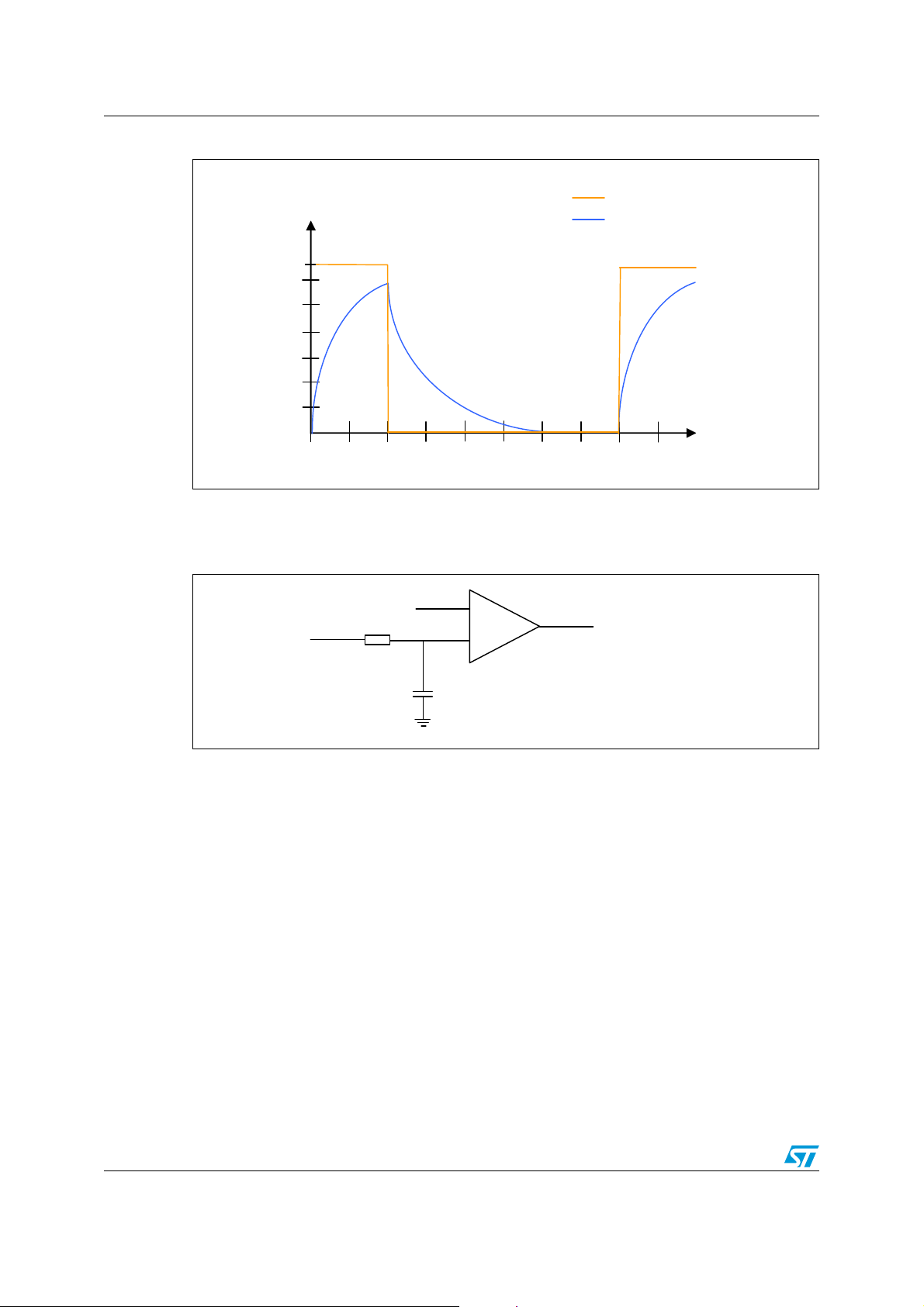
The reference signal is generated by charging a capacitor through a resistor. While the
voltage across the capacitor is being charged, it follows an exponential curve.
This exponential equation has been implemented in the software. The time taken by the
capacitor voltage to rise above the voltage value to be converted is used in the charge
equation to retrieve the digital conversion value.
Charge equation:
Where:
● Vmeas is the value to be mesaured
● V
● t is the time measured by timer2 when the comparator detects that the input voltage is
is the input voltage
DD
above the reference voltage
● T is the RC constant (here R=10 kΩ and C=100 nF so T= 1 ms)
The capacitor is charged and discharged using the timer 2 PWM on channel1/ PB0.
A timer is programmed to generate a 2 ms PWM with a duty cycle of 0.25. This 2-ms period
permits an ADC implementation using the full voltage range that the comparator tolerates.
The capacitor charging curve is shown in the following figure.
Doc ID 15651 Rev 1 3/12
Application description AN2979
PWM output
Capacitor charging curve
V
DD
T(ms)
3.3
2.5
2
1.5
1
0.5
123456789
(V)
3
AI
-
+
C=100 nF
PB0/PC4
PA6
PD2
COMP_OUT
R=10 k7
Figure 1. Capacitor charging curve
The figure below shows the connection of the comparator to the required external
components.
Figure 2. Comparator connections
1. Condition: VDD=3.3 V, R=10 kΩ, C=100 nF
Note: When using the STM8L101-EVAL evaluation board you need to connect the PB0 pin to the
PC4 pin. This way you use the resistor and capacitor already present on the board (no
hardware needed). Pin PC4 is configured as input floating to avoid any conflict.
4/12 Doc ID 15651 Rev 1
 Loading...