

Page 1
AN2970
1
1
ai15544
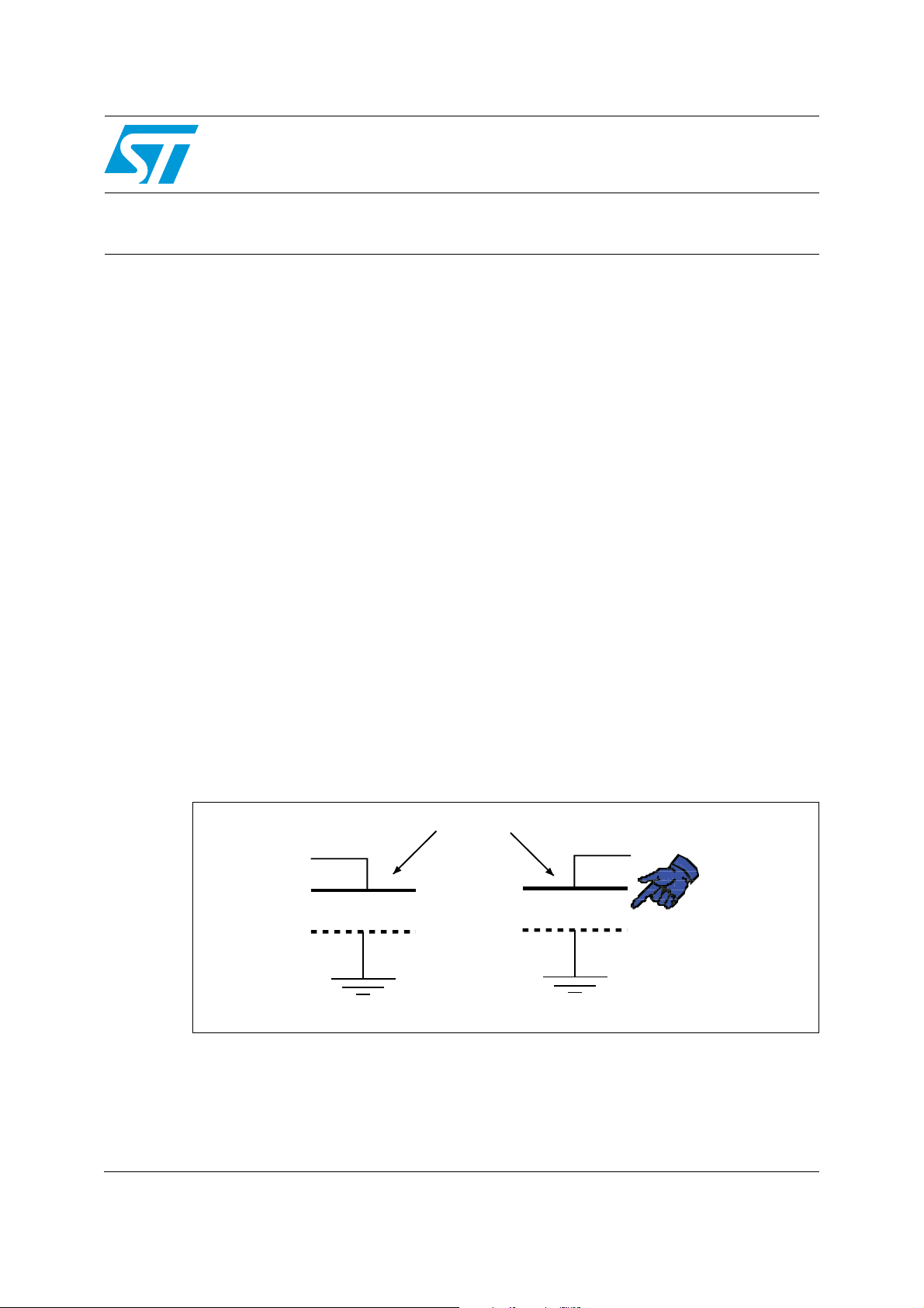
Sensing electrode
Application note
Principles of capacitive touch and proximity sensing technology
The objective of this document is to present the principles of capacitive sensing and charge
transfer used in STMicroelectronics STM8T and STM8TS capacitive sensors. All devices
can be configured in touch or proximity sensing.
1 Capacitive sensing overview
1.1 Sensing electrode capacitance
A capacitance exists between any reference point relative to ground as long as they are
electrically isolated. If this reference point is a sensing electrode, it helps to think of it as a
capacitor. The positive electrode of the capacitor is the sensing electrode, and the negative
electrode is formed by the surrounding area (virtual ground reference, labelled 1 in
Figure 1).
When a conductive object is brought into proximity of the sensing electrode, the coupling
between the object and the electrode increases, together with the capacitance of the
sensing electrode relative to ground. For example, a human hand will increase the sensing
electrode capacitance as it approaches it. Touching the dielectric panel that protects the
electrode increases its capacitance significantly.
The sensing electrode can be made of any electrically conductive material, such as copper
on PCBs, or transparent conductive material like Indium Tin Oxide (ITO) deposited on glass
or Plexiglas.
Figure 1. Coupling with hand increases the capacitance of the sensing electrode
May 2009 DocID 15625 Rev 1 1/8
www.st.com
Page 2
Capacitive sensing overview AN2970
1.2 Principles of charge transfer
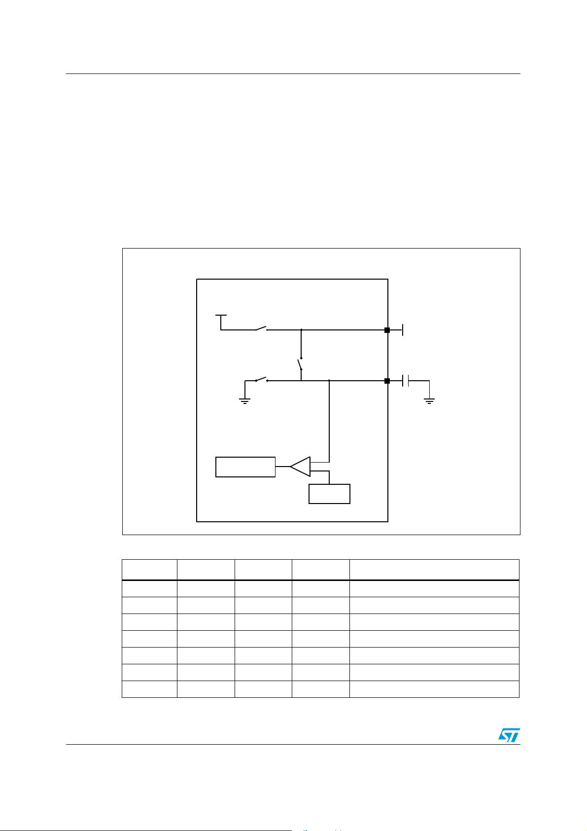
The sensing electrode is connected to the CX pin of the STM8T or STM8TS device. The
equivalent capacitance of the sensing electrode is referred to as C
C
is fully charged with a stable reference voltage VDD. The charge on CX is transferred to a
X
reference capacitor (C
C
. The process is repeated until the voltage on CS reaches a threshold (approximately
X
20% of V
). This threshold is referred to as V
DD
to reach the threshold represents the size of C
). CS capacitance is typically from 1000 to 100,000 times bigger than
S
. The number of transfer cycles required
TRIP
. Refer to Figure 3 and Ta bl e 1 for a
X
representation of the charge-transfer equivalent hardware and charge-transfer sequence for
a given channel.
Figure 2. Depiction of channel charge-transfer hardware
34-443CAPACITIVESENSINGBLOCK
.
X
3TABLE6
$$
3
3
3
#8
3ENSINGELECTRODE
2EFERENCE
#APACITOR
#S
42)0
'%.%2!4%$
3TABLE
REFERENCE
Table 1. Charge transfer sequence
(1)
Step Switch S3 Switch S2 Switch S1 Description
11 0 1 C
2 0 0 0 Deadtime
BJ
discharge
S
3 0 1 0 Charge cycle (CX charge)
4 0 0 0 Deadtime
5 0 0 1 Transfer cycle (charge transferred to C
6 0 0 0 Deadtime
71 0 1 C
1. Step 2 to 7 are repeated until the voltage across C
2/8 DocID 15625 Rev 1
reaches V
S
TRIP
threshold.
discharge
X
)
S
Page 3
AN2970 Capacitive sensing overview
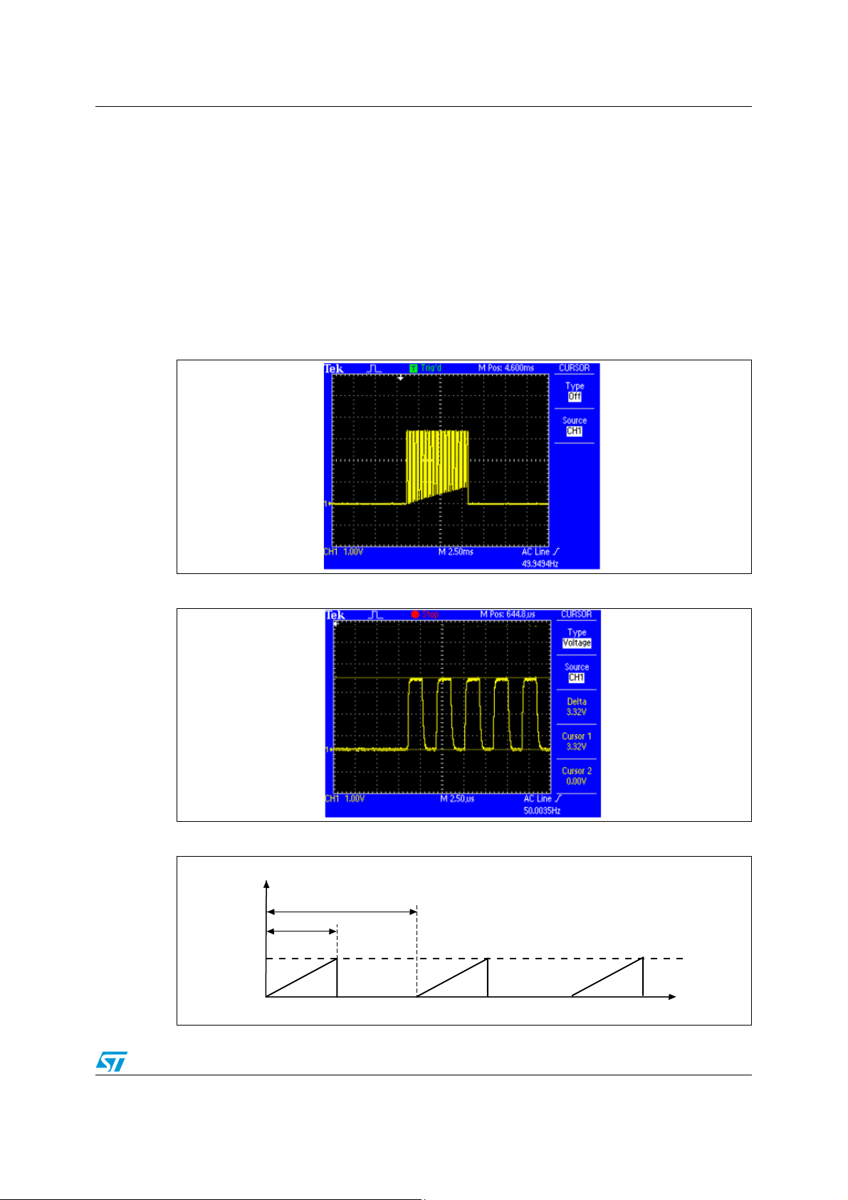
T
#HARGECYCLEDURATION
!I
6
42)0
#3PINVOLTAGE
3AMPLINGPERIOD
Figure 3 and Figure 4 show the evolution of the CX voltage during one and five charge
transfer sequences, respectively. The transfer cycle refers to the charging of C
transfer of the charge to the C
C
to V
S
using a sequence of transfer cycles. The charge cycle duration refers to the time
TRIP
needed to complete one C
capacitor. The charge cycle refers to process of charging
S
charge cycle when no proximity or touch (thus the longest
S
and the
X
duration of a charge cycle with the current system parameters). The charge cycles can be
probed from the CS pin. It is graphically illustrated in Figure 5. Refer to Section 1.4: C
capacitor for details on how to select C
capacitors.
S
S
In addition, the devices can compensate to environmental changes by tracking the average
capacitance of the sensing electrode. This average value is compared to the latest charge
cycle to determine whether a proximity or touch occurred.
Figure 3. Voltage across C
Figure 4. Voltage across C
over a full charge transfer sequence
X
over the first 5 charge transfers
X
Figure 5. Charge cycle
DocID 15625 Rev 1 3/8
Page 4

Capacitive sensing overview AN2970
1.3 Transfer rate
The transfer cycles can be performed at a default rate depending on the internal oscillator
frequency. According to the device, this frequency can be modified either through OTP
option bytes or by the application software. It is recommended to modify the oscillator
frequency for advanced designs only.
The oscillator is used to determine the rate at which the charge transfers is performed. A
maximum efficiency is achieved when enough time is allowed to fully charge C
completely transfer this charge to the C
capacitor.
S
A transfer rate between 100 kHz and 150 kHz is a good choice in normal operating
conditions. The default transfer rate is in this range.
to VDD and
X
A serial resistor R
connected to the CX pin negatively influences the transfer cycle. This
X
resistor improves the conductive object electrical isolation from the sensing electrode and
provides additional ESD protection for the device. Typical R
value ranges from 1 to 2kΩ.
X
Figure 4 and Figure 6 show ideal charge cycles probed from the CX pin. In Figure 4, it can
be noted that the sensing electrode charges up to V
V
is reached.
TRIP
, and that the charge cycle halts when
DD
Figure 6. Ideal charge transfers
Figure 7 and Figure 8 shows non-ideal charge transfers and the resulting charge cycle.
It can be noted that the sensing electrode is charged up to 2.12 V instead of V
DD
comparing Figure 8 to Figure 6, it can be noted that the offset is due to the fact that a
fraction of the sensing electrode charge is not transferred to the C
corrected by decreasing either the transfer rate (oscillator frequency) or R
capacitor. This can be
S
.
X
Note: Attaching a probe to the sensing electrode increases the sensing electrode capacitance by
a few picoFarads, depending on the probe. This has an instant negative influence on the
sensitivity of the system. After a short period of time, the system automatically adjusts to
compensate this change.
4/8 DocID 15625 Rev 1
. By
Page 5

AN2970 Capacitive sensing overview
Figure 7. Non-ideal charge transfers
Figure 8. Charge cycle resulting from non-ideal charge transfers
DocID 15625 Rev 1 5/8
Page 6

Capacitive sensing overview AN2970
1.4 CS capacitor
The function of the CS capacitor is to collect the charge from the sensing electrode. It also
influences the sensitivity of the system. A bigger C
capacitance is computed with a higher resolution. This will increase the sensitivity of the
device.
When the STM8T and STM8TS device is powered from an AC supply voltage, the charge
cycle is always synchronized with the positive zero crossings (ZC) of the AC voltage. The
charge cycle starts after the zero crossing when the device is ready. The ZC feature is not
available on all devices.
When the device is powered from a DC supply voltage, most devices generate an internal
50 Hz sampling frequency (f
SAMPLING
) and synchronize the charge cycles with this
frequency (see Section 1.3: Transfer rate).
capacitor will ensure that the CX
S
The minimum and maximum charge cycle duration (t
SAMPLING
) is determined by the
following:
● Minimum charge cycle duration: every charge cycle must consist of at least 32 charge
transfers.
● Maximum charge cycle duration: no more than 214 charge transfers are allowed in a
charge cycle.
A larger sensing electrode surface will require a larger C
the C
capacitance is normally unknown, it is easier to design the CS capacitor using a trial-
X
and-error method. The C
capacitor typically ranges from 10 nF to 1 µF.
S
capacitor and vice versa. Since
S
It can be noted that the bigger the sensing electrode, the more likely it is for noise to couple
into the system. This could influence the sensitivity setting chosen for the device.
6/8 DocID 15625 Rev 1
Page 7

AN2970 Revision history
2 Revision history
Table 2. Document revision history
Date Revision Changes
04-May-2009 1 Initial release.
DocID 15625 Rev 1 7/8
Page 8

AN2970
Please Read Carefully:
Information in this document is provided solely in connection with ST products. STMicroelectronics NV and its subsidiaries (“ST”) reserve the
right to make changes, corrections, modifications or improvements, to this document, and the products and services described herein at any
time, without notice.
All ST products are sold pursuant to ST’s terms and conditions of sale.
Purchasers are solely responsible for the choice, selection and use of the ST products and services described herein, and ST assumes no
liability whatsoever relating to the choice, selection or use of the ST products and services described herein.
No license, express or implied, by estoppel or otherwise, to any intellectual property rights is granted under this document. If any part of this
document refers to any third party products or services it shall not be deemed a license grant by ST for the use of such third party products
or services, or any intellectual property contained therein or considered as a warranty covering the use in any manner whatsoever of such
third party products or services or any intellectual property contained therein.
UNLESS OTHERWISE SET FORTH IN ST’S TERMS AND CONDITIONS OF SALE ST DISCLAIMS ANY EXPRESS OR IMPLIED
WARRANTY WITH RESPECT TO THE USE AND/OR SALE OF ST PRODUCTS INCLUDING WITHOUT LIMITATION IMPLIED
WARRANTIES OF MERCHANTABILITY, FITNESS FOR A PARTICULAR PURPOSE (AND THEIR EQUIVALENTS UNDER THE LAWS
OF ANY JURISDICTION), OR INFRINGEMENT OF ANY PATENT, COPYRIGHT OR OTHER INTELLECTUAL PROPERTY RIGHT.
UNLESS EXPRESSLY APPROVED IN WRITING BY AN AUTHORIZED ST REPRESENTATIVE, ST PRODUCTS ARE NOT
RECOMMENDED, AUTHORIZED OR WARRANTED FOR USE IN MILITARY, AIR CRAFT, SPACE, LIFE SAVING, OR LIFE SUSTAINING
APPLICATIONS, NOR IN PRODUCTS OR SYSTEMS WHERE FAILURE OR MALFUNCTION MAY RESULT IN PERSONAL INJURY,
DEATH, OR SEVERE PROPERTY OR ENVIRONMENTAL DAMAGE. ST PRODUCTS WHICH ARE NOT SPECIFIED AS "AUTOMOTIVE
GRADE" MAY ONLY BE USED IN AUTOMOTIVE APPLICATIONS AT USER’S OWN RISK.
Resale of ST products with provisions different from the statements and/or technical features set forth in this document shall immediately void
any warranty granted by ST for the ST product or service described herein and shall not create or extend in any manner whatsoever, any
liability of ST.
ST and the ST logo are trademarks or registered trademarks of ST in various countries.
Information in this document supersedes and replaces all information previously supplied.
The ST logo is a registered trademark of STMicroelectronics. All other names are the property of their respective owners.
© 2009 STMicroelectronics - All rights reserved
STMicroelectronics group of companies
Australia - Belgium - Brazil - Canada - China - Czech Republic - Finland - France - Germany - Hong Kong - India - Israel - Italy - Japan -
Malaysia - Malta - Morocco - Philippines - Singapore - Spain - Sweden - Switzerland - United Kingdom - United States of America
www.st.com
8/8 DocID 15625 Rev 1
 Loading...