

AN2936
Application note
10 W SMPS with HV power MOSFET and the L6565
for three-phase industrial applications
Introduction
This document introduces a solution for industrial power supplies fed by a three-phase
mains. It uses a high voltage power MOSFET with 1500 V breakdown voltage to optimize
the operation of a quasi-resonant flyback converter based on the primary controller L6565.
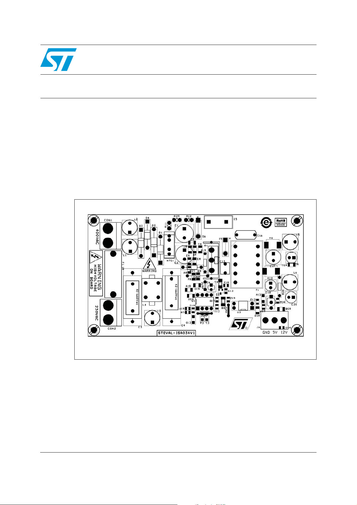
The STEVAL-ISA034V1 demonstration board has been designed and developed for low
power applications. The board features two isolated outputs, 12 V and 5 V, and is capable of
delivering up to 10 W.
The board can be ordered through order code STEVAL-ISA034V1.
Figure 1. 10 W board prototype
AM01332v1
March 2009 Rev 1 1/10
www.st.com

Contents AN2936
Contents
1 Demonstration board description . . . . . . . . . . . . . . . . . . . . . . . . . . . . . . 3
1.1 Bill of materials . . . . . . . . . . . . . . . . . . . . . . . . . . . . . . . . . . . . . . . . . . . . . . 6
2 Related documents . . . . . . . . . . . . . . . . . . . . . . . . . . . . . . . . . . . . . . . . . . 9
3 Revision history . . . . . . . . . . . . . . . . . . . . . . . . . . . . . . . . . . . . . . . . . . . . 9
2/10
AN2936 Demonstration board description
1 Demonstration board description
The STEVAL-ISA034V1 demonstration board is based on a quasi-resonant flyback
converter topology and uses the STP3N150 1500 V power MOSFET as the primary switch.
The STP3N150 employs STMicroelectronics’ proprietary high voltage Mesh Overlay
technology. Characteristic of this technology, the switch features very low R
low gate charge and high switching performance. The device is available in the TO-220, TO247 and TO-220FH packages.
The demonstration board is designed in accordance with the specifications in Ta b l e 1 .
Table 1. Main specifications
Parameter Value
Input voltage range 185 to 460 Vac
Input frequency range 50/60 Hz
Output 1 12 V @ 0.6 A
Output 2 5 V @ 0.55 A
Output power 10 W
DS(on)
per area,
Safety EN60950
EMI EN55014
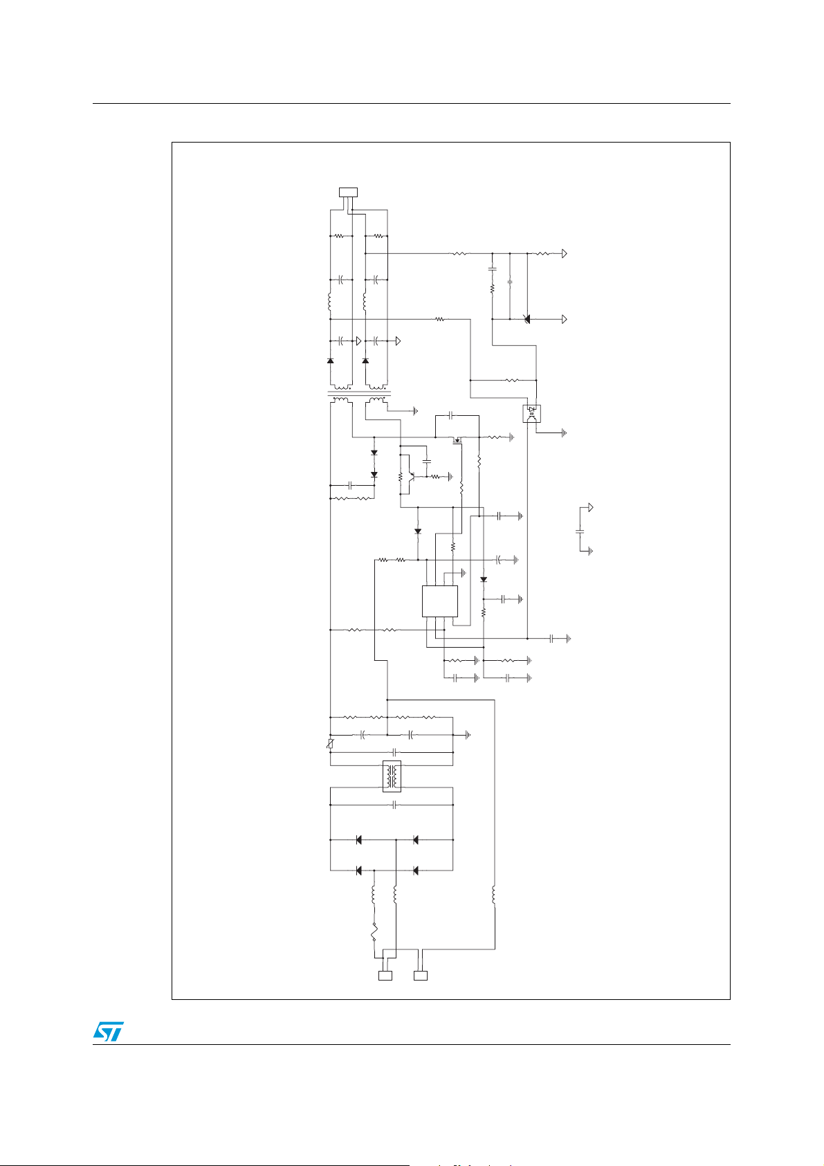
The input section is equipped with two connectors: CON1 for 400 Vac input voltage, and
CON2 for 230 Vac input voltage. The output voltages are available on CON3, with a shared
ground between the two outputs.
The converter is controlled by the L6565, a primary controller for quasi-resonant ZVS (zerovoltage switching) flyback converters. The device is capable of controlling power variations
in the mains voltage by means of line voltage feed-forward. In light load conditions the
device features a special function which automatically lowers the operating frequency while
maintaining operation as close to ZVS as possible. In addition to very low startup and
quiescent currents, this feature helps to maintain low consumption from the mains in light
load conditions.
The device also includes a disable function, an on-chip filter on current sense, an error
amplifier with a precise reference voltage for primary regulation and effective two-level
overcurrent protection. The transformer reflected voltage is set to 400 V, providing enough
margin for leakage inductance voltage spikes. A small RCD clamper circuit is used to limit
excess voltage on the drain of the power MOSFET. During normal operation, the L6565 is
powered by the auxiliary winding of the transformer, via diode D7. A spike killer circuit for the
auxiliary voltage fluctuations is present, but not connected (Q2, C12, R15). The primary
current is measured using an external sensing resistor (R21) for current mode operation.
Output voltage regulation is performed using secondary feedback on the 5 V output.
The feedback network consists of a programmable voltage reference, TL431, driving an
optocoupler which ensures the required insulation between the primary and secondary
sections. The optotransistor drives the feedback pin (COMP), which controls the operation
of the device. LC filters have been added on both of the outputs to reduce the high
frequency ripple, using moderate output capacitor values.
3/10

Demonstration board description AN2936
The flyback transformer is a layer-type based on an E25/13/7 core and N27 ferrite,
manufactured by Tronic, and ensures safety insulation in accordance with standard
EN60950. The schematic of the board is shown in Figure 2. The power supply has been
built on a double-sided 35 µm PCB in FR-4, size 120 x 68 mm. The bill of material is
provided in Ta b l e 3 .
4/10
AN2936 Demonstration board description
Figure 2. Circuit schematic
12V @ 600 mA
5V @ 550 mA
J6
CON2
2
3
1
R24
nc
R25
nc
R22
R21
10k
C17
Co3
Co4
22u - 25V
22u - 10V
L6
D8
8
T1
1
10u
L7
10u
Co2
Co1
220u - 25V
220u - 10V
D9
STPS3L40S
STPS3L25S
7
2543 6
C8
R9
150K
TRANSFORMER
D5
STTH108
D4
R11
1n/2kV
STTH108
R10
150K
R19
2.2k
N1/N5V=87
Lp=15mH
N1/N12V=38
N1/Naux=30
Core material N67
Core shape E20 (E25)
nc
C16
M1
12
6.8n - nc
C15
2.2k - nc
R12
10
Q11 nc
R16
330n
C18
560
R23
R18
3.5
STP4N150
3
1k
R17
2.2
100p
C14
10k
n.c.
1
3
2
U3
TL431
R20
1k
U2
PC817
D6
1N4148
R7
330k
R8
330k
R5
1.8M
R6
1.8M
R26
1M
R27
1M
C22
NTC2
50E
D13
480-650VDC
D12
R281MR29
+
1N4007
1N4007
C23
4.7uF
10n-X2
C21
2 3
L11
1
4
C20
10n-X2
A C
A C
L8 1mH
L9 1mH
R15
8
5
7
6
GD
ZCD
VCC
GND
U1
VFF
INV
COMP2CS
3
1
4
R12
C10
1M
+
4.7uF
27 mH
D10
1N4007
A C
D11
1N4007
A C
C9
15k
12k
1n
47u
D7
1N4148
100n
C13
L6565
120k
R14
R13
27k
2.2n
C11
L10 1 mH
C19
2.2n - Y1
220p
C12
F4 1A
1
2
1
2
400Vac
CON2
CON1
230Vac
AM01331v1
5/10

Demonstration board description AN2936
1.1 Bill of materials
Table 2. Bill of materials
Reference Value Description
C1 4.7 µF - 450 V Elect. capacitor
C2 4.7 µF - 450 V Elect. capacitor
C3 10 nF - 660 V Polip. capacitor X2
C4 10 nF - 660 V Polip. capacitor X2
C5 1 nF - 2 kV Polip. capacitor FKP
C6 47 µF - 50 V Elec. capacitor
C7 1 nF - 50 V Ceramic capacitor
C8 2.2 nF Ceramic capacitor
C9 220 pF Ceramic capacitor
C10 100 nF Ceramic capacitor
C11 100 pF Ceramic capacitor
C12 n.m. Ceramic capacitor
C13 n.m. Ceramic capacitor
C14 330 nF Ceramic capacitor
C15 n.m. Ceramic capacitor
C16 2.2 nF Ceramic capacitor Y1
C17 220 µF – 25 V Elec. capacitor 85 °C
C18 220 µF – 16 V Elec. capacitor 85 °C
C19 22 µF- 25 V Elec. capacitor
C20 22 µF- 25 V Elec. capacitor
D1, D2, D3, D4 1N4007 Rectifier 1000 V 1 A
D5 STTH108 Turboswitch diode 1 A-800 V - STMicroelectronics
D6 STTH108 Turboswitch diode 1 A-800 V - STMicroelectronics
D7 LL4148/SOD-80 SOD-80 general-purpose rectifier 75 V 200 mA
D8 LL4148/SOD-80 SOD-80 general-purpose rectifier 75 V 200 mA
D9 STPS3L40S Schottky rectifier 3 A-40 V
D10 STPS3L25S Schottky rectifier 3 A-25 V
L1, L2, L3 1 mH
L4 33 mH Common mode choke
L5 10 µH Inductor
L6 10 µH Inductor
NTC1 50 Ω NTC inrush current suppressor
F1 1 A Fuse
6/10
AN2936 Demonstration board description
Table 2. Bill of materials (continued)
Reference Value Description
R1 1 mΩ Resistor, metal film 0.25 W 5%, SMD
R2 1 mΩ Resistor, metal film 0.25 W 5%, SMD
R3 1 mΩ Resistor, metal film 0.25 W 5%, SMD
R4 1 mΩ Resistor, metal film 0.25 W 5%, SMD
R5 1.8 mΩ Resistor, metal film 0.25 W 5%, SMD
R6 1.8 mΩ Resistor, metal film 0.25 W 5%, SMD
R7 1.8 mΩ Resistor, metal film 0.25 W 5%, SMD
R8 1.8 mΩ Resistor, metal film 0.25 W 5%, SMD
R9 330 kΩ Resistor, metal film 0.25 W 5%, SMD
R10 330 kΩ Resistor, metal film 0.25 W 5%, SMD
R11 150 kΩ Resistor, metal film 0.25 W 5%, SMD
R12 150 kΩ Resistor, metal film 0.25 W 5%, SMD
R13 10 Ω
R14 12 kΩ Resistor, metal film 0.25 W 5%, SMD
R15 2.2 kΩ – n.m. Resistor, metal film 0.25 W 5%, SMD
R16 18 kΩ Resistor, metal film 0.25 W 5%, SMD
R17 120 kΩ Resistor, metal film 0.25 W 5%, SMD
R18 15 kΩ
R19 2.2 Ω
R20 1 kΩ
R21 3.5 Ω
R22 2.2 kΩ
R23 1 kΩ
R24 10 kΩ
R25 10 kΩ
R26 560 Ω
R27 n.m.
R28 n.m.
R29 150 kΩ Resistor, metal film 0.25 W 5%, SMD
R30 1.2 kΩ
T1 0603261 Switch mode transformer - Tronic
U1 L6565 Quasi resonant controller - STMicroelectronics
U2 PC817 Optocoupler
U3 TL431 Programmable shunt voltage reference 1% - STMicroelectronics
7/10

Demonstration board description AN2936
Table 2. Bill of materials (continued)
Reference Value Description
Q1 STP3N150 Power MOSFET 1500 V - 3 A - STMicroelectronics
Q2 BC547 Small signal PNP transistor
8/10
AN2936 Related documents
2 Related documents
1. AN1326: L6565 quasi-resonant controller
3 Revision history
Table 3. Document revision history
Date Revision Changes
16-Mar-2009 1 Initial release.
9/10

AN2936
Please Read Carefully:
Information in this document is provided solely in connection with ST products. STMicroelectronics NV and its subsidiaries (“ST”) reserve the
right to make changes, corrections, modifications or improvements, to this document, and the products and services described herein at any
time, without notice.
All ST products are sold pursuant to ST’s terms and conditions of sale.
Purchasers are solely responsible for the choice, selection and use of the ST products and services described herein, and ST assumes no
liability whatsoever relating to the choice, selection or use of the ST products and services described herein.
No license, express or implied, by estoppel or otherwise, to any intellectual property rights is granted under this document. If any part of this
document refers to any third party products or services it shall not be deemed a license grant by ST for the use of such third party products
or services, or any intellectual property contained therein or considered as a warranty covering the use in any manner whatsoever of such
third party products or services or any intellectual property contained therein.
UNLESS OTHERWISE SET FORTH IN ST’S TERMS AND CONDITIONS OF SALE ST DISCLAIMS ANY EXPRESS OR IMPLIED
WARRANTY WITH RESPECT TO THE USE AND/OR SALE OF ST PRODUCTS INCLUDING WITHOUT LIMITATION IMPLIED
WARRANTIES OF MERCHANTABILITY, FITNESS FOR A PARTICULAR PURPOSE (AND THEIR EQUIVALENTS UNDER THE LAWS
OF ANY JURISDICTION), OR INFRINGEMENT OF ANY PATENT, COPYRIGHT OR OTHER INTELLECTUAL PROPERTY RIGHT.
UNLESS EXPRESSLY APPROVED IN WRITING BY AN AUTHORIZED ST REPRESENTATIVE, ST PRODUCTS ARE NOT
RECOMMENDED, AUTHORIZED OR WARRANTED FOR USE IN MILITARY, AIR CRAFT, SPACE, LIFE SAVING, OR LIFE SUSTAINING
APPLICATIONS, NOR IN PRODUCTS OR SYSTEMS WHERE FAILURE OR MALFUNCTION MAY RESULT IN PERSONAL INJURY,
DEATH, OR SEVERE PROPERTY OR ENVIRONMENTAL DAMAGE. ST PRODUCTS WHICH ARE NOT SPECIFIED AS "AUTOMOTIVE
GRADE" MAY ONLY BE USED IN AUTOMOTIVE APPLICATIONS AT USER’S OWN RISK.
Resale of ST products with provisions different from the statements and/or technical features set forth in this document shall immediately void
any warranty granted by ST for the ST product or service described herein and shall not create or extend in any manner whatsoever, any
liability of ST.
ST and the ST logo are trademarks or registered trademarks of ST in various countries.
Information in this document supersedes and replaces all information previously supplied.
The ST logo is a registered trademark of STMicroelectronics. All other names are the property of their respective owners.
© 2009 STMicroelectronics - All rights reserved
STMicroelectronics group of companies
Australia - Belgium - Brazil - Canada - China - Czech Republic - Finland - France - Germany - Hong Kong - India - Israel - Italy - Japan -
Malaysia - Malta - Morocco - Singapore - Spain - Sweden - Switzerland - United Kingdom - United States of America
www.st.com
10/10
 Loading...