

Page 1

AN2933
Application note
Demo board user guidelines for the TS4999 filter-free stereo
2 x 2.8 W class D audio power amplifier with selectable 3D effect
Introduction
This application note concerns the TS4999 demonstration board, designed to evaluate the
stereo class D audio differential amplifier TS4999.
This document provides:
■ a brief description of the TS4999 device.
■ a description of the demonstration board and all of its components.
■ the layout of the demonstration board.
About the TS4999
The TS4999 is a fully-differential class D stereo power amplifier. It can drive up to 1.35 W
into an 8 Ω load at 5 V per channel. The device has four different gain settings utilizing two
discrete pins, G0 and G1.
Pop and click reduction circuitry provides low on/off switch noise while allowing the device to
start within 8 ms. 3D enhancement effects are selected through one digital input pin that
allows more amazing stereo audio sound.
Two standby pins (active low) allow each channel to be switched off separately.
The TS4999 is available in an 18-bump flip-chip package.
Key features of the TS4999
■ Operating range from V
■ Dedicated standby mode active low for each channel.
■ Output power per channel: 2.8 W at 5 V into 4 Ω with 10% THD+N or 0.7 W at 3.6 V into
8 Ω with 1% THD+N max.
■ Selectable 3D sound effect.
■ Four gain setting steps: 3.5, 6, 9.5 and 12 dB.
■ Low current consumption.
■ PSRR: 63 dB typical at 217 Hz.
■ Fast start-up phase: 7.8 ms.
■ Output short-circuit and thermal shutdown protection.
■ Flip-chip 18-bump lead-free package.
Refer to the datasheet for complete information on the TS4999.
= 2.4 V to 5.5 V.
CC
March 2009 Rev 1 1/10
www.st.com
Page 2
Description of the demonstration board AN2933
1 Description of the demonstration board
The TS4999 demonstration board is designed to evaluate the TS4999, a fully-differential
class D stereo power amplifier. The TS4999 device, in a flip-chip package, is mounted on a
four-layer PCB. Easily-accessible connectors on the board allow changing or driving the
gain select pins (G0 and G1), the standby control pins for the left and right channels (STBL
and STBR) and the 3D sound effect pin (3D).
The differential gain of the TS4999 can be set to 3.5, 6, 9.5, or 12 dB, depending on the
logic level of the G0 pin (connected to pin 2 of S1) and G1 pin (connected to pin 2 of S2).
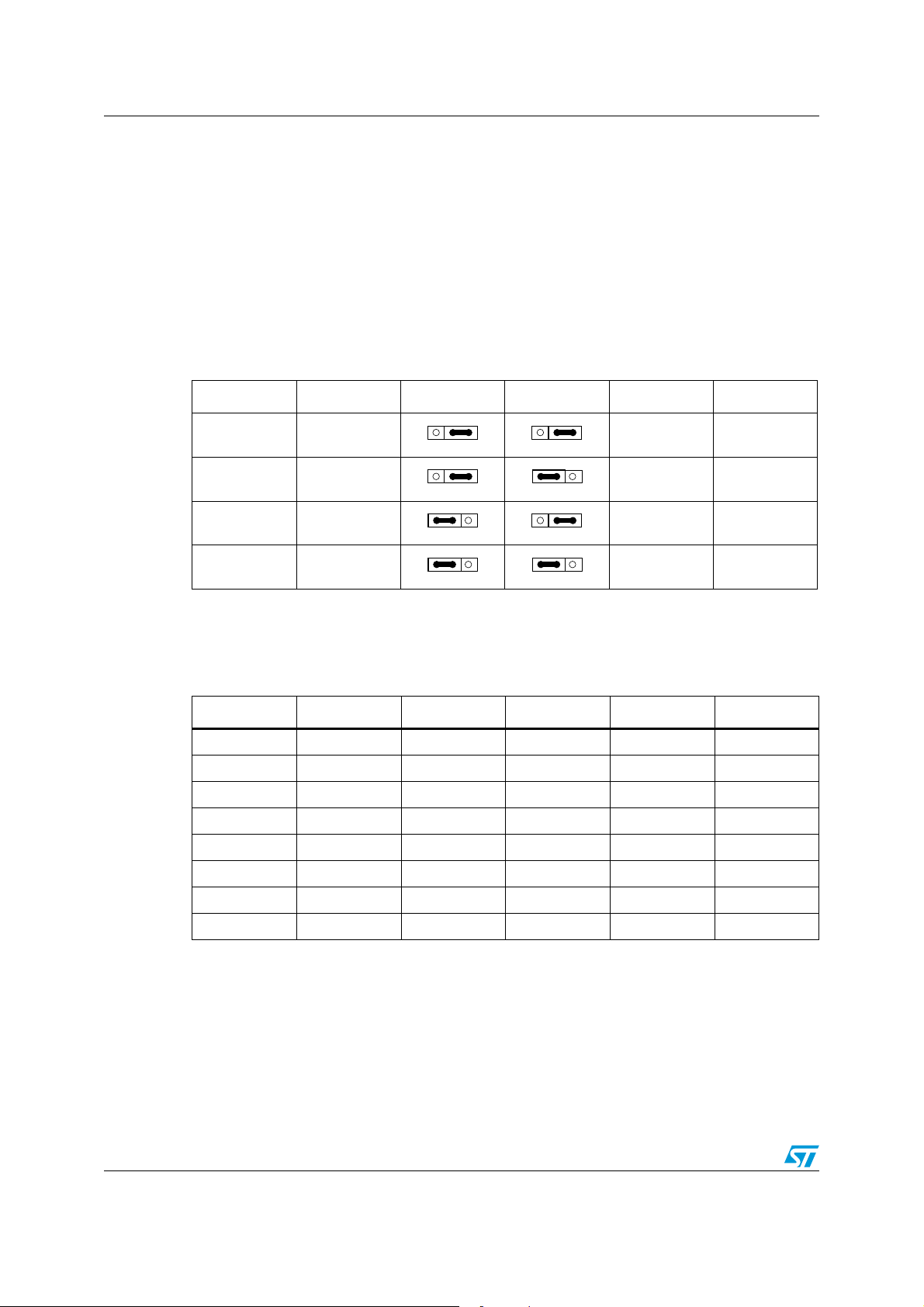
Table 1. Gain settings with G0 and G1 pins
G1 G0 S1 S2 Gain (dB) Gain (V/V)
00 3.51.5
01 62
10 9.53
11 124
`
123
`
123
`
123
`
123
`
123
`
123
`
123
`
123
Note: An internal 300 kΩ (+/-20%) resistor is placed between pins G0, G1 and GND. When the
pins are floating (S1 and S2 included), the gain is 3.5 dB. In full standby (left and right
channels OFF), these resistors are disconnected (HiZ input).
Table 2. Truth table for 3D effect pin and STANDBY pins
3D STBYL STBYR 3D Effect Left channel Right channel
0 0 0 X STDBY STDBY
001OFFSTDBYON
010OFFONSTDBY
011OFFONON
1 0 0 X STDBY STDBY
1 0 1 N/A N/A N/A
1 1 0 N/A N/A N/A
1 1 1 ON ON ON
2/10
Page 3

AN2933 Description of the demonstration board
Note: 1 An internal 300 kΩ (+/-20%) resistor is placed between pins STBYL, STBYR, 3D and GND.
When the 3D pin is floating (S5 included), the 3D effect is switched off. When pins STBYL,
STBYR are floating (S3 and S4 included), the amplifier is in full standby mode. In full
standby (left and right channels OFF), the internal resistors of the gain and 3D effect pins
(G0, G1 and 3D) are disconnected (HiZ input).
2 When the 3D effect is switched on, both channels must be in operation or in shutdown mode
at the same time.
The amplifier’s inputs are capacitor-coupled, meaning that the -3 dB cut-off frequency F
Hz is:
c
with Z
in Ω, Cin in Farads, C1 = C2 and C3 = C4.
in
3 On the TS4999 demonstration board, C
impedance Zin changes with the set gain, as does F
⋅⋅
2π Z
inCin
= C1 = C2 = C3 = C4 = 220 nF. The input
in
.
C
1
-------------------------------------=
F
More information on component calculations is available in the TS4999 datasheet.
c
in
3/10
Page 4

Description of the demonstration board AN2933
Table 3. Demonstration board connectors
Connector(s) Description
P1 Power connector (V
Gain setting connectors: S1 for the G0, S2 for the G1 pin of the TS4999.
The pins are connected as follows:
– 1 to V
CC
– 2 of S1 to the G0 pin
S1, S2
– 2 of S2 to the G1 pin
– 3 to GND
Jumper position:
– logical "1": pins 1 and 2 are shorted
– logical "0": pins 2 and 3 are shorted
Standby control connector: S3 for the left channel, S4 for the right channel.
The pins are connected as follows:
– 1 to V
CC
– 2 of S3 to the STBYL pin of the TS4999
S3, S4
– 2 of S4 to the STBYR pin of the TS4999
– 3 to GND
Jumper position:
`
– pins 1 and 2 are shorted, the channel is operating.
123
`
– pins 2 and 3 are shorted or pin 2 is floating, the channel is in standby
123
mode.
3D effect control connector.
The pins are connected as follows:
S5
– 1 to V
– 2 to 3D pin of the TS4999
CC
– 3 to GND
`
– pins 1 and 2 are shorted, the 3D effect is ON.
123
`
– pins 2 and 3 are shorted, the 3D effect is OFF.
123
JP1
Left channel input signal connector (GND, L
and GND). Power supply voltage from 2.5 to 5.5 V.
CC
`
123
`
123
+, Lin- and GND)
in
JP2
JP3
Right channel input signal connector (GND, R
Left channel output signal connector (GND, L
JP4 Right channel output signal connector (GND, R
-, Rin+and GND)
in
+, Lo- and GND)
o
-, Ro+and GND)
o
Caution: When you apply the power supply through P1, do not invert the polarity since this will
irreversibly damage the U1 amplifier.
4/10
Page 5
AN2933 Description of the demonstration board
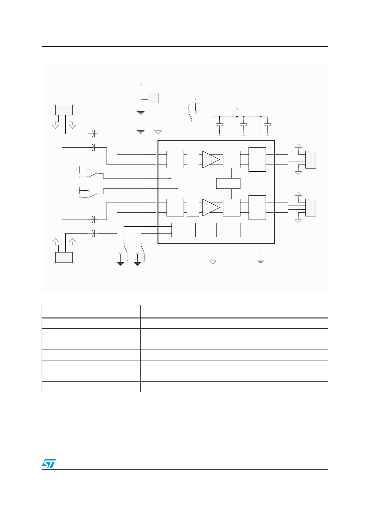
Figure 1. Schematic diagram
Vcc
P1 Vcc
1
Lin+
Lin-
GND
GND
123
4
JP1
C1
220nF
C2
220nF
S1
3
2
1
VCC
G0
S2
3
2
1
VCC
G1
C3
220nF
C4
220nF
123
4
JP2
Rin+
Rin-
GND
GND
LinP
LinN
RinP
RinN
2
S3
STBL
1
3
VCC VCC
2
U1
Lin+
A1
Lin-
B2
G0
C3
G0
C5
G1
G1
E1
Rin+
D2
Rin-
A3
STBYL
STBL
E3
STBYR
STBR
2
TS4999 - FC18
S4
STBR
1
3
Gain
Select
Gain
Select
VCC
Standby
Control
C5
100nF
PWM
Vcc
D6
RPVCC
C6
1uF
LPVCC
H
Bridge
C7
1uF
B6
Lout+
Lout-
A5
A7
JP3
1
2
3
4
Header 4
1
3
S5
3D
2
C13D
D4
AVCC
Oscillator
3D EFFECT
PWM
H
Bridge
Rout+
Rout-
E5
E7
JP4
1
2
3
4
Header 4
Protection
Circuit
PGNDAGND
B4
C7
Table 4. Component list for the demonstration board
Designation Quantity Description
C1, C2, C3, C4 4 220 nF/16 V, SMD ceramic capacitor, 0603
C5 1 100 nF/16 V, SMD ceramic capacitor, 0603
C6, C7 1 1 µF/16 V, SMD ceramic capacitor, 0603
P1 1 2-pin header 2.54 mm pitch
S1, S2, S3, S4, S5 5 3-pin header 2.54 mm pitch
JP1, JP2, JP3, JP4 4 4-pin header 2.54 mm pitch
U1 1 TS4999 class-D audio amplifier
5/10
Page 6

Demonstration board layout AN2933
2 Demonstration board layout
The following figures depict the top view and layers of the demonstration board.
Figure 2. PCB top layer Figure 3. PCB middle layer 1
Figure 4. PCB middle layer 2 Figure 5. PCB bottom layer
6/10
Page 7

AN2933 Demonstration board layout
Figure 6. Top view and dimensions of the demonstration board
7/10
Page 8

Conclusion AN2933
3 Conclusion
To order the board online, go to http://www.st.com/stonline/domains/buy/buy_dev.htm, and
use the order code STEVAL-CCA016V1.
8/10
Page 9

AN2933 Revision history
4 Revision history
Table 5. Document revision history
Date Revision Changes
27-Mar-2009 1 Initial release.
9/10
Page 10

AN2933
Please Read Carefully:
Information in this document is provided solely in connection with ST products. STMicroelectronics NV and its subsidiaries (“ST”) reserve the
right to make changes, corrections, modifications or improvements, to this document, and the products and services described herein at any
time, without notice.
All ST products are sold pursuant to ST’s terms and conditions of sale.
Purchasers are solely responsible for the choice, selection and use of the ST products and services described herein, and ST assumes no
liability whatsoever relating to the choice, selection or use of the ST products and services described herein.
No license, express or implied, by estoppel or otherwise, to any intellectual property rights is granted under this document. If any part of this
document refers to any third party products or services it shall not be deemed a license grant by ST for the use of such third party products
or services, or any intellectual property contained therein or considered as a warranty covering the use in any manner whatsoever of such
third party products or services or any intellectual property contained therein.
UNLESS OTHERWISE SET FORTH IN ST’S TERMS AND CONDITIONS OF SALE ST DISCLAIMS ANY EXPRESS OR IMPLIED
WARRANTY WITH RESPECT TO THE USE AND/OR SALE OF ST PRODUCTS INCLUDING WITHOUT LIMITATION IMPLIED
WARRANTIES OF MERCHANTABILITY, FITNESS FOR A PARTICULAR PURPOSE (AND THEIR EQUIVALENTS UNDER THE LAWS
OF ANY JURISDICTION), OR INFRINGEMENT OF ANY PATENT, COPYRIGHT OR OTHER INTELLECTUAL PROPERTY RIGHT.
UNLESS EXPRESSLY APPROVED IN WRITING BY AN AUTHORIZED ST REPRESENTATIVE, ST PRODUCTS ARE NOT
RECOMMENDED, AUTHORIZED OR WARRANTED FOR USE IN MILITARY, AIR CRAFT, SPACE, LIFE SAVING, OR LIFE SUSTAINING
APPLICATIONS, NOR IN PRODUCTS OR SYSTEMS WHERE FAILURE OR MALFUNCTION MAY RESULT IN PERSONAL INJURY,
DEATH, OR SEVERE PROPERTY OR ENVIRONMENTAL DAMAGE. ST PRODUCTS WHICH ARE NOT SPECIFIED AS "AUTOMOTIVE
GRADE" MAY ONLY BE USED IN AUTOMOTIVE APPLICATIONS AT USER’S OWN RISK.
Resale of ST products with provisions different from the statements and/or technical features set forth in this document shall immediately void
any warranty granted by ST for the ST product or service described herein and shall not create or extend in any manner whatsoever, any
liability of ST.
ST and the ST logo are trademarks or registered trademarks of ST in various countries.
Information in this document supersedes and replaces all information previously supplied.
The ST logo is a registered trademark of STMicroelectronics. All other names are the property of their respective owners.
© 2009 STMicroelectronics - All rights reserved
STMicroelectronics group of companies
Australia - Belgium - Brazil - Canada - China - Czech Republic - Finland - France - Germany - Hong Kong - India - Israel - Italy - Japan -
Malaysia - Malta - Morocco - Singapore - Spain - Sweden - Switzerland - United Kingdom - United States of America
www.st.com
10/10
 Loading...