

Page 1

AN2928
Applica t ion note
Modified buck converter for LED applications
Introduction
The use of high power LEDs in lighting applications is becoming increasingly popular due to
rapid improvements in lighting efficiency, longer life, higher reliability and overall cost
effectiveness. Dimming functions are more easily implemented in LEDs, and they are more
robust and offer wider design flexibility compared to other light sources.
Applications suitable for the use of LEDs include lighting for streets, stadiums, fairs and
exhibitions, shops, interiors, as well as for decorative lighting, outdoor wall lighting and
consumer lighting such as lamps and ballasts. Therefore, LED use for lighting is likely to
represent an increasingly large proportion of the lighting market in the future. To assist
engineers in their design approach, the STEVAL-ILL013V1 80 W offline PFC LED driver
demonstration board has been developed. This application note describes, step-by-step,
all the principles and calculations used for a modified buck converter intended for high
brightness LED applications.
The converter is designed as a constant current source to achieve the best lighting
performance from the LEDs. A “modified buck" topology was chosen because the power
switch is connected to ground rather than the high side switch, as in a standard buck
topology, so with this solution it is easier to control the switch. The design uses a fixed offtime (FOT) network operating in continuous conduction mode (CCM), rendering the overall
solution simple and cost-effective. The modified buck converter described in this document
can be used for lighting applications from low power and low voltage, to high power and high
voltage. This allows designers to cover a wide range of different LED systems using a single
topology.
Additionally, in lighting applications where the input active power is higher than 25 W and
a high power factor is required, the high PF converter can be connecte d as the first stage,
before the modified BUCK converter. The STEVAL-ILL013V1 shows this design concept.
The STEVAL-ILL013V1 demonstration board is an 80 W offline dimmable LED driver with
high power factor (PF) intended for 350 mA, 700 mA and 1 A LEDs, and is based on
STMicroelectronics’ L6562A transition-mode PFC controller. The design is complaint with
standard EN61000-3-2 (limits for harmonic current emissions). The order code is STEVALILL013V1 and the complete design, including schematic diagram, bill of material,
calculations, measurements, etc. is described in user manual UM0670 (see Section 3:
Reference and related materials).
March 2009 Rev 1 1/21
www.st.com
Page 2

Contents AN2928
Contents
1 Modified buck converter in constant current mode . . . . . . . . . . . . . . . . 4
2 Design equations for the modified buck converter . . . . . . . . . . . . . . . . 6
2.1 Basic equations for the modified buck converter . . . . . . . . . . . . . . . . . . . . 6
2.2 Fixed off-time network calculation . . . . . . . . . . . . . . . . . . . . . . . . . . . . . . . 8
2.3 LED current calculation . . . . . . . . . . . . . . . . . . . . . . . . . . . . . . . . . . . . . . 10
2.4 Power MOSFET calculation . . . . . . . . . . . . . . . . . . . . . . . . . . . . . . . . . . . 11
2.5 Power diode selection . . . . . . . . . . . . . . . . . . . . . . . . . . . . . . . . . . . . . . . 14
2.6 Inductor calculation . . . . . . . . . . . . . . . . . . . . . . . . . . . . . . . . . . . . . . . . . 15
3 Reference and related materials . . . . . . . . . . . . . . . . . . . . . . . . . . . . . . 19
4 Revision history . . . . . . . . . . . . . . . . . . . . . . . . . . . . . . . . . . . . . . . . . . . 20
2/21
Page 3

AN2928 List of figures
List of figures
Figure 1. Modified buck converter - tON time. . . . . . . . . . . . . . . . . . . . . . . . . . . . . . . . . . . . . . . . . . . . 4
Figure 2. Modified buck converter - t
Figure 3. Modified buck converter - theory of operation . . . . . . . . . . . . . . . . . . . . . . . . . . . . . . . . . . . 6
Figure 4. Sawtooth signal . . . . . . . . . . . . . . . . . . . . . . . . . . . . . . . . . . . . . . . . . . . . . . . . . . . . . . . . . 12
Figure 5. Real drain MOSFET current. . . . . . . . . . . . . . . . . . . . . . . . . . . . . . . . . . . . . . . . . . . . . . . . 13
Figure 6. Real power diode current . . . . . . . . . . . . . . . . . . . . . . . . . . . . . . . . . . . . . . . . . . . . . . . . . . 15
time . . . . . . . . . . . . . . . . . . . . . . . . . . . . . . . . . . . . . . . . . . . 5
OFF
3/21
Page 4

Modified buck converter in constant curren t mode AN2928
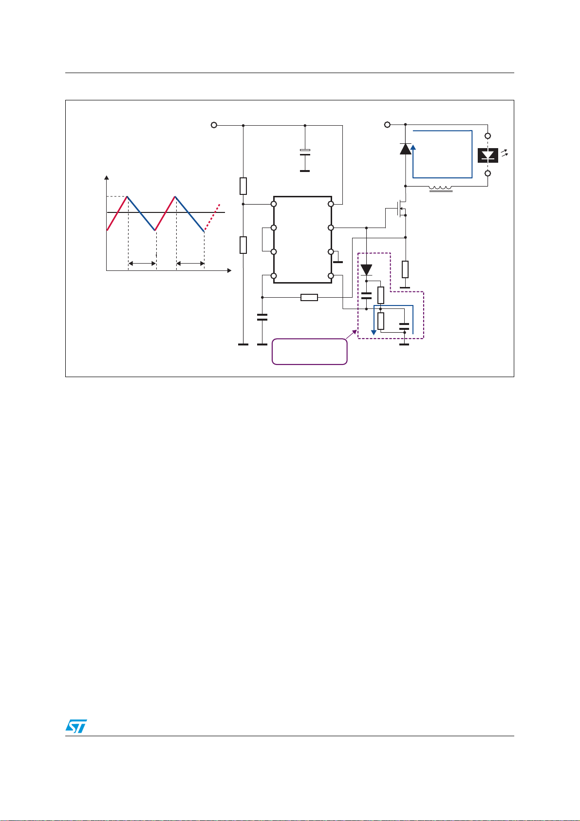
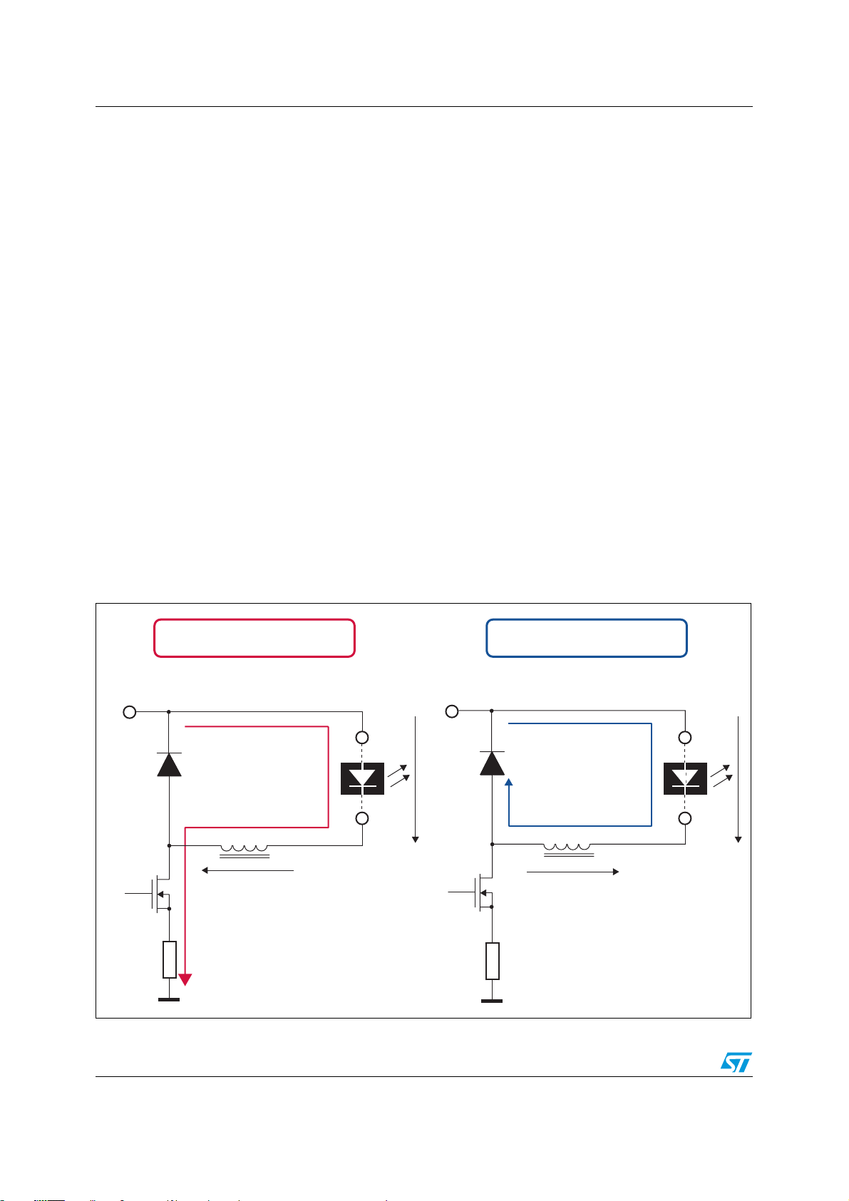
1 Modified buck converter in constant current mode
As stated in the introduction, the aim of this application note is to describe a modified buck
converter working in FOT and CCM. The basic principle of the design using the L6562A
controller is shown in Figure 1 and Figure 2. Figure 1 represents the stage when the power
MOSFET Q
input (V
sensing resistor. Capacitor C
Q
is open and its gate voltage is around 10 V. During the tON time, the load current
1
increases and stops as soon as the voltage on the current sense resistor reaches the
internal threshold on the CS pin of the L6562A. The current sense of the L6562A is clamped
at 1.08 V (typ). Figure 2 shows the t
inductor keeps the current flowing in the same direction and the circuit is closed through
diode D
network (t
R
. The voltage on capacitor C4 is connected to the ZCD (zero current detector) pin of the
4
L6562A. As soon as the capacitor is discharged and its voltage falls below 0.7 V (the ZCD
threshold), the L6562A switches the power MOSFET again and the load current is
increased. This pr ocess repeat s cycle-b y-cycl e, as shown in the ti ming diag rams in Figure 1
and Figure 2.
is turned on. As shown by the red arrow, the current flows from the DC volt age
1
) through the load (LEDs), the inductor (L), the power MOSFET Q1 and the
IN
. The load current is decreasing and the minimum current is set by the fixed off-time
1
time is always constant), because capacitor C4 is discharged to the resistor
OFF
is charged via diode D2 and resistor R5, since the transistor
4
time, when the power MOSFET is switched off. The
OFF
Figure 1. Modified buck converter - t
V
C
I
LED
R
I
_MAX
I
_AVR
I
_MIN
R
FOT
t
t
ON
OFF
-
FOT- fixed off-time
-
t
ON
FOT
t
OFF
t
t
t
1
2
ON
time
C
1
VCC
INV
L6562A
GND
ZCD
R
3
GD
COMP
MULT
CS
C
2
Fixed off-time
network
V
IN
Q
R
LEDs
load
L
1
S
AM00366
D
1
t
ON
D
2
C
R
3
R
5
C
4
4
4/21
Page 5
AN2928 Modified buck converter in constant current mode
Figure 2. Modified buck converter - t
V
C
I
LED
R
I
_MAX
I
_AVR
I
_MIN
FOT
t
t
OFF
-
t
ON
ON
FOT-fixed off-time
FOT
t
OFF
1
R
2
t
OFF
time
C
1
INV
L6562A
COMP
MULT
CS
C
2
Fixed off-time
network
VCC
GND
ZCD
R
3
GD
V
IN
D
t
OFF
1
LEDs
load
L
Q
1
D
2
C
3
R
4
R
S
R
5
C
4
AM00367
5/21
Page 6
Design equations for the modified buck converter AN2928
2 Design equations for the modified buck converter
This section provides all the calculations required for a designer to develop an application
with the modified buck converter working in FOT and CCM. The equations are described
step-by-step, following an application design procedure. First, the basic equations for this
type of converter are shown, then the components for the t
proper power diode and power MOSFET is selected, and finally the power inductor
calculation is demonstrated.
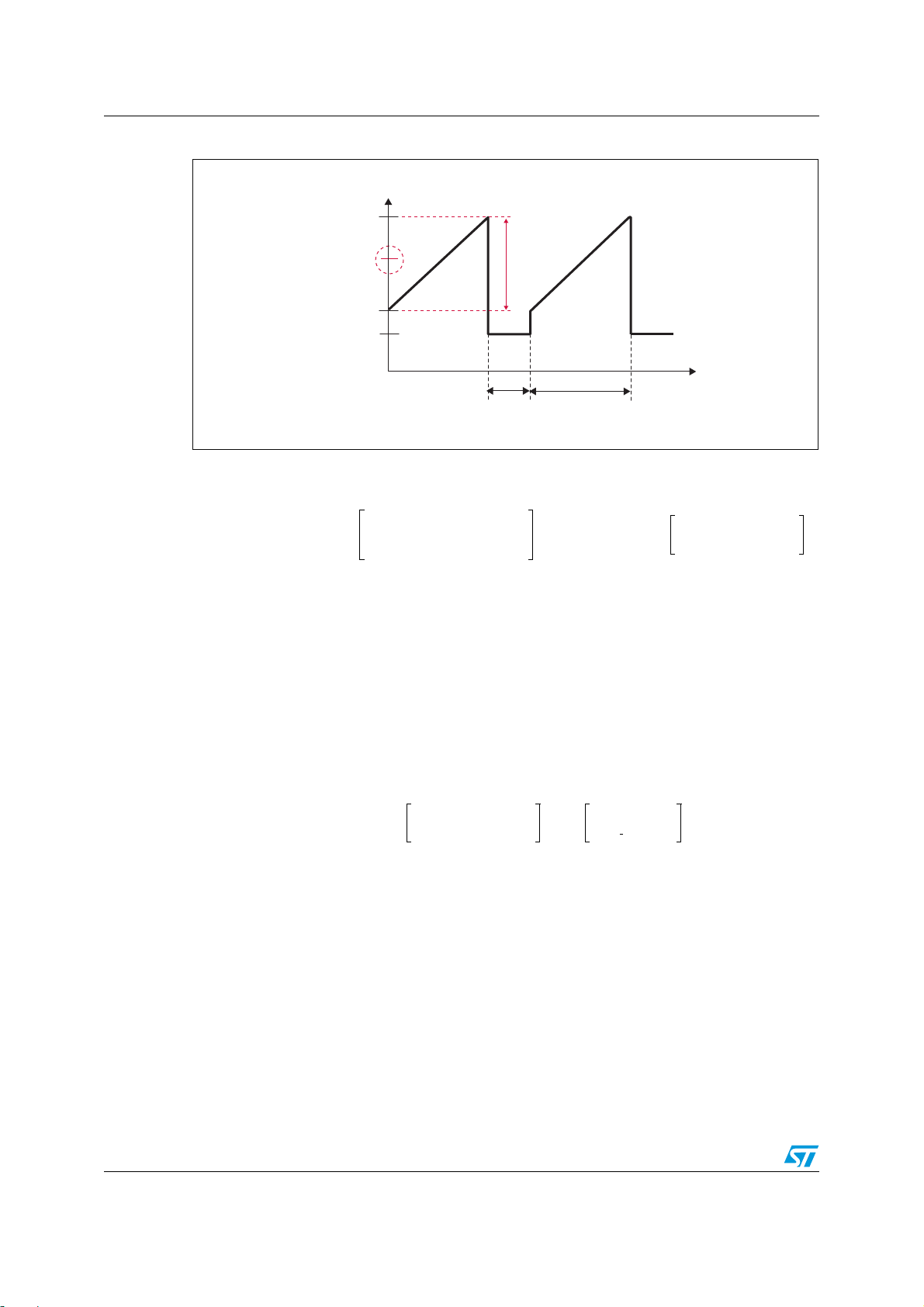
2.1 Basic equations for the modif ied buck conver ter
time are calculated, the
OFF
Figure 3 shows basic circuit stage during tON and t
component references used in the equations.
The voltage across the inductor L is calculated using the following equation:
Equation 1
VLL
= inductor voltage (V)
V
L
L = inductance (H)
= inductor current (A)
I
L
Figure 3. Modified buck convert er - the or y of operation
⋅=
tON time t
V
IN
LEDs
D
1
LEDs
load
V
LED
V
IN
D
1
time, with indicated voltage and
OFF
dI
L
--------
dt
time
OFF
LEDs
load
V
LED
L
t
ON
VL = VIN -V
Q
1
R
S
6/21
-
LED
t
OFF
Q
R
L
VL = V
LED
1
S
AM00368
Page 7

AN2928 Design equations for the modified buck converter
Using Equation 1, it is possible to calculate an inductor current change during tON and t
time:
Equation 2
t
ON
∆I
LON
V
------
∫
L
0
VINV
L
td
–()tON⋅
--------------------------------------------------==
LED
L
Equation 3
tONt
+
OFF
∆I
LOFF
∆I
= inductor current change during tON time (A)
L_ON
∆I
V
V
t
ON
t
OFF
= inductor current change during t
L_OFF
= input voltage (V)
IN
= LED (load) voltage (V)
LED
= turn-on time (s)
= turn-off time (s)
∫
t
ON
OFF
In CCM, the inductor current change during t
V
L
------
L
time (A)
ON
td
and t
V
⋅
LEDtOFF
---------------------------------–==
L
time is the same:
OFF
OFF
Equation 4
∆l
=
LON∆ILOFF
Using Equation 2 and Equation 3, it is possible to create following equations:
Equation 5
VINV
–()tON⋅
--------------------------------------------------
LED
L
V
–()
LEDtOFF
------------------------------------=
L
Equation 6
V
INtONVLEDtONVLEDtOFF
⋅=⋅–⋅
Equation 7
V
INtONVLEDtOFFtON
+()V
LED
T⋅=⋅=⋅
The duty cycle for the modified buck topology (also valid for a standard buck topology)
converter is calculated:
Equation 8
t
V
ON
---------
D
LED
------------- -==
T
V
IN
7/21
Page 8

Design equations for the modified buck converter AN2928
2.2 Fixed off-time network cal culation
The basic idea for this type of converter is to obtain a constant off-time when the power
MOSFET is turned off. This design approach is quite simple and cost-effective, because the
constant off-time is easily set by the RC network. Its calculation is described in this section.
The duty cycle is defined by the switching frequency and turn-off time:
Equation 9
t
---------
D
f = switching frequency in CCM (Hz)
T = period i n CCM (s)
D = duty cycle (-)
From Equation 8 and Equation 9, the turn off-time can be calculated (the switching
frequency is selected):
Equation 10
ON
T
–
Tt
OFF
---------------------
T
1ft
OFF
t
OFF
-----------
1
T
V
LED
------------- -=⋅–
V
IN
⋅–===
1=– ft
OFF
Equation 11
V
LED
⎛⎞
1
------------- -–
⎝⎠
V
IN
OFF
---------------------------- -=
f
t
As stated above, the modified buck converter uses a FOT network. The off-time is set by
resi stor R
the power MOSFET is high, diode D
clamped at V
MOSFET is low, diode D
and capacitor C4, as shown in Figure 2. During the on-time, the gate voltage of
4
ZCD_CLAMP
≈ 5.7 V. During the off-time, the gate voltage of the power
is closed and the voltage at the ZCD pin decreases based on an
2
is opened and the voltage at the ZCD pin is internally
2
exponential law:
Equation 12
1
⎛⎞
---------------- -----
⎝⎠
⋅
R
V
ZCDVZCD CL AMP
4C4
e
⋅=
The voltage at the ZCD pin decreases until it reaches the internal triggeri ng limit, which
causes switching to the turn-on stage. The trigger voltage for the L6562A is 0.7 V. The time
needed for the ZCD voltage to go from V
the off-time t
OFF
:
ZCD_CLAMP
to V
ZCD_TRIGGER
defines the duration of
Equation 13
V
⎛⎞
t
OFF
R4C
ZCD CL AMP
---------------------------------------- -
⎜⎟
4
V
⎝⎠
ZCD TRIGGER
R
4C4
5.7
⎛⎞
--------
ln R
⎝⎠
0.7
4C4
2.1⋅⋅=⋅⋅=ln⋅⋅=
8/21
Page 9

AN2928 Design equations for the modified buck converter
V
= voltage on the ZCD pin of the L6562A (V)
ZCD
V
ZCD_CLAMP
V
ZCD_TRIGGER =
Capacitor C
= clamp voltage on the ZCD pin of the L6562A (V)
trigger voltage on the ZCD pin of the L6562A (V)
can be selected, and the resistor is easily calculated using Equation 14, or the
4
inverse can be calculated with Equat ion 15 .
Equation 14
t
OFF
----------------------=
R
4
2.1 C4⋅
Equation 15
t
C
OFF
----------------------=
4
2.1 R4⋅
Resistor R
C
during the tON time, and must be within the following range (as described in application
4
(shown in Figure 2) is designed to limit the charge current flowing to capacitor
5
note AN1792. See Section 3: Reference and related materials).
Equation 16
V
GD MAXVZCD CLAMP
-------------------------------------------------------------------------------
l
V
= diode D2 forward voltage (V) (typically 0.7 V)
F
V
ZCD_CLAMP
V
GD_MAX
V
GD_MIN
I
ZCD_MAX
If the t
= clamp voltage on the ZCD pin of L6562A (V) (5.7 V)
= output high - maximum gate driver voltage (V) (15 V)
= output high - minimum gate driver voltage (V) (9.8 V)
= maximum sink capability for the ZCD pin (A) (0.01 A)
time is very short (light load or low output voltage), then capacitor C4 cannot be
ON
quickly charged via resistor R
parallel with resistor R
– VF–
ZCD MAX
⎛⎞
V
GD MINVZCD CLAMP
⎜⎟
5R4
⋅<<
----------------------------------------------------------------------------- -
⎜⎟
⎝⎠
V
ZCD CLAMP
---------------------------------- -+
R
4
. Therefore it is recommended to connect capacitor C3 in
5
. The maximum size of capacitor C3 can be calculated with the
5
R
– VF–
V
ZCD CL AMP
following equation:
Equation 17
C3C
<
V
------------------------------------------------------------------------------------
4
V
GD M AXVZCD CLAMP
ZCD CL AMP
– VF–()
9/21
Page 10

Design equations for the modified buck converter AN2928
2.3 LED current calculation
The preceding equations (Equation 12 through 17) are used to calculate the FOT network
using resistors R
circuit because the output LED current and inductor must be calculated. For the inductor
current change, the following equation is used:
Equation 18
and R5 and capacitors C3 and C4. At this point, focus shifts to the power
4
∆lLl
∆I
= inductor (LED) current change (A)
L
= maximum (LED) inductor current (A)
I
MAX
= minimum (LED) inductor current (A)
I
MIN
= average (LED) inductor current (A)
I
AVR
MAXlMIN
2l
MAXlAVR
–()⋅=–=
Combining Equat ion 18 and Equation 3, considering the current change as an absolute
value (i.e. positive), it is possible to derive:
Equation 19
V
⋅
LEDtOFF
where t
--------------------------------- 2l
∆l
L
is calculated using Equation 11.
OFF
L
–()⋅==
MAXlAVR
From Equation 11 and Equation 19 the equation for deriving the inductor size can be
formulated (maximum and average LED current is selected):
Equation 20
V
L
------------------------------------------------------
2l
1D–()⋅
LED
–()f⋅⋅
MAXlAVR
⋅
V
LEDtOFF
---------------------------------------------==
2l
–()⋅
MAXlAVR
Sense resist or R
can be easily calculated because the voltage threshold on the CS pin for
S
the L6562A is 1.08 V and therefore the resistor size is fol lowing:
Equation 21
R
S
V
= current sense threshold (V)
CS
Although the modified buck converter using the FOT network and working in CCM that is
described here works as a constant current source, a limitation is the current dependency
on the output voltage (number of LEDs). To understand this limitation it is necessary to
derive the average inductor current (which is the LED current) from Equation 20. The result
is shown in Equation 22, which provides the information listed.
10/21
V
CS
------------
l
MAX
1.08
----------- -==
l
MAX
Page 11

AN2928 Design equations for the modified buck converter
Equation 22
V
l
AVRlMAX
●
I
is constant and set by the resistor R
MAX
t
●
●
●
is constant and set by the FOT network
OFF
The average inductor (LED) current is independent of the input voltage
The average inductor (LED) current depends slightly on the voltage across the LEDs
--------------------------------------- l
LED
2Lf⋅⋅
1D–()⋅
S
MAX
V
⋅
LEDtOFF
---------------------------------–=–=
2L⋅
(i.e. number of LEDs) and therefore the design shows the best results using a fixed
number of LEDs. A variable number of LEDs results in less current precision.
2.4 Power MOSFET calculation
The power MOSFET is chosen based on maximum stress voltage, maximum peak
MOSFET current, total power losses, maximum allowed operating temperature and the
driver capability of the L6562A.
Maximum stress voltage on the power MOSFET (drain-source voltage) for this modified
buck converter is equal to the input voltage. The power MOSFET must be selected with
some voltage margin. For example, if the input voltage is maximally 400 V, then maximum
drain-source voltage should be 450 V or higher.
Maximum peak MOSFET current was selected in order to calculate the inductor size in
Equation 20. Also in this case, the power MOSFET must be chosen with some current
margin.
Total power losses on the power MOSFET must be calculated, due to the importance of
designing a proper heat sink to avoid temperature stress on the power MOSFET. Basically,
total power losses on the power MOSFET occur through conduction losses (depending on
the R
), switching losses and gate charge loss caused by charging up the gate
DS(ON)
capacitance and then discharging this capacitance to ground. The gate charge loss is very
small compared to the conduction and switching losses, so it is not used for further
calculations. For total power MOSFET loss, a valid equation is:
Equation 23
P
P
= total power losses on the power MOSFET (W)
TOT
= conduction losses on the power MOSFET (W)
P
CON
= switching losses on the power MOSFET (W)
P
SW
TOT
P
+=
CONPSW
The power MOSFET conduction loss is represented by the continuous conduction current
flowing through the MOSFET during the on-time stage. Therefore, the power loss depends
on its static drain- so ur ce resist ance (R
). In order to calculate conduction loss
DS(ON)
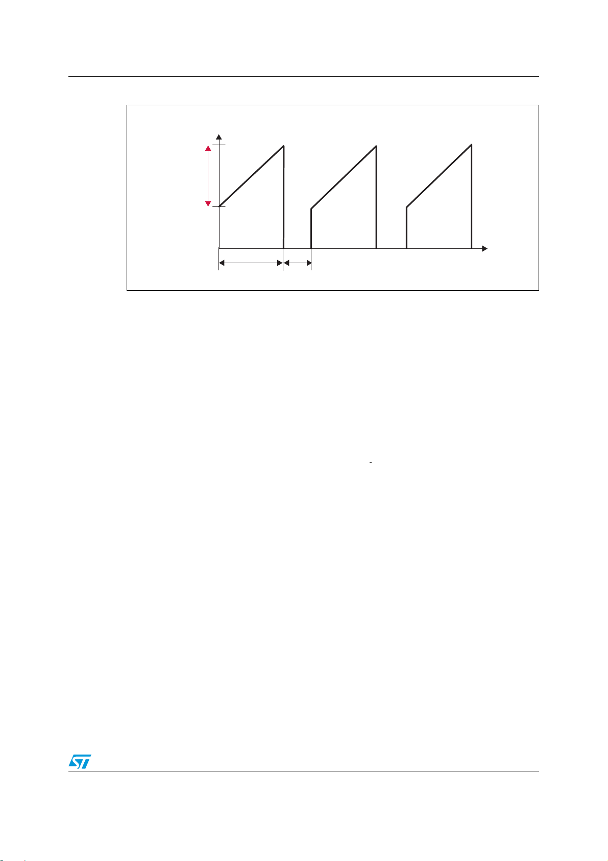
properly, it is necessar y to calculate the drain current RMS value. Figure 4 shows the
sawtooth signal for which the RMS value was calculated in Equation 24. Note that in this
case, average current I
((I
MAX+IMIN
)/2).
is defined as the average value of the sawtooth portion
AVR
11/21
Page 12
Design equations for the modified buck converter AN2928
Figure 4. Sawtooth signal
i(t)
l
MAX
t
ON
I
PP
t
OFF
l
AVG
l
MIN
I
0
t
DT (1- D)T
t
0
-
AM00369
Equation 24
t0T+
1
2
l
=
RMS
I
= root-mean squared drain current (A)
RMS
= peak-to-peak current (A) (difference between I
I
PP
2
-- -
T
t() t
i
∫
t
0
t0DT+
1
---
T
i2t() ti
∫
t
0
T+
t
0
2
+d
t0DT+
t() t··d
∫
D= l
_MAX
2
0
and I
1D–()⋅+⋅
_MIN
l
+
MAXlMIN
⎛⎞
-----------------------------
⎝⎠
2
)
2
2
l
PP
------- -+=d
12
The real drain current waveform is given in Figure 5. As can be observed, the signal is quite
similar to the signal in Figure 4, except that there is no current during the off-time stage
= 0) and the on and off-times are reversed. Therefore, for real current Equation 24 is
(I
O
modified to become Equation 25.
Square RMS drain current is calculated using the equation:
Equation 25
l
+
MAXlMIN
⎛⎞
-----------------------------
⎝⎠
2
I
AVR_ON
2
l
RMS
D
= average current during tON time (A) (see Figure 5).
And finally it is possible to calculate the continuous conduction losses:
Equation 26
P
CONlRMS
R
12/21
= static drain-source on resistance for working MOSFET temperature (Ω).
DS(ON)
2
2
l
PP
------- -+ D= l
12
2
⋅=
R
DS ON()
2
AVR ON
l
------- -+⋅⋅=
12
2
PP
Page 13
AN2928 Design equations for the modified buck converter
Figure 5. Real drain MOSFET current
i
i(t)
I
MAX
I
PP
I
MIN
t
t
ON
t
OFF
AM00371
The second part of the MOSFET losses is switching losses, which depend on the (on and
off) switching time, drain MOSFET current, drain-source voltage and the switching
frequency . The s witching time, rise time and fall time is a function of the gate-to-drain “Miller”
charge of the MOSFE T (Q
(V
), and the minimum gate voltage which enables the current through the drain source
GS(TH)
), the internal resistance of the driver, the threshold voltage
_GD
of the MOSFET. As the correct calculation of switching power losses is complex due to non
linear behavior of the switch, it is not possible to obtain an exact equation for the calculation
of switching losses. Moreover, the s witching behavior is also influenced by the performance
of the driver and layout design (leakage inductance and parasitic capacitors). To arrive at an
estimation of the switching power losses, Equation 27 can be used.
Equation 27
t
OFF_SW
VINl
------------------------------------------------------------------- -=
MAXtOFF SW
P
SW
= switch off-time (s) (typically tens of ns).
2
f⋅⋅ ⋅
For example, switched off-time measured on the STEVAL-ILL013V1 using the STP9NM50N
power MOSFET (400 V input voltage) is 120 ns.
Total power (P
) is lost in the power MOSFET and its heat sink, so it is simple to
_TOT
calculate:
Equation 28
T
–
P
TOT
T
= maximum junction temperature (°C)
JMAX
= ambient temperature (°C)
T
A
= junction-to-case thermal resistance (°C/W)
R
thJC
= case-to-heat sink thermal resistance (°C/W) (usually between 0.35 and 0.8 for the
R
thCH
JMAXTA
------------------------------------------------------------=
R
++
thJCRthCHRthHA
insulating washer)
= heat sink-to-ambient thermal resistance (°C/W)
R
thHA
13/21
Page 14

Design equations for the modified buck converter AN2928
Finally, if the heat sink and its thermal resistance is known, it is possible to calculate
maximum static drain-source on resistance from Equation 26, Equation 27 and Equation 28
for easy power MOSFET selection.
Equation 29
R
DS ON()
------------------------------------------------------------------------------------ -
R
++()l
thJCRthCHRthHA
2.5 Power diode selection
The power diode (D1 from Figure 1) is chosen based on its maximum stress voltage, its
maximum peak current and total power losses. The power losses are lower for a larger duty
cycle and vice-versa, because the diode is opened (connected) during off-time.
Maximum voltage stress across the diode is equal to the input voltage V
power diode must be selected with some voltage ma rgin. For example, if the input voltage is
maximally 400 V, then maximum repetitive peak reverse voltage (V
higher.
Maximum peak diode current is selected in order to calculate the inductor size in
Equation 20. Also in this case, the power diode must be selected with some current margin.
Power losses are generally calculated with the following equation:
Equation 30
T
JMAXTA
P
LOSS D
–
⋅
T
1
---
i
=
D
∫
T
0
V
INlMAXtOFF SW
------------------------------------------------------------------- -–<
2
RMS
t() uD⋅ t()td
2
⋅
2l
RMS
RRM
f⋅⋅ ⋅
and therefore the
IN,
) should be 450 V or
P
LOSS_D
= power diode current (A)
i
D
u
D
= power diode losses (W)
= power diode voltage (V)
And assuming a constant voltage drop over the diode it is possible to approximately
calculate the power losses on the diode (switching losses are not included) with the
following equation:
Equation 31
P
LOSS DIAVR DVF
= power diode average current (A)
I
AVR_D
= power diode forward voltage for calculated average diode current (V)
V
F
14/21
⋅=
Page 15

AN2928 Design equations for the modified buck converter
where the average diode current is shown in Figure 6 and can be calculated using:
Equation 32
+
I
MAXIMIN
⎛⎞
I
AVR D
ID–()
------------------------------
⋅=
⎝⎠
2
And finally the junction diode temperature without using the heat sink can be calculated from
the following equation (ambient temperature is chosen):
Equation 33
TJP
T
= power diode junction temperature (°C)
J
= case-to-ambient thermal resistance (°C/W) (for example, the T O-220 package has a
R
thCA
LOSS D
R
+()TA+⋅=
thJCRthCA
typical thermal resistance of 60 °C/W)
The calculated power diode junction temperature must be lower then maximum diode
junction temperature T
. For proper design, it is recommended to keep the junction
JMAX
temperature much lower than its maximum in order to avoid temperature stress on the
power diode.
Equation 34
Figure 6. Real power diode current
i
i(t)
I
MAX
I
PP
I
MIN
t
ON
2.6 Inductor calculation
t
OFF
TJT
<
JMAX
t
AM00370
All components for the design are calculated, but the final step in the design procedure still
remains, since it is necessary to calculate the inductor (L). The calculations that follow are
valid for the inductor used in the STEVAL-ILL013V1 demonstration board, but for
applications with (for example) lower voltages, some standardized inductors for DC-DC can
als o be used.
15/21
Page 16

Design equations for the modified buck converter AN2928
First, the inductor core size must be selected, for which it may be helpful to calculate the
minimum area product using application parameters. The minimum required core area
product (AP), where the flux swing is limited by core saturation is:
Equation 35
4
-- -
LI
⋅⋅
PEAKIRMS
⎛⎞
AP
AP
= minimum area product (cm4)
MIN
= inductor peak current (A)
I
PEAK
= inductor RMS current (A)
I
RMS
= saturation limited flux density (T) (pow er ferrites like N27 or N67 have typically 0.3 T)
B
MAX
----------------------------------------------
=
MIN
⎝⎠
B
MAX
3
Cl⋅
Equation 36
Cl J
J
= maximum current density (A/cm2) (That commonly used for natural convection
MAX
cooling is 420 A/cm
= ratio of the total copper area to the window area (-)
C
R
The constant C
2
)
gives an estimation of how effectively the wires are placed on the core. For
R
⋅⋅=
MAXCR
10
4–
example, if the input vol tage of the modified buc k converter is 400 V (such as when a power
factor preregulator is used), then the wires must be well-isolated and the ratio between the
copper and window area is about 0.5, which in the end means that there is 50% of the wire
on the inductor core. The exact calculation using the equation listed here can be found in the
user manual UM0670 (see Section 3: Reference and related materials).
Once the minimum area product is calculated, the designer should then select the right
inductor core and ferrite material according to the higher AP value. The AP value is
calculated from the winding cross section and core cross section. For example, the ETD29
core with ferrite material N27 from EPCOS has a winding cross section of 97 mm
a core cross section of 71 mm
2
. Maximum flux density for the N27 is 0.3 T.
2
and
Equation 37
AP A
A
= winding cross section (mm2)
N
= minimum core cross section (mm2)
A
MIN
For a proper inductor core, the calculated area product must be higher than the AP
⋅=
NAMIN
MIN
calculated in Equation 35. If the condition derived from E quation 38 is no t f ulfi lle d, the
designer must select a bigger inductor core.
Equation 38
AP
MIN
AP<
A simple way how to calculate the number of inductor turns is shown in Equation 39, since
manufacturers also include the inductance factor A
which depends on air gap, in the
L,
product datasheets. For example, the ETD29 core with 1 mm gap and N27 ferrite material
has an inductance factor of 124 nH.
16/21
Page 17

AN2928 Design equations for the modified buck converter
Equation 39
LN2AL⋅=
= inductance factor (H)
A
L
N = inductor numb er of t urns (-)
The number of turns for the inductor is:
Equation 40
L
------=
N
A
L
After the number of turns is calculated, it is also necessary to calculate the wire diameter.
The maximum power loss can be calculated using the maximum inductor temperature and
core thermal resistance with the following equation:
Equation 41
T
–
P
MAX LOSS
MAXTA
---------------------------=
R
T
P
MAX_LOSS
T
MAX
= thermal resistance of the inductor core used (°C/W) (for example, thermal resistance
R
T
= maximum power loss in the inductor (W)
= maximum inductor temperature (°C)
for the E25 core used in the STEVAL-ILL013V1 design is 40 °C/W).
The loss in the core is:
Equation 42
P
COREPV
P
= loss in the inductor core (W)
CORE
= core loss defined in the datasheet (mW/g )
P
V
W10
⋅⋅=
3–
W = core weight (g) (for example, the ETD29 has a weight of 28 g)
Maximum powe r los s in the wire is simply:
Equation 43
= maximum power loss in the wire (W)
P
WIRE
P
WIRE
P
MAX LOSSPCORE
–=
The maximum wire resistance derives from the following equation:
Equation 44
P
R
MAX WIRE
-----------------=
I
WIRE
2
RMS
R
MAX_WIRE
= maximum wire resistance (Ω)
17/21
Page 18

Design equations for the modified buck converter AN2928
Winding resistance depends on the diameter, and is defined using the following formula:
Equation 45
I
Rp
l
--- -
p
S
⋅=⋅=
N
----------------
π d⋅
N⋅
R = wire resistance (Ω)
p = resistivity of the copper (Ω
S = conductor cross-section area (cm
•
cm) (1,76 • 10-6 for temperature 25 °C)
2
)
l = wire length (cm)
= average length of turn (cm)
l
N
d = wire diameter (cm)
The wire diameter is properly selected if the total wire resistance is lower than the maximum
wire resistance.
Equation 46
<
RR
MAX WIRE
18/21
Page 19

AN2928 Reference and related materials
3 Reference and related materials
1. STEVAL-ILL013V1, 80 W offline PFC and LED driver demonstration board with
dimming based on the L6562A; data brief
2. AN1792, Design of fixed-off-time-controlled PFC pre-regulators with the L6562;
application note
3. L6562A, Transition-mode PFC controller; datashe et
4. AN1059, Design equations of high-power-factor Flyback converters based on the
L6561; application note
5. UM0670, 80 W off-line LED driver with PFC; user manual
Note: The reference and related materials listed above are available on the STMicroelectronics
web site at www.st.com.
19/21
Page 20

Revision history AN2928
4 Revision history
Table 1. Document revision history
Date Revision Changes
24-Mar-2009 1 I nitial releas e.
20/21
Page 21

AN2928
y
y
Please Read Caref u ll y:
Information in this document is provided solely in connection with ST products. STMicroelectronics NV and its subsidiaries (“ST”) reserve the
right to make changes, corrections, modifications or improvements, to this document, and the products and services described herein at an
time, with out notice.
All ST products are sold pursuant to ST’s terms and conditions of sale.
Purchase rs are solely responsible for the ch oi ce, selec tion and use of the ST products and services d escribed herein, and ST assumes no
liability whatsoever relating to the choice, selection or use of the ST products and services described herein.
No license, express or implied, by estoppel or otherwise, to any intellectual property rights is granted under this document. If any part of this
document refers to any third party product s or servic es it shall n ot be deeme d a license grant by ST for the use of such third party products
or services , or any intel lec tual pro per ty cont aine d ther ein or consi dere d as a warra nty c overi ng th e use in any mann er w hats oever of such
third party products or services or any intellec tu al property c ont ai ned therein.
UNLESS OTHERWISE SET FORTH IN ST’S TERMS AND CONDITIONS OF SALE ST DISCLAIMS ANY EXPRESS OR IMPLIED
WARRANTY WITH RESPECT TO THE USE AND/OR SALE OF ST PRODUCTS INCLUDING WITHOUT LIMITATION IMPLIED
WARRANTIES OF MERCHANTABILITY, FITNESS FOR A PARTICULAR PURPOSE (AND THEIR EQUIVALENTS UNDER THE LAWS
OF ANY JURISDICTION), OR INFRINGEMENT OF ANY PATENT, COPYRIGHT OR OTHER INTELLECTUAL PROPERTY RIGHT.
UNLESS EXPRESSLY APPROVED IN WRITING BY AN AUTHORIZED ST REPRESENTATIVE, ST PRODUCTS ARE NOT
RECOMM ENDED , AUTHO RIZED OR WARRANT ED FOR USE IN M ILITA RY, AIR CR AFT, SPA CE, LIF E SAVIN G, OR LIF E SUSTAI NING
APPLICATIONS, NOR IN PRODUCTS OR SYSTEMS WHERE FAILURE OR MALFUNCTION MAY RESULT IN PERSONAL INJURY,
DEATH, OR SEVERE PROPERTY O R ENVI RONMEN T AL DAMA G E. S T PR ODUC TS W HIC H ARE NOT SPECIFIED AS "AU TO MOTI VE
GRADE" MAY ONLY BE USED IN AUTOMOTIVE APPLICATIONS AT USER’S OWN RISK.
Resale of ST products with provisions different from the statements and/or technical features set forth in this document shall immediately void
any warran ty gr anted by ST fo r the ST produc t or se rvice d es cribed he rein and shall not c reat e or ex tend in a ny mann er wha tsoe ver, an
liability of ST.
ST and the ST logo are trademarks or regis tered trade m arks of ST in vari ous countri es.
Information in this do cument super sedes and replaces all information pr eviously supplied.
The ST logo is a registered trademark of STMicroelectronics. All other names are the property of their respective owners.
© 2009 STM icroelectronics - All ri ght s reserved
STMicroelectron ics group of com panies
Austra l i a - Belgium - Brazil - Cana da - China - Czech Republic - F i nl and - Franc e - Germany - Ho ng K o ng - India - Isr ael - Italy - Japan -
Malaysi a - M al ta - Morocco - Singapore - Spain - Swe den - Switzerland - Uni ted Kingdom - Uni ted States of America
www.st.com
21/21
 Loading...