

AN2798
Application note
Complete DDR2/3 memory power supply
controller based on the PM6670AS
Introduction
The PM6670AS device is a complete DDR2/3 power supply regulator for portable
applications designed to meet JEDEC specifications . It int egr a tes a constant on-time ( COT)
buck controller, a 2 A peak sink/source low dropout regulator and a 15 mA low-noise
buffer ed reference.
The COT architecture assures fast transient response supporting both polymeric and
ceramic output capacitors. An embedded integrator control loop compensates the DC
voltage error due to the output ripple. The 2 A peak sink/source linear regulator pro vides the
memory termination voltage with fast load transient response.
The device is fully compliant with syst em sleep stat es S3 and S4/ S5, setting the LDO output
to high impedance in suspend-to-RAM state and performing the tracking discharge of all
outputs in suspend-to-disk state.
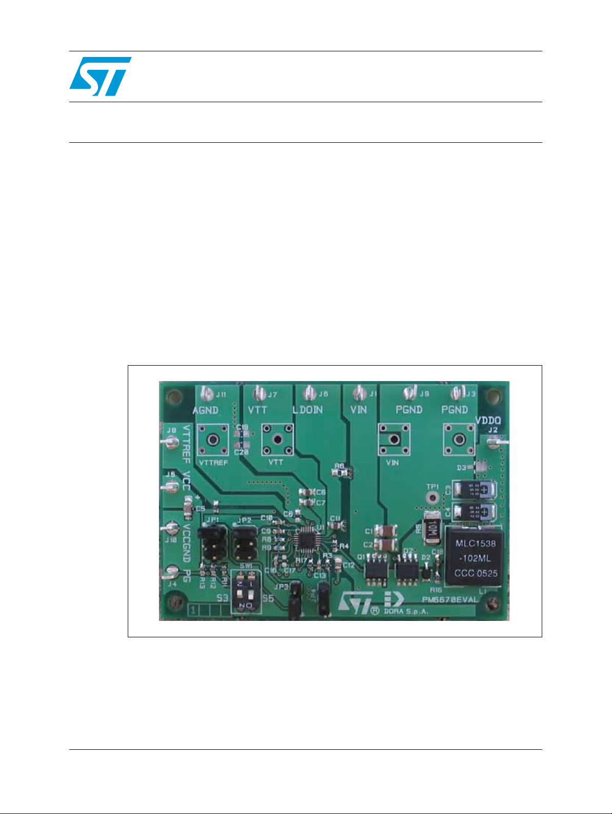
Figure 1. PM6670AS demonstration board
November 2008 Rev 1 1/38
www.st.com
38

Contents AN2798
Contents
1 Main features . . . . . . . . . . . . . . . . . . . . . . . . . . . . . . . . . . . . . . . . . . . . . . . 5
1.1 Switching section (VDDQ) . . . . . . . . . . . . . . . . . . . . . . . . . . . . . . . . . . . . . 5
1.2 Reference and termination voltages (VTTREF and VTT) . . . . . . . . . . . . . 5
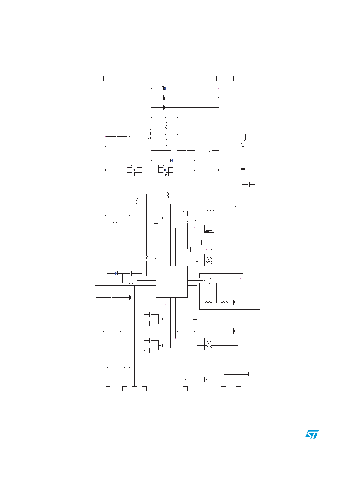
2 Demonstration kit schematic . . . . . . . . . . . . . . . . . . . . . . . . . . . . . . . . . . 6
2.1 Component list . . . . . . . . . . . . . . . . . . . . . . . . . . . . . . . . . . . . . . . . . . . . . . 7
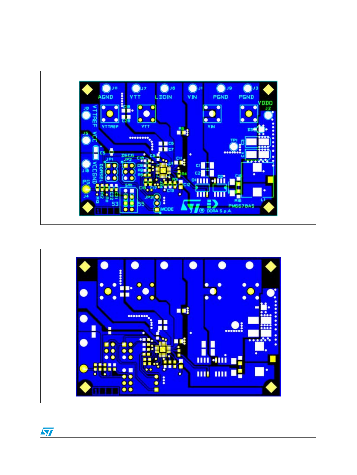
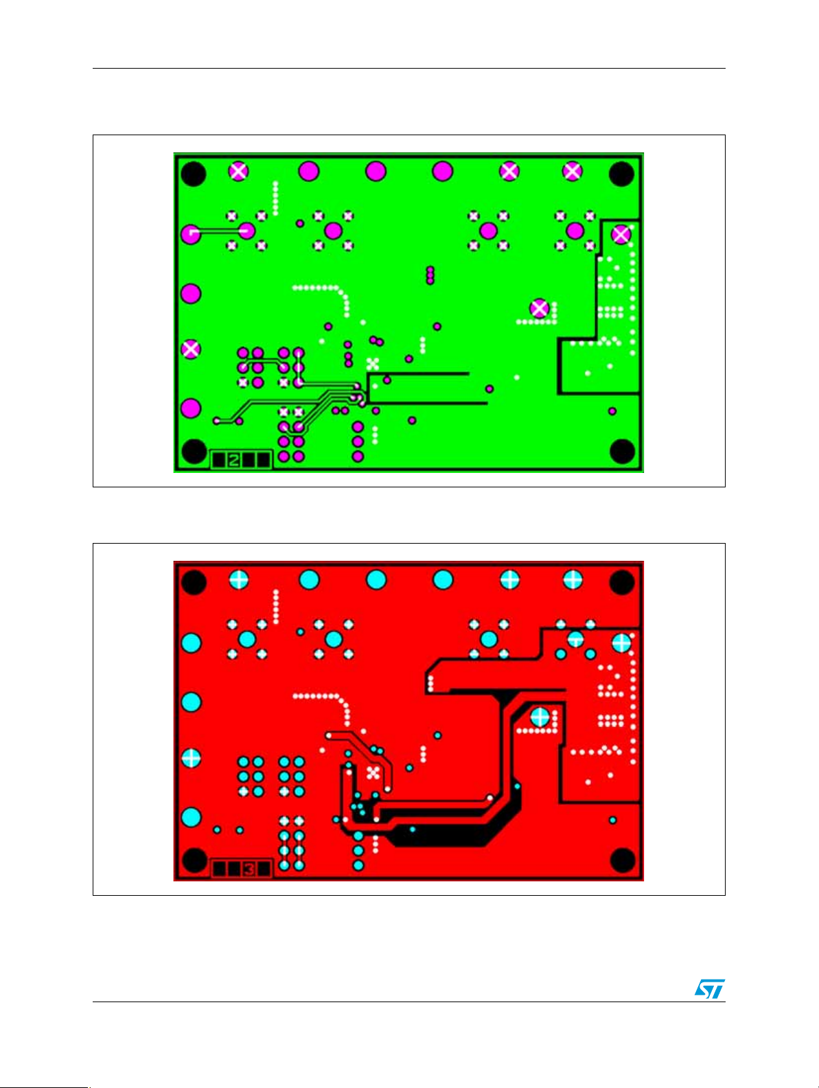
3 Component assembly and layout . . . . . . . . . . . . . . . . . . . . . . . . . . . . . . 9
4 I/O interface . . . . . . . . . . . . . . . . . . . . . . . . . . . . . . . . . . . . . . . . . . . . . . . 12
4.1 Recommended equipment . . . . . . . . . . . . . . . . . . . . . . . . . . . . . . . . . . . . 12
5 Configuration . . . . . . . . . . . . . . . . . . . . . . . . . . . . . . . . . . . . . . . . . . . . . . 13
5.1 JP3 fixed or adjustable output voltage (MODE pin) . . . . . . . . . . . . . . . . . 13
5.2 JP1 DDR2/DDR3 or power-saving mode (DDRSEL pin) . . . . . . . . . . . . . 13
5.3 JP2 output discharge (DSCG pin) . . . . . . . . . . . . . . . . . . . . . . . . . . . . . . 14
5.4 JP5 compensation network (COMP pin) . . . . . . . . . . . . . . . . . . . . . . . . . 15
6 Test setup . . . . . . . . . . . . . . . . . . . . . . . . . . . . . . . . . . . . . . . . . . . . . . . . . 16
7 Getting started . . . . . . . . . . . . . . . . . . . . . . . . . . . . . . . . . . . . . . . . . . . . . 17
7.1 Power-up sequence . . . . . . . . . . . . . . . . . . . . . . . . . . . . . . . . . . . . . . . . . 17
7.2 Power-down sequence . . . . . . . . . . . . . . . . . . . . . . . . . . . . . . . . . . . . . . . 17
8 PM6670AS evaluation tests . . . . . . . . . . . . . . . . . . . . . . . . . . . . . . . . . . 18
8.1 VDDQ, VTT and VTTREF turn-on (soft-start) . . . . . . . . . . . . . . . . . . . . . 18
8.2 VDDQ working modes . . . . . . . . . . . . . . . . . . . . . . . . . . . . . . . . . . . . . . . 19
8.2.1 VDDQ forced PWM mode . . . . . . . . . . . . . . . . . . . . . . . . . . . . . . . . . . . 19
8.2.2 VDDQ pulse-skip mode . . . . . . . . . . . . . . . . . . . . . . . . . . . . . . . . . . . . . 19
8.2.3 VDDQ non-audible pulse-skip mode . . . . . . . . . . . . . . . . . . . . . . . . . . . 20
2/38
8.3 VDDQ, VTT and VTTREF load regulation . . . . . . . . . . . . . . . . . . . . . . . . 20
8.4 VDDQ and VTT load transient responses . . . . . . . . . . . . . . . . . . . . . . . . 22
8.5 VDDQ efficiency . . . . . . . . . . . . . . . . . . . . . . . . . . . . . . . . . . . . . . . . . . . . 23
8.6 VDDQ gate drivers . . . . . . . . . . . . . . . . . . . . . . . . . . . . . . . . . . . . . . . . . . 23

AN2798 Contents
8.7 VDDQ, VTT and VTTREF turnoff (soft-end) . . . . . . . . . . . . . . . . . . . . . . 24
8.8 UV, OV and thermal protections . . . . . . . . . . . . . . . . . . . . . . . . . . . . . . . . 26
8.9 VDDQ current limit . . . . . . . . . . . . . . . . . . . . . . . . . . . . . . . . . . . . . . . . . . 28
8.10 VTT current limit (foldback) . . . . . . . . . . . . . . . . . . . . . . . . . . . . . . . . . . . 30
8.11 Switching frequency . . . . . . . . . . . . . . . . . . . . . . . . . . . . . . . . . . . . . . . . . 31
8.12 Thermal behavior . . . . . . . . . . . . . . . . . . . . . . . . . . . . . . . . . . . . . . . . . . . 33
9 Revision history . . . . . . . . . . . . . . . . . . . . . . . . . . . . . . . . . . . . . . . . . . . 37
3/38

List of figures AN2798
List of figures
Figure 1. PM6670AS demonstration board . . . . . . . . . . . . . . . . . . . . . . . . . . . . . . . . . . . . . . . . . . . . . 1
Figure 2. PM6670AS demonstration board schematic . . . . . . . . . . . . . . . . . . . . . . . . . . . . . . . . . . . . 6
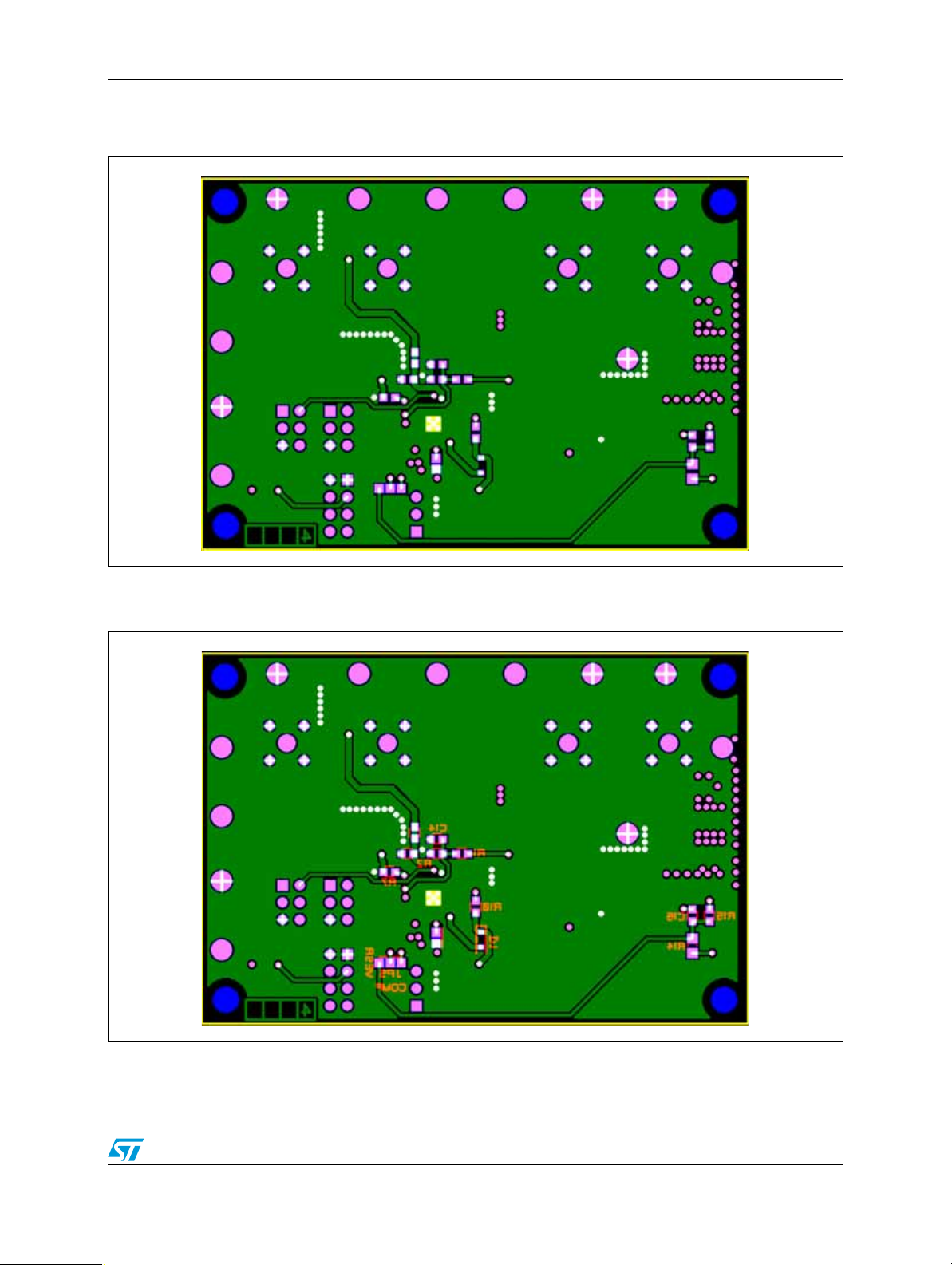
Figure 3. Topside component placement. . . . . . . . . . . . . . . . . . . . . . . . . . . . . . . . . . . . . . . . . . . . . . . 9
Figure 4. Topside view. . . . . . . . . . . . . . . . . . . . . . . . . . . . . . . . . . . . . . . . . . . . . . . . . . . . . . . . . . . . . 9
Figure 5. Layer 2 view . . . . . . . . . . . . . . . . . . . . . . . . . . . . . . . . . . . . . . . . . . . . . . . . . . . . . . . . . . . . 10
Figure 6. Layer 3 view . . . . . . . . . . . . . . . . . . . . . . . . . . . . . . . . . . . . . . . . . . . . . . . . . . . . . . . . . . . . 10
Figure 7. Bottomside view . . . . . . . . . . . . . . . . . . . . . . . . . . . . . . . . . . . . . . . . . . . . . . . . . . . . . . . . . 11
Figure 8. Bottomside component placement . . . . . . . . . . . . . . . . . . . . . . . . . . . . . . . . . . . . . . . . . . . 11
Figure 9. JP3 (MODE) setting . . . . . . . . . . . . . . . . . . . . . . . . . . . . . . . . . . . . . . . . . . . . . . . . . . . . . . 13
Figure 10. JP1 (DDRSEL) setting (change to “non-audible” in graphic) . . . . . . . . . . . . . . . . . . . . . . . 14
Figure 11. JP2 (DSCG) setting . . . . . . . . . . . . . . . . . . . . . . . . . . . . . . . . . . . . . . . . . . . . . . . . . . . . . . 14
Figure 12. JP5 (COMP) setting . . . . . . . . . . . . . . . . . . . . . . . . . . . . . . . . . . . . . . . . . . . . . . . . . . . . . . 15
Figure 13. PM6670AS test setup . . . . . . . . . . . . . . . . . . . . . . . . . . . . . . . . . . . . . . . . . . . . . . . . . . . . . 16
Figure 14. VDDQ soft-start at 180 mW load, pulse-skip mode . . . . . . . . . . . . . . . . . . . . . . . . . . . . . . 18
Figure 15. VTT turn-on (S0), pulse-skip mode. . . . . . . . . . . . . . . . . . . . . . . . . . . . . . . . . . . . . . . . . . . 18
Figure 16. VDDQ = 1.8 V, VIN = 24 V, IVDDQ = 0 A, forced PWM mode. . . . . . . . . . . . . . . . . . . . . . 19
Figure 17. VDDQ = 1.8 V, VIN = 24 V, IVDDQ = 0 A, pulse-skip mode . . . . . . . . . . . . . . . . . . . . . . . 19
Figure 18. VDDQ = 1.8 V, VIN = 24 V, no load, non-audible pulse-skip mode (33 kHz). . . . . . . . . . . 20
Figure 19. VDDQ load regulation - VIN = 24 V . . . . . . . . . . . . . . . . . . . . . . . . . . . . . . . . . . . . . . . . . . 20
Figure 20. VTT load regulation - LDOIN = VDDQ (VDDQ in forced PWM mode) . . . . . . . . . . . . . . . . 21
Figure 21. VTTREF load regulation (VDDQ in forced PWM mode). . . . . . . . . . . . . . . . . . . . . . . . . . . 21
Figure 22. VDDQ load transient (VIN = 24 V, LOAD = 0 A to 8 A at 2.5 A/µs) (pulse-skip mode). . . . 22
Figure 23. VTT load transient (VIN = 24 V, LOAD = – 2 A to 2 A at 2.5 A/µs) (pulse-skip mode). . . . 22
Figure 24. Forced PWM (blue), non-audible pulse-skip (green), pulse-skip (red) VDDQ efficiency vs. .
output current . . . . . . . . . . . . . . . . . . . . . . . . . . . . . . . . . . . . . . . . . . . . . . . . . . . . . . . . . . . 23
Figure 25. External MOS gate signals (VIN = 24 V, LOAD = 0 A) (pulse-skip mode) . . . . . . . . . . . . . 23
Figure 26. External MOS gate signals (VIN = 24 V, LOAD = 8 A) (pulse-skip mode) . . . . . . . . . . . . . 24
Figure 27. VDDQ, VTTREF, VTT output voltages and LDO input current, tracking discharge,
no load on any rail . . . . . . . . . . . . . . . . . . . . . . . . . . . . . . . . . . . . . . . . . . . . . . . . . . . . . . . 24
Figure 28. VDDQ, VTTREF and VTT, non-tracking discharge, no load on any output . . . . . . . . . . . . 25
Figure 29. UV protection, pulse-skip mode . . . . . . . . . . . . . . . . . . . . . . . . . . . . . . . . . . . . . . . . . . . . . 26
Figure 30. OV protection, pulse-skip mode . . . . . . . . . . . . . . . . . . . . . . . . . . . . . . . . . . . . . . . . . . . . . 27
Figure 31. VDDQ, VTT, VTTREF and inductor current, thermal shutdown, pulse-skip mode . . . . . . . 28
Figure 32. VDDQ current limit protection during a load transient (0 A to 10 A at 2.5 A/µs) . . . . . . . . . 29
Figure 33. VTT current limit during an output short . . . . . . . . . . . . . . . . . . . . . . . . . . . . . . . . . . . . . . . 30
Figure 34. Switching frequency vs. input voltage, VDDQ = 1.8 V, IVDDQ = 4 A, force d PWM mode. 31
Figure 35. Forced PWM (blue), non-audible pulse-skip (green) and pulse-skip (red), switching
frequency vs. output current, VDDQ = 1.8 V, VIN = 24 V. . . . . . . . . . . . . . . . . . . . . . . . . . 32
Figure 36. IVTT = 0 A, average IC temperature = 37.5 °C, max internal IC temperature = 40.1 °C . . 33
Figure 37. IVTT = 0.5 A, average IC temperature = 48.8 °C, max internal IC temperature = 54.3 °C. 34
Figure 38. IVTT = 1 A, average IC temperature = 60.5 °C, max internal IC temperature = 72.7 °C . . 35
Figure 39. IVTT = 1.5 A, average IC temperature = 73.8 °C, max internal IC temperature = 95.6 °C. 36
4/38

AN2798 Main features
1 Main features
1.1 Switching section (VDDQ)
■ 4.5 V to 36 V input voltage range
■ 0.9 V, ± 1 % voltage reference
■ 1.8 V (DDR2) or 1.5 V (DDR3) fixed output voltages
■ 0.9 V to 2.6 V adjustable output voltage
■ 1.237 V ± 1 % reference voltage available
■ Very fast load transient response constant on-time loo p control
■ No-RSENSE current sensing using low-side MOSFETs' RDSON
■ Negative current limit
■ Latched OVP, UVP and thermal shutdown
■ Fixed 3 ms soft-start
■ Selectable pulse-skipping at light load
■ Selectable non-audible (33 kHz) pulse-skip mode
■ All ceramic output capacitor applications supported
■ Output voltage ripple compensation
1.2 Reference and termination voltages (VTTREF and VTT)
■ 2 A peak LDO with foldback for VTT
■ Remote VTT output sensing
■ High-Z VTT output in S3
■ All ceramic output capacitor applications supported
■ ±15 mA low-noise buffered reference for VTTREF
5/38
Demonstration kit schematic AN2798
0
0
1
J2
V
DDQ
1
J3
PGND
1
J11
AGND
1
J1
VIN
1
J5
VCC
JP3
MODE
0
0
0
VTT
24
LDOIN
23
BOOT
22
HGATE
21
PH
ASE
20
CSNS
19
VCC
18
LGATE
17
PGND
16
PG
15
S3
14
S5
13
DSCG
12
COMP
11
MODE
10
VSNS
9
VOSCSC
8
VREFEF
7
AVCC
6
SGND5VTTR
EF
4
DDR
SEL
3
VTTSNS
2
VTTGND
1
TH
PD
25
U1
PM
6670
AS
1
J9
V
CCGND
5
4
1
6
7
8
2
3
Q2
STS7NF60L
5
4
1
6
7
8
2
3
Q1
STS5NF
60L
1
J10
AGND
1
J6
LDOIN
21
D1BABAT41J
1 2
R4 3R3
0
1
2
R3 1k 5
1
2
R1
330k
12
R2
18k
1
2
L1 1u
2 1
D2
STPSPS1L1L60A
12
C1
10u
12
C2
10u
2 1
D3
STPSPS1L1L60A
12
C3
2
20u
12
C4
2
20u
12
C10
1
2
C9
100n
12
R7
3R9
0
1 2
C21
100p
12
C19
10u
1
2
C13
1
00n
12
C20
10u
1
2
4
3
SW1
1 2
R11
100k
1 2
R12
100k
1 2
C22
100p
0
R14 7.5k
R15 6.8k
1 2
C15 47n
1 2
C16 6
80p
12
C17
0
12
C6
10u
R17 0
VCC
VCC
VCC
VCC
12
C11
10u
0
12
C8
33n
12
C14
1
00n
TP1
G
ND_TP
1
J4
PG
12
R1310100k
0
12
C5
1u
JP5
INT_CER
1 2
3 4
5 6
J
P2
DSCG
1 2
3 4
5 6
JP1
D
DRSEL
0
0
0
12
C7
10u
0
0
R8
27k
R91818k
R6
0
R10
0
12
C12
100n
1
J7
VTT
1
J8
V
TTR
EF
12
C18
1n
R16
4R7
0 0
2 Demonstration kit schematic
Figure 2. PM6670AS demonstration board schematic
DD
20
20
PG
33
00
18
ND
80
60
00
ASE
PD
10
10
10
10
100
P2
PG
AS
VS
66
EF
SEL
DDR
10
27
DR
6/38
CC
EF
TT
AM00655v1

AN2798 Demonstration kit schematic
2.1 Component list
Table 1. PM6670AS demonstration board bill of materials
Qty Component Description Package Part number MFR Value
2 C1, C2 Ceramic, 50 V, X5R, 20% SMD 1210 UMK325BJ106KM-T Taiyo Yuden 10 µ
2 C3, C4 POSCAP, 4 V, 15 m, 20% SMD 7343 (D) 4TPE220MF Sanyo 220 µ
1 C5 Ceramic, 6.3 V, X5R, 10% SMD 3216-12 Standard 1 µ
3 C6, C7, C11 Ceramic, 6.3 V, X5R, 10% SMD 0805 JMK212BJ106KG-T Taiyo Yu den 10 µ
1 C8 Ceramic, 50 V,X7R, 20% SMD 0603 Standard 33 n
C9, C10,
4
C13, C14
1 C12 Ceramic, 50 V, X7R, 10% SMD 0805 Standard 100 n
1 C15 Ceramic, 50 V, X7R, 10% SMD 0603 Standard 6n8
1 C16 Ceramic, 50 V, X7R, 10% SMD 0603 Standard 680 p
1 C17 Ceramic, 20% SMD 0603 Standard N.M.
1 C18 Ceramic, 50 V, X7R, 10% SMD 0805 Standard 1 n
2 C19, C20 Ceramic, 6.3 V, X5R, 10% SMD 0805 JMK212BJ106KG-T Taiyo Yuden N.M.
1 R1 Chip Resistor, 0.1 W, 1% SMD 0603 Standard 330 k
Ceramic, 50 V, X7R, 20% SMD 0603 Standard 100 n
1 R2 Chip Resistor, 0.1 W, 1% SMD 0603 Standard 18 k
1 R3 Chip Resistor, 0.1 W, 1% SMD 0603 Standard 1.5 k
1 R4 Chip Resistor, 0.1 W, 1% SMD 0603 Standard 3R3
1 R6 Chip Resistor, 0.1 W, 1% SMD 0805 Standard 0
1 R7 Chip Resistor, 0.1 W, 1% SMD 0603 Standard 3R9
1 R8 Chip Resistor, 0.1 W, 1% SMD 0603 Standard 39 k
1 R9 Chip Resistor, 0.1 W, 1% SMD 0603 Standard 39 k
1 R10 Chip Resistor, 0.1 W, 1% SMD 0603 Standard 0
R11, R12,
3
1 R14 Chip Resistor, 0.1 W, 1% SMD 0805 Standard 7k5
1 R15 Chip Resistor, 0.1 W, 1% SMD 0603 Standard 6k8
1 R16 Chip Resistor, 0.1 W, 1% SMD 0805 Standard 4R7
1 R17 Chip Resistor, 0.1 W, 1% SMD 0603 Standard 0
1 L1 SMT, 10.6 Arms, 4.36 mΩ 13.8 x 13.2 mm MLC1538-152ML Coilcraft 1.5 µ
1 Q1 N-Channel, 60 V SO-8 STS7NF60L ST
1 Q2 N-Channel, 60 V SO-8 STS7NF60L ST
1 D1 Schottky, 100 V, 0.2 A SOD-323 BAT41J ST
1 D2 Schottky, 60 V, 1 A DO214-AC STPS1L60A ST
1D3 N.M.
R13
Chip Resistor, 0.1 W, 1% SMD 0603 Standard 100 k
1 U1 Controller VFQFPN-24 PM6670AS ST
7/38

Demonstration kit schematic AN2798
Table 1. PM6670AS demonstration board bill of materials (continued)
Qty Component Description Package Part number MFR Value
J1, J2, J3,
J4, J5, J6,
11
J7, J8, J9,
J10,J11
JP1, JP2,
3
1 JP5 PCB pads selector
1 TP6 Test point
1 SW1 Dip switch 2 DIP-2 Standard
JP3
Header, single pin
Jumper, 2 x 3, 100 mils
8/38
AN2798 Component assembly and layout
3 Component assembly and layout
Figure 3. Topside component placement
Figure 4. Topside view
9/38
Component assembly and layout AN2798
Figure 5. Layer 2 view
Figure 6. Layer 3 view
10/38
AN2798 Component assembly and layout
Figure 7. Bottomside view
Figure 8. Bottomside component placement
11/38

I/O interface AN2798
4 I/O interface
The PM6670AS demonstration board has the following test points as given in Table 2.
Table 2. PM6670AS demonstration board input and output interface
Test point Description
VIN Battery input voltage positive terminal
PGND Battery input and VDDQ output common return
VDDQ VDDQ output
LDOIN LDO linear regulator input
VTT VTT output (LDO)
AGND VTT and VTTREF outputs common return
VTTREF VTTREF output
VCC + 5 V supply, positive terminal
VCCGND Signal ground and VCC supply return
PG VDDQ output Power Good signal
TP1 Connection point between power and signal grounds
4.1 Recommended equipment
4 V to 36 V, 30 W power supply
Active loads
Digital multimeters
200 MHz four-trace oscilloscope
12/38

AN2798 Configuration
5 Configuration
The PM6670AS board allows the user to choose the desired mode of operation using four
jumpers (JP1, JP2, JP3 and JP5) and two resistors. Refer to the following configuration
description.
5.1 JP3 fixed or adjustable output voltage (MODE pin)
The JP3 jumper is used to choose between fixed output volta ge (1.5 V or 1.8 V) and a userdefined output voltage in the range 0.9 V to 2.6 V. When connected in the lower position, the
fixed output voltage is selected and the voltage depends on the setting of the DDRSEL pin
(see Section 5.2).
If JP3 is in the upper position, the output voltage is given by:
R8 + R9
R8 + R9
×=
×=
ADJ
ADJ
9.0
9.0
R8
R8
VDDQ
VDDQ
Figure 9. JP3 (MODE) setting
Adjustable Output Voltage
Adjustable Output Voltage
Fixed Output Voltage
Fixed Output Voltage
(default position)
(default position)
Both the R8 and R9 resistors are set to 39 kΩ (1.8 V by default) and can be changed by the
user.
5.2 JP1 DDR2/DDR3 or power-saving mode (DDRSEL pin)
The JP1 jumper allows differe nt options depending on the JP3 configuration. If the fixed
output voltage is selected (JP3 in the lower position), the user can choose between 1.8 V
(DDR2) or 1.5 V (DDR3), connecting JP1 as shown in Figure 10, and the pulse-skip mode is
set by default.
When the adjustable output v oltage is selected (JP3 in the up per position), the same jumper
allows choosing between forced PWM, pulse-skip and non-audible pulse-skip modes as
shown in Figure 10 on page 14.
13/38

Configuration AN2798
Figure 10. JP1 (DDRSEL) setting
Forced PWM
Forced PWM
1.8 V output voltage
1.8 V output voltage
1.8 V output voltage
(default position)
(default position)
(default position)
1.5 V output voltage
1.5 V output voltage
1.5 V output voltage
1.5 V output voltage
1.5 V output voltage
1.5 V output voltage
JP1 options when JP3 is in the lower position
JP1 options when JP3 is in the lower position
JP1 options when JP3 is in the lower position
JP1 options when JP3 is in the upper position
JP1 options when JP3 is in the upper position
JP1 options when JP3 is in the upper position
Forced PWM
(default position)
(default position)
(default position)
Non Audible Pulse-Skip
Non Audible Pulse-Skip
Non Audible Pulse-Skip
Pulse-Skip
Pulse-Skip
Pulse-Skip
5.3 JP2 output discharge (DSCG pin)
The JP2 jumper is used to select the desired output discharge when both S3 and S5 signals
are tied low. In the upper position the outputs are not discharg ed at all, while in the lower
position the outputs are independently discharged using the internal MOSFETs (22 Ω for
VDDQ and VTT, 1.5 kΩ for VTTREF).
The tracking discharge is pr ogr amme d by putting JP2 in th e ce ntr al po sition. This di scharge
mode relies on the connection of the LDOIN pin to the VDDQ output, see Section 6: Test
setup on page 16 for details. If an external rail is used to supply the LDO, the tracking
discharge cannot be used because the device can be damaged while attempting to sink 1 A
from the LDO input.
Figure 11. JP2 (DSCG) setting
No Discharge
No Discharge
(default position)
(default position)
Tracking Discharge
Tracking Discharge
Non-Tracking Discharge
Non-Tracking Discharge
14/38

AN2798 Configuration
5.4 JP5 compensation network (COMP pin)
The JP5 jumper is located on the bottom side of the PM6670AS board an d allows
connecting the integrator input (COMP pin) to the output through a simple capacitor
(integrative compensation) or using the "virtual ESR" network for very low ESR output
capacitor applications (e.g. all ceramic output capacitor applications). The integrative
compensation is set by default.
Refer to the PM6670AS datasheet for details about ceramic output capacitor applications
and the virtual ESR design.
Figure 12. JP5 (COMP) setting
Integrative Compensation
Integrative Compensation
(default position)
(default position)
Virtual ESR Network
Virtual ESR Network
15/38
Test setup AN2798
6 Test setup
Figure 13 shows the suggested setup connections between the PM6670AS demonstration
board, the loads and the external supply. The LDO input (LDOIN) is connected to VDDQ by
default (R6 = 0 Ω).
Figure 13. PM6670AS test setup
16/38

AN2798 Getting started
7 Getting started
The following step-by-step power-up and power-down sequences are provided in order to
correctly evaluate the PM6670AS board performance.
7.1 Power-up sequence
Working in an ESD-protected environment is highly recommended. Check all wrist straps
and mat-earth connections before handling the PM6670AS board.
1. Connect power supplies as shown in the PM6670AS test setup (Figure13) and insert
the meters in order to perform the desired per formance evaluation. Conn ect the scopeprobes as desired.
2. Set the JP1 through JP5 jumpers in order to properly configure the PM6670AS board.
Set the S3-S5 switches to the on position (upper position). Do not change any of the
jumper settings when the board is po wered.
3. Set the VCC supply to 5 V ± 5 % and the current limit to 100 mA.
4. Set the VIN supply to a voltage in the range 4.5 V to 36 V. An initial test at 24 V and 3 A
current limit is suggested.
5. Set all loads to 0 A.
6. Turn on the VIN supply.
7. Turn on the VCC supply.
8. Vary the VDDQ load from 0 A to 8 A.
9. Vary the VTT load from 0 A to 2 A to test source capability. To test sink capability use
the dashed VTT load shown in Figure 13.
10. Vary the VTTREF load to test source capability.
11. Vary the VIN supply from 4.5 V to 36 V.
7.2 Power-down sequence
1. Decrease the VTTREF and VTT loads to 0 A.
2. Reduce the VDDQ load to 0.
3. Decrease the VCC supply from 5 V to 3.8 V in order to test the UVLO.
4. Increase the VCC supply from 3.8 V to 5 V to restart the device.
5. Use the S3-S5 s witches to enter/exit the S0-S3-S5 states.
6. Turn off the VDDQ load.
7. Turn off the VCC supply.
8. Turn off the VIN supply.
17/38
PM6670AS evaluation tests AN2798
8 PM6670AS evaluation tests
8.1 VDDQ, VTT and VTTREF turn-on (soft-start)
The VDDQ soft-start is divided in 4 steps. In each step the current limit is increased by ¼ of
the nominal value. This behavior is well understood by loading the rail, as performed in the
test. VTT and VTTREF soft-starts are performed at their maximum available current.
Figure 14. VDDQ soft-start at 180 mΩ load, pulse-skip mode
Figure 15. VTT turn-on (S0), pulse-s kip mode
18/38

AN2798 PM6670AS evaluation tests
8.2 VDDQ working modes
8.2.1 VDDQ forced PWM mode
When the forced PWM working mode is selected (JP3 and JP1 in the upper position), the
inductor current is allowed to become ne gative and the follo wing w avef orm can be captured.
Figure 16. VDDQ = 1.8 V, VIN = 24 V, IVDDQ = 0 A, forced PWM mode
8.2.2 VDDQ pulse-skip mode
The default working mode is the pulse-skip algorithm, in which the low-side MOSFET is
turned off when the inductor current becomes equal to zero. This behavior allows reaching
maximum efficiency.
Figure 17. VDDQ = 1.8 V, VIN = 24 V, IVDDQ = 0 A, pulse-skip mode
19/38
PM6670AS evaluation tests AN2798
8.2.3 VDDQ non-audible pulse-skip mode
In order to av oid an insufficient s witching frequency, the non-audible pulse-skip mode can be
selected (JP3 in the upper position and JP1 in the midd le). So doing, the minimum s witching
frequency allowed is 33 kHz as depicted in the following picture.
Figure 18. VDDQ = 1.8 V, VIN = 24 V, no load, non-audible pulse-skip mode (33 kHz)
8.3 VDDQ, VTT and VTTREF load regulation
Figure 19 through 21 refer to VDDQ, VTT and VTTREF output voltage versus load current.
The switching section w orks in pulse-skip mode and directly supplies VTT LDO.
Figure 19. VDDQ load regulation - VIN = 24 V
1.840
1.840
1.830
1.830
1.820
1.820
1.810
1.810
Voltage [V]
Voltage [V]
1.800
1.800
1.790
1.790
0.001 0.010 0.100 1.000 10.000
0.001 0.010 0.100 1.000 10.000
Current [A]
Current [A]
Forced PWM
Forced PWM
Pulse Skip
Pulse Skip
Non Audible PS
Non Audible PS
20/38
AN2798 PM6670AS evaluation tests
Figure 20. VTT load regulation - LDOIN = VDDQ (VDDQ in forced PWM mode)
0.930
0.930
0.920
0.920
0.910
0.910
0.900
0.900
Voltage [V]
Voltage [V]
0.890
0.890
0.880
0.880
0.870
0.870
-2.000 -1.500 -1.000 -0.500 0.000 0.500 1.000 1.500 2.000
-2.000 -1.500 -1.000 -0.500 0.000 0.500 1.000 1.500 2.000
Current [A]
Current [A]
Figure 21. VTTREF load regulation (VDDQ in forced PWM mode)
0.920
0.920
0.915
0.915
0.910
0.910
0.905
0.905
Voltage [V]
Voltage [V]
0.900
0.900
0.895
0.895
0.890
0.890
-30 -20 -10 0 10 20 30
-30 -20 -10 0 10 20 30
Current [mA]
Current [mA]
21/38
PM6670AS evaluation tests AN2798
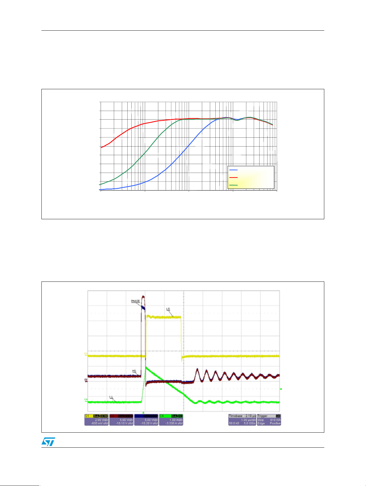
8.4 VDDQ and VTT load transient responses
Load transient responses are evaluated by loading VDDQ and VTT output rails with a
current slew rate of 2.5 A/µs.
Figure 22. VDDQ load transient (VIN = 24 V, LOAD = 0 A to 8 A at 2.5 A/µs) (pulse-skip mode)
Figure 23. VTT load transient (VIN = 24 V, LOAD = – 2 A to 2 A at 2.5 A/µs) (pulse-skip mode)
22/38
AN2798 PM6670AS evaluation tests
8.5 VDDQ efficiency
The three working modes lead to different power efficiency. The test setup is VIN = 24 V,
FSW = 330 kHz, VDDQ = 1.8 V. The following graph summarizes the results.
Figure 24. Forced PWM (blue), non-audible pulse-skip (green), pulse-skip (red) VDDQ efficiency
vs. output current
100
100
90
90
80
80
70
70
60
60
50
50
40
40
Efficiency [%]
Efficiency [%]
30
30
20
20
10
10
0
0
0.001 0.010 0.100 1.000 10.000
0.001 0.010 0.100 1.000 10.000
Current [A]
Current [A]
Forced PWM
Forced PWM
Pulse Skip
Pulse Skip
Non Audible PS
Non Audible PS
8.6 VDDQ gate drivers
The PM6670 internal MOS driver turns on and off the high-side and low-side external
MOSFET, avoiding cross-conduction. In Figure 24 and 25 the gates signals are depicted
without load and with load.
Figure 25. External MOS gate signals (VIN = 24 V, LOAD = 0 A) (pulse-skip mode)
23/38
PM6670AS evaluation tests AN2798
Figure 26. External MOS gate signals (VIN = 24 V, LOAD = 8 A) (pulse-skip mode)
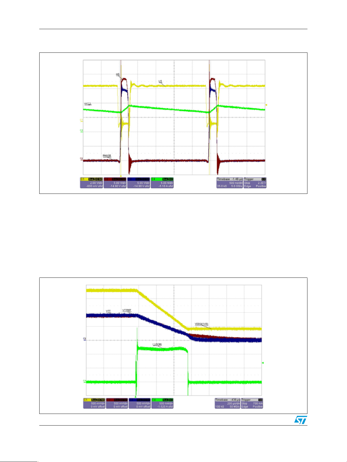
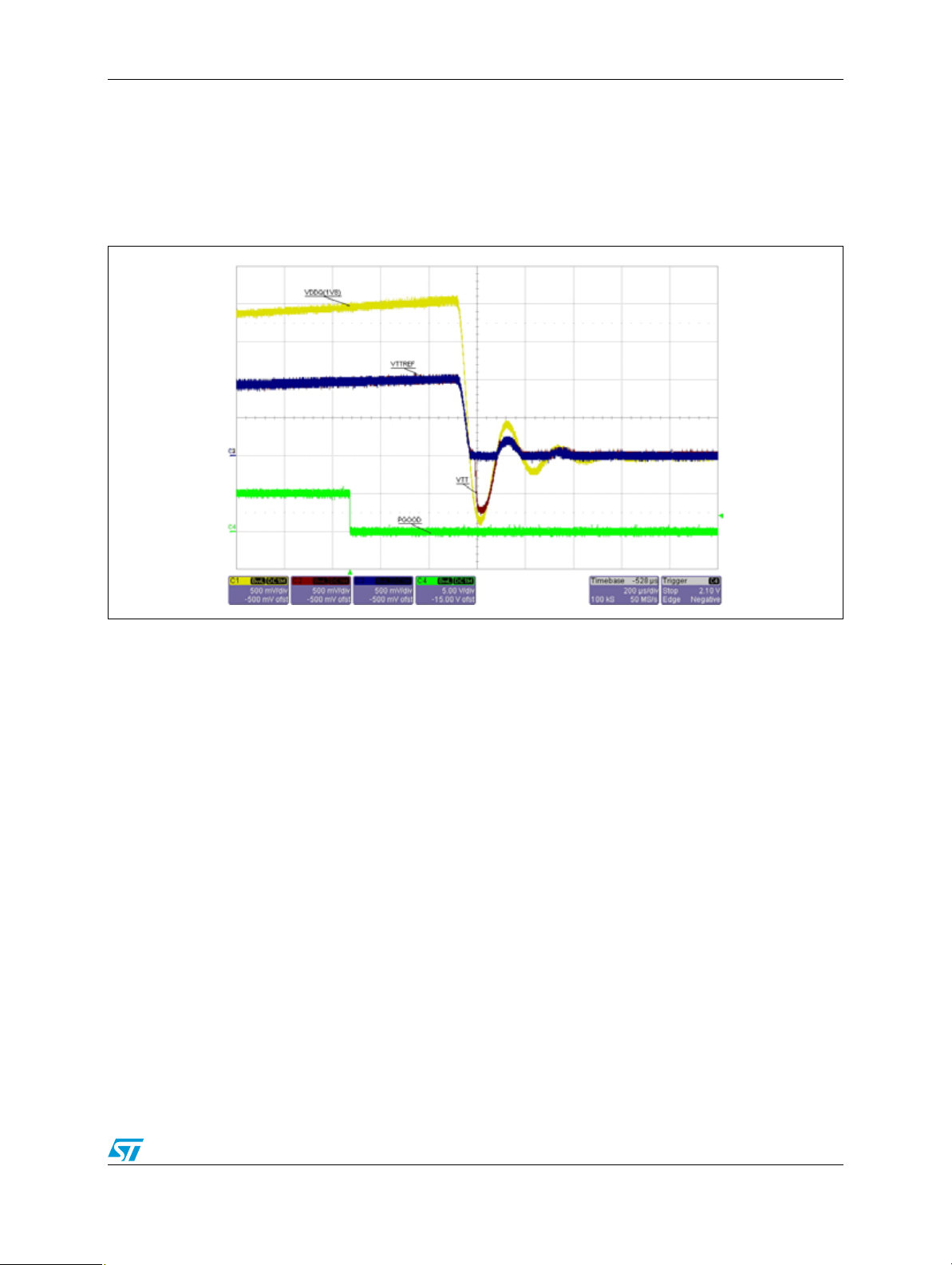
8.7 VDDQ, VTT and VTTREF turnoff (soft-end)
Tracking discharge
The jumper JP2, if placed in the middle, a llows the output tracking discharge. When S3 and
S5 are pulled down, VTT discharges VDDQ b y sinking 1 A and, at the same ti me , tra c ks the
VDDQ remaining half. When VDDQ reaches abou t 400 mV, the output discharge MOSFETs
are all closed and each rail is finally discharged.
Figure 27. VDDQ, VTTREF, VTT output voltages and LDO input current, tracking discharge, no
load on any rail
24/38

AN2798 PM6670AS evaluation tests
Table 3. Measured discharge resistance in soft-discharge mode
VDDQ output VTTREF output VTT output
Measured N.T.D. discharge
MOSFET’s RDSon
25 Ω 1.5 kΩ 23 Ω
Non-tracking discharge
When the non-tracking discharge is programmed (JP2 in the lower position) and S3-S5 are
both tied to GND , each out put rail is discharged through its discharge MOSFET, as depicted
in the following picture.
Figure 28. VDDQ, VTTREF and VTT, non-tracking discharge, no load on any output
25/38

PM6670AS evaluation tests AN2798
8.8 UV, OV and thermal protections
Latched UV protection
If the output voltage is lower than the 70 % nominal value, the undervoltage sta te is ent ered
and the discharge MOSFETs are turned on (as in the non-tracking soft-end).
Figure 29. UV protection, pulse-skip mode
26/38
AN2798 PM6670AS evaluation tests
Latched OV protection
If the output voltage is hig her than the 115 % nomin al va lue, the o v ervoltage state is e ntered
and the low-side MOSFET is turned on. VTT and VTTREF are discharged through thei r
discharge MOSFETs.
Figure 30. OV protection, pulse-skip mode
27/38

PM6670AS evaluation tests AN2798
Latched thermal shutdown
If the junction temperature rises up to 150 deg, the thermal protection circuit turns off the
device and discharges the output rails by performing the non-tracking discharge soft-end.
Figure 31. VDDQ, VTT, VTTREF and inductor current, thermal shutdown, pulse-skip mode
8.9 VDDQ current limit
The valley current limit avoids any high side turning on if the inductor current is higher than
the programmed value. This current limit can be designed with the following equation:
The current sensing is performed by comparing the voltage drop in the low-side MOSFET,
during the TOFF period, with the voltage drop given by an injected current and the current
limit resistor.
I
I
CL
CL
100µA x
100µA x
=
=
R
R
R
R
ILIM
ILIM
DSonLS
,
DSonLS
,
28/38

AN2798 PM6670AS evaluation tests
Figure 32. VDDQ current limit protection during a load transient (0 A to 10 A at 2.5 A/µs)
29/38

PM6670AS evaluation tests AN2798
8.10 VTT current limit (foldback)
VTT LDO has a foldback pro tection feature which reduces the current limit to 1 A when the
VTT output voltage is outside the ± 10 % Power Good window. The current limit is restored
to 2 A when the output voltage re-enters the Power Good window.
Figure 33. VTT current limit during an output short
30/38

AN2798 PM6670AS evaluation tests
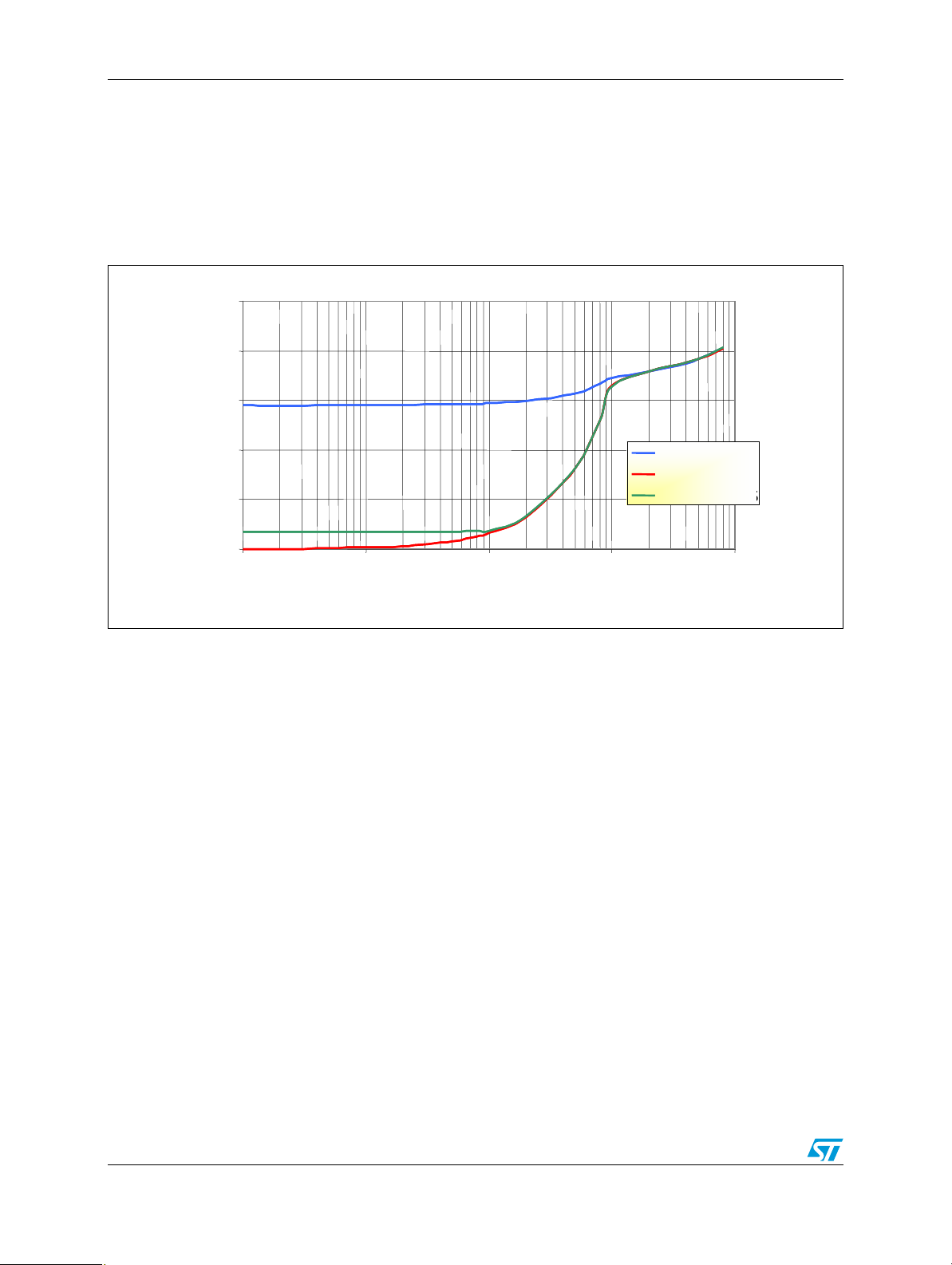
8.11 Switching frequency
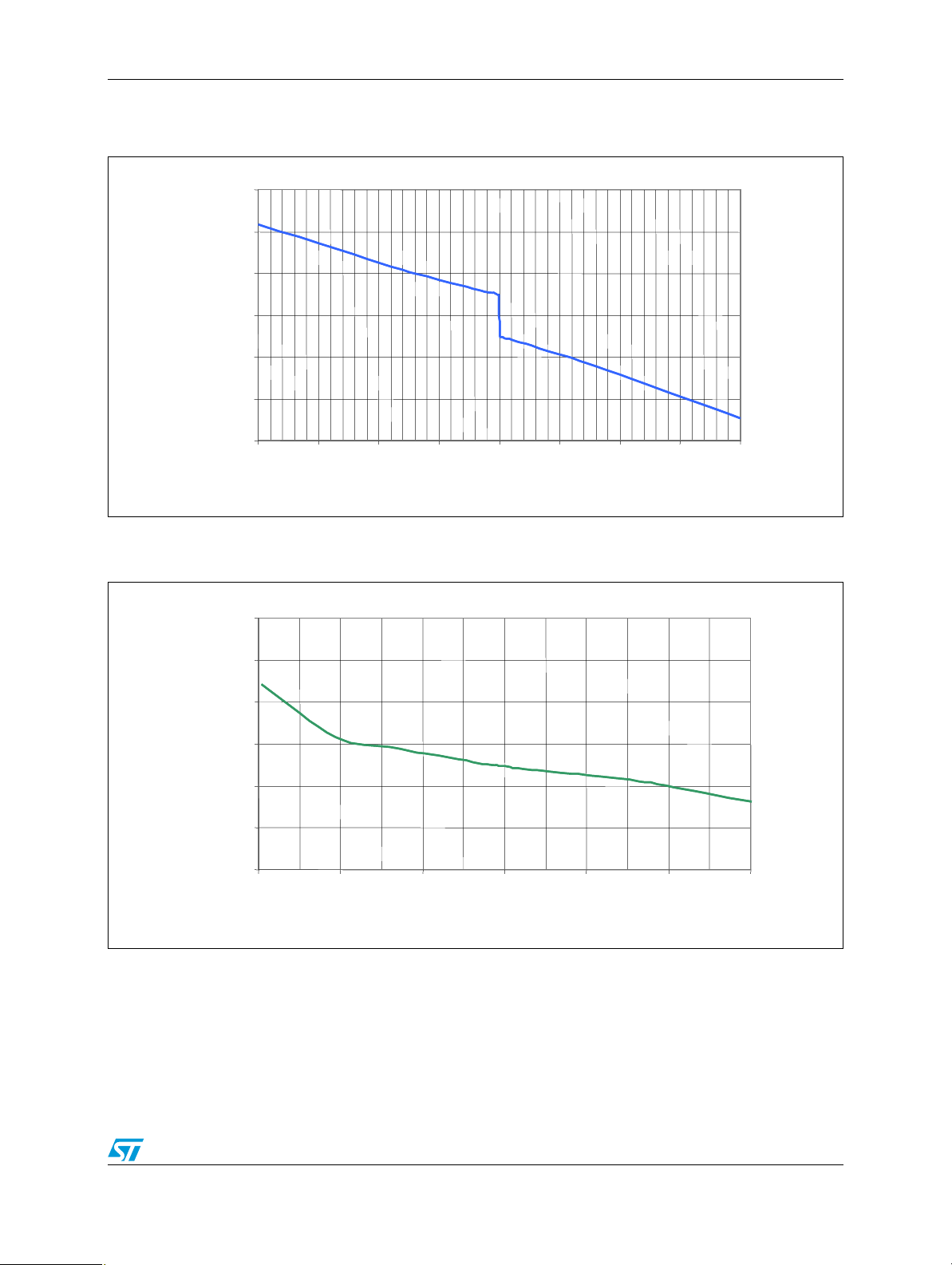
Switching frequency vs. input voltage
The constant on-time controller leads to a quasi-constant switching frequency, slightly
following the input voltage.
Figure 34. Switching frequency vs. input voltage, VDDQ = 1.8 V, IVDDQ = 4 A, forced PWM mode
500
500
450
450
400
400
Frequency [kHz]
Frequency [kHz]
350
350
300
300
4142434
4142434
Voltage [V]
Voltage [V]
31/38
PM6670AS evaluation tests AN2798
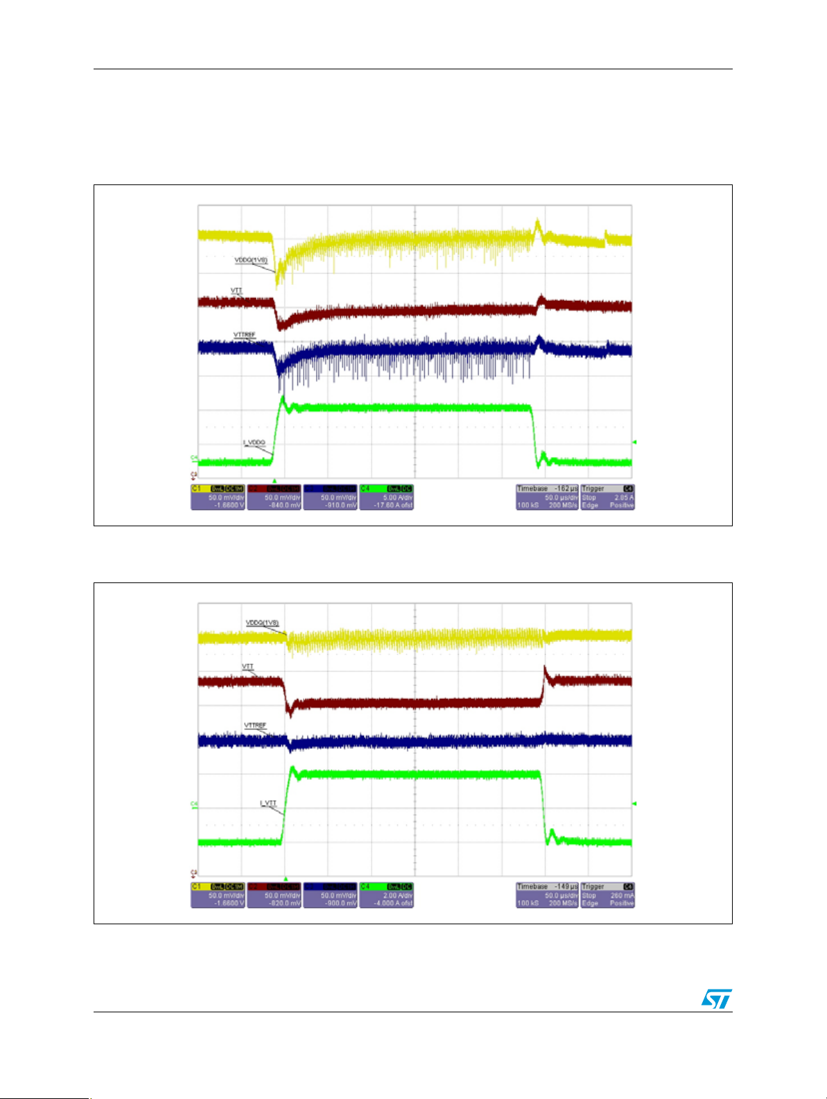
Switching frequency vs. output current
The switching frequency can decrease to very low values in pu lse-skip mode instea d in nonaudible pulse-skip there is a lower limit (about 33 kHz). With increasing load, however, the
switching frequency increa ses a bit, as a consequence of conduction and switching losses.
Figure 35. Forced PWM (blue), non-audible pulse-skip (green) and pulse-skip (red), switching
frequency vs. output current, VDDQ = 1.8 V, VIN = 24 V
500
500
400
400
300
300
200
200
Frequency [kHz]
Frequency [kHz]
100
100
Forced PWM
Forced PWM
Pulse Skip
Pulse Skip
Non Audible PS
Non Audible PS
0
0
0.001 0.010 0.100 1.000 10.000
0.001 0.010 0.100 1.000 10.000
Current [A]
Current [A]
32/38
AN2798 PM6670AS evaluation tests
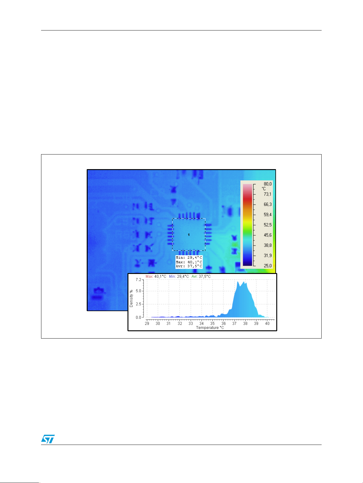
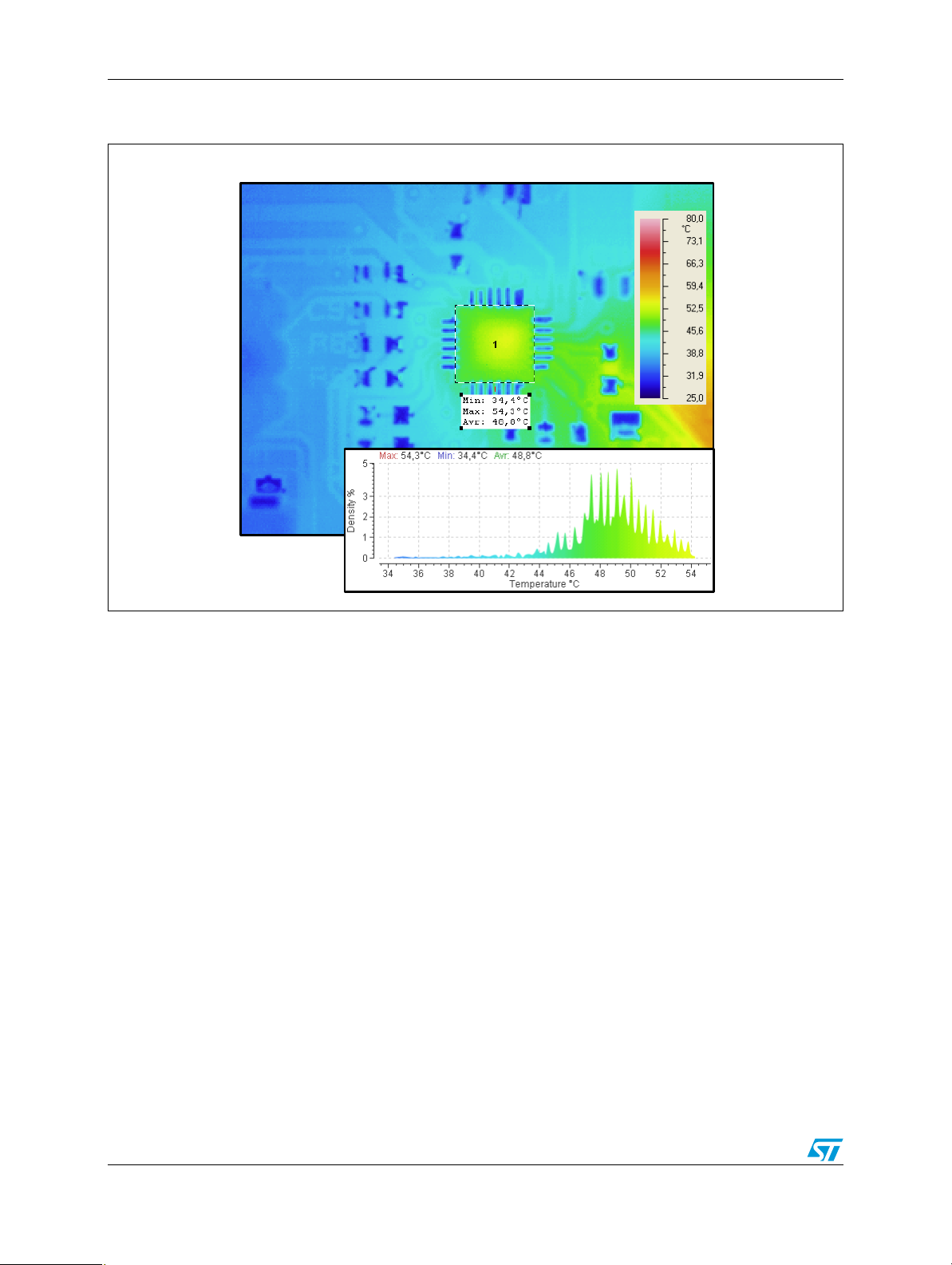
8.12 Thermal behavior
The IC internal maximum and average temperature can be monitored by an IR camera. For
the measurements in Figure 36 through 39 the test setup is:
● V
● F
● Pulse-skip mode
● I
● VTT rail powered by VDDQ
● T
By increasing the VTT current, the IC temperature changes as depicted in the following
pictures.
= 24 V
IN
= 360 kHz
SW
VDDQ
AMB
= 4 A
= 25 °C
Figure 36. I
= 0 A, average IC temperature = 37.5 °C, max internal IC temperature = 40.1 °C
VTT
33/38
PM6670AS evaluation tests AN2798
Figure 37. I
= 0.5 A, average IC temperature = 48.8 °C, max internal IC temperature = 54.3 °C
VTT
34/38
AN2798 PM6670AS evaluation tests
Figure 38. I
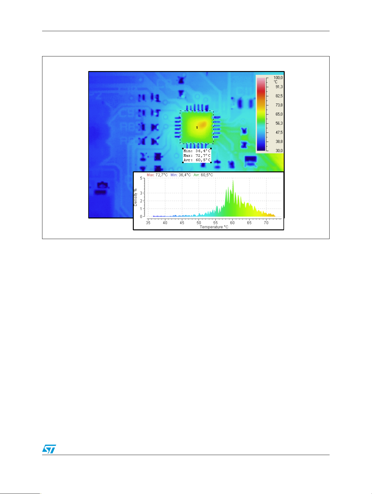
= 1 A, average IC temperature = 60.5 °C, max internal IC temperature = 72.7 °C
VTT
35/38

PM6670AS evaluation tests AN2798
Figure 39. I
= 1.5 A, average IC temperature = 73.8 °C, max internal IC temperature = 95.6 °C
VTT
36/38

AN2798 Revision history
9 Revision history
Table 4. Document revision history
Date Revision Changes
04-Nov-2008 1 Initial release.
37/38

AN2798
Please Read Carefully:
Information in this document is provided solely in connection with ST products. STMicroelectronics NV and its subsidiaries (“ST”) reserve the
right to make changes, corrections, modifications or improvements, to this document, and the products and services described herein at any
time, without notice.
All ST products are sold pursuant to ST’s terms and conditions of sale.
Purchasers are solely res ponsibl e fo r the c hoic e, se lecti on an d use o f the S T prod ucts and s ervi ces d escr ibed he rein , and ST as sumes no
liability whatsoever relati ng to the choice, selection or use of the ST products and services described herein.
No license, express or implied, by estoppel or otherwise, to any intellectual property rights is granted under this document. If any part of this
document refers to any third pa rty p ro duc ts or se rv ices it sh all n ot be deem ed a lice ns e gr ant by ST fo r t he use of su ch thi r d party products
or services, or any intellectua l property c ontained the rein or consi dered as a warr anty coverin g the use in any manner whats oever of such
third party products or servi ces or any intellectual property contained therein.
UNLESS OTHERWISE SET FORTH IN ST’S TERMS AND CONDITIONS OF SALE ST DISCLAIMS ANY EXPRESS OR IMPLIED
WARRANTY WITH RESPECT TO THE USE AND/OR SALE OF ST PRODUCTS INCLUDING WITHOUT LIMITATION IMPLIED
WARRANTIES OF MERCHANTABILITY, FITNESS FOR A PARTICUL AR PURPOS E (AND THEIR EQUIVALE NTS UNDER THE LAWS
OF ANY JURISDICTION), OR INFRINGEMENT OF ANY PATENT, COPYRIGHT OR OTHER INTELLECTUAL PROPERTY RIGHT.
UNLESS EXPRESSLY APPROVED IN WRITING BY AN AUTHORIZED ST REPRESENTATIVE, ST PRODUCTS ARE NOT
RECOMMENDED, AUTHORIZED OR WARRANTED FOR USE IN MILITARY, AIR CRAFT, SPACE, LIFE SAVING, OR LIFE SUSTAINING
APPLICATIONS, NOR IN PRODUCTS OR SYSTEMS WHERE FAILURE OR MALFUNCTION MAY RESULT IN PERSONAL INJ URY,
DEATH, OR SEVERE PROPERTY OR ENVIRONMENTAL DAMAGE. ST PRODUCTS WHICH ARE NOT SPECIFIED AS "AUTOMOTIVE
GRADE" MAY ONLY BE USED IN AUTOMOTIVE APPLICATIONS AT USER’S OWN RISK.
Resale of ST products with provisions different from the statements and/or technical features set forth in this document shall immediately void
any warranty granted by ST fo r the ST pro duct or serv ice describe d herein and shall not cr eate or exten d in any manne r whatsoever, any
liability of ST.
ST and the ST logo are trademarks or registered trademarks of ST in various countries.
Information in this document su persedes and replaces all information previously supplied.
The ST logo is a registered trademark of STMicroelectronics. All other names are the property of their respective owners.
© 2008 STMicroelectronics - All rights reserved
STMicroelectronics group of compan ie s
Australia - Belgium - Brazil - Canada - China - Czech Republic - Finland - France - Germany - Hong Kong - India - Israel - Italy - Japan -
Malaysia - Malta - Morocco - Singapore - Spain - Sweden - Switzerland - United Kingdom - United States of America
www.st.com
38/38
 Loading...