

Page 1
Super wide-range buck converter based on the VIPer16
1 Introduction
This document describes the STEVAL-ISA010V1 demonstration board, which is designed
as an example of a simple non-isolated auxiliary power supply for a range of input voltages
from 85 VAC to 500 VAC.
There is an ever-increasing demand for small power supplies capable of working without
voltage range limitations, even at nominal levels of 400 VAC and 415 VAC, respectively. The
real voltage levels can reach 500 VAC (415 V + 20%). The major markets for this type of
SMPS are home appliances and metering.
The new STMicroelectronics™ family of monolithic converters is well-suited for this range of
input voltages, thanks to the 800 V avalanche-rugged MOSFET integrated within the same
package with the control chip. This application note describes a low power SMPS with
a buck topology using STMicroelectronics’ VIPer16 fixed-frequency off-line converter as
a main circuit. The VIPer16 device includes an 800 V rugged power switch, a PWM
controller, programmable overcurrent, overvoltage, overload, a hysteretic thermal protection,
soft-start and safe auto-restart after any fault condition removal. Burst mode operation at
light load combined with the very low consumption of the device helps to meet standby
energy-saving regulations. The significant benefit of this new chip derives from the jitter of
the switching frequency and the possibility to supply the chip directly from the DC HV bus,
so auxiliary supply is not mandatory. The VIPer16 is suitable for flyback or buck topologies,
and thanks to an internal self-supply circuit it does not require an auxiliary supply.
AN2872
Application note
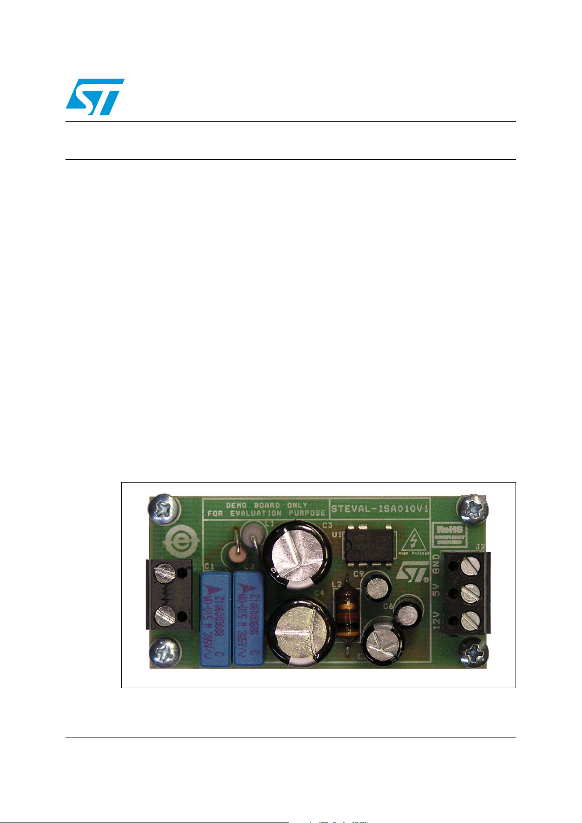
Figure 1. The STEVAL-ISA010V1 demonstration board
April 2009 Doc ID 15305 Rev 1 1/23
www.st.com
Page 2

Contents AN2872
Contents
1 Introduction . . . . . . . . . . . . . . . . . . . . . . . . . . . . . . . . . . . . . . . . . . . . . . . . 1
2 Main characteristics . . . . . . . . . . . . . . . . . . . . . . . . . . . . . . . . . . . . . . . . . 5
3 Description . . . . . . . . . . . . . . . . . . . . . . . . . . . . . . . . . . . . . . . . . . . . . . . . . 6
3.1 Theory of operation . . . . . . . . . . . . . . . . . . . . . . . . . . . . . . . . . . . . . . . . . . 6
3.1.1 The basic principle of the buck converter . . . . . . . . . . . . . . . . . . . . . . . . 6
3.1.2 Practical aspects of a buck converter dedicated for mains
and 3-phase input . . . . . . . . . . . . . . . . . . . . . . . . . . . . . . . . . . . . . . . . . . 7
3.2 Converter schematic . . . . . . . . . . . . . . . . . . . . . . . . . . . . . . . . . . . . . . . . . 9
3.3 PCB . . . . . . . . . . . . . . . . . . . . . . . . . . . . . . . . . . . . . . . . . . . . . . . . . . . . . 11
3.4 Bill of material . . . . . . . . . . . . . . . . . . . . . . . . . . . . . . . . . . . . . . . . . . . . . . 12
4 Experimental results . . . . . . . . . . . . . . . . . . . . . . . . . . . . . . . . . . . . . . . . 13
4.1 Load regulation and output voltage ripple . . . . . . . . . . . . . . . . . . . . . . . . 13
4.2 Standby . . . . . . . . . . . . . . . . . . . . . . . . . . . . . . . . . . . . . . . . . . . . . . . . . . 14
4.3 Efficiency . . . . . . . . . . . . . . . . . . . . . . . . . . . . . . . . . . . . . . . . . . . . . . . . . 16
4.4 MOSFET voltage stress . . . . . . . . . . . . . . . . . . . . . . . . . . . . . . . . . . . . . . 16
4.5 Short-circuit behavior . . . . . . . . . . . . . . . . . . . . . . . . . . . . . . . . . . . . . . . . 17
4.6 EMC . . . . . . . . . . . . . . . . . . . . . . . . . . . . . . . . . . . . . . . . . . . . . . . . . . . . . 18
4.6.1 Surge - IEC 61000-4-5 . . . . . . . . . . . . . . . . . . . . . . . . . . . . . . . . . . . . . . 18
4.6.2 Burst - IEC 61000-4-4 . . . . . . . . . . . . . . . . . . . . . . . . . . . . . . . . . . . . . . 19
4.6.3 EMI . . . . . . . . . . . . . . . . . . . . . . . . . . . . . . . . . . . . . . . . . . . . . . . . . . . . 19
4.7 Thermal behavior . . . . . . . . . . . . . . . . . . . . . . . . . . . . . . . . . . . . . . . . . . . 20
5 Conclusion . . . . . . . . . . . . . . . . . . . . . . . . . . . . . . . . . . . . . . . . . . . . . . . . 21
6 References . . . . . . . . . . . . . . . . . . . . . . . . . . . . . . . . . . . . . . . . . . . . . . . . 21
7 Revision history . . . . . . . . . . . . . . . . . . . . . . . . . . . . . . . . . . . . . . . . . . . 22
2/23 Doc ID 15305 Rev 1
Page 3

AN2872 List of tables
List of tables
Table 1. List of components . . . . . . . . . . . . . . . . . . . . . . . . . . . . . . . . . . . . . . . . . . . . . . . . . . . . . . . 12
Table 2. Temperature of the VIPer16 at full load . . . . . . . . . . . . . . . . . . . . . . . . . . . . . . . . . . . . . . . 20
Table 3. Document revision history . . . . . . . . . . . . . . . . . . . . . . . . . . . . . . . . . . . . . . . . . . . . . . . . . 22
Doc ID 15305 Rev 1 3/23
Page 4

List of figures AN2872
List of figures
Figure 1. The STEVAL-ISA010V1 demonstration board . . . . . . . . . . . . . . . . . . . . . . . . . . . . . . . . . . . 1
Figure 2. Buck converter schematic. . . . . . . . . . . . . . . . . . . . . . . . . . . . . . . . . . . . . . . . . . . . . . . . . . . 6
Figure 3. Standard implementation of a buck converter with a monolithic device . . . . . . . . . . . . . . . . 8
Figure 4. Schematic of the step-down converter based on the VIPer16L . . . . . . . . . . . . . . . . . . . . . . 9
Figure 5. PCB layout of the buck converter (top, bottom, bottom layout) . . . . . . . . . . . . . . . . . . . . . 11
Figure 6. 12 V output load regulation for different output loads and input voltage levels
(linear regulator U2 not assembled) . . . . . . . . . . . . . . . . . . . . . . . . . . . . . . . . . . . . . . . . . . 13
Figure 7. Output voltage ripple for different input voltages . . . . . . . . . . . . . . . . . . . . . . . . . . . . . . . . 14
Figure 8. Alternative schematic of the input part using balancing Zener diodes instead of
resistors . . . . . . . . . . . . . . . . . . . . . . . . . . . . . . . . . . . . . . . . . . . . . . . . . . . . . . . . . . . . . . . 15
Figure 9. Standby consumption for different input voltage levels . . . . . . . . . . . . . . . . . . . . . . . . . . . 15
Figure 10. Efficiency of the converter . . . . . . . . . . . . . . . . . . . . . . . . . . . . . . . . . . . . . . . . . . . . . . . . . 16
Figure 11. Drain voltage (CH1) and inductor current (CH4) at different input voltages . . . . . . . . . . . . 17
Figure 12. Indication of current (CH4) and drain voltage (CH1) during short-circuit . . . . . . . . . . . . . . 18
Figure 13. EMI measurements of the demonstration board. . . . . . . . . . . . . . . . . . . . . . . . . . . . . . . . . 20
4/23 Doc ID 15305 Rev 1
Page 5

AN2872 Main characteristics
2 Main characteristics
The main characteristics of the SMPS are listed below:
●
Input:
–V
– f: 45 - 66 Hz
●
Output:
– 12 V ± 10%
–5 V ± 4%
– 150 mA total (5 V and 12 V output) output current for full input voltage range
●
Standby: 96 mW at 230 VAC
●
Short-circuit: protected
●
PCB type and size:
–FR4
– Single side 70 µm
– 27 x 45 mm
●
Isolation: non isolated - N connected to output GND
●
EMI: In accordance with EN55022 - class B
●
EMC: Surge - IEC 61000-4-5 - 2 kV
●
EMC: Burst - IEC 61000-4-4 - 8 kV
: 85 - 500 VAC
IN
Doc ID 15305 Rev 1 5/23
Page 6
Description AN2872
3 Description
3.1 Theory of operation
The detailed calculation and principles of the buck converter for mains voltage operating
range is described in Section 6: References:1. and References:2. The basic ideas and most
important behaviors of the buck converter for mains applications is described in the chapters
that follow.
3.1.1 The basic principle of the buck converter
The schematic of the buck converter is shown in Figure 2. During the ON time, the control
circuit makes the high side switch T
output capacitor C
during the ON time. Assuming the voltage across C2 is constant and the
2
input voltage is constant, the voltage drop over L
over the inductor causes a linear increase in the current through inductor L
the inductor current is proportional to the inductance of the inductor and the level of voltage
drop over the inductor.
Figure 2. Buck converter schematic
conduct. The input DC voltage is connected to L1 and
1
is constant (V1 - V2). The constant voltage
1
. The slope of
1
Control
L
L
T1
C
V
1
1
1
+
+
D
1
–
I
L
C
2
V
V
1
2
Control
L
T
T
1
C
1
D
D
1
1
+
–
+
C
I
I
L
2
ON time OFF time
I
V
L
After T
L
t
t
is switched OFF, the low side switch (diode D1) conducts. If we assume, for
1
∆I
I
L
t
V
L
t
AM00359
simplification purposes, the voltage drop over the diode is zero, then the voltage drop over
inductor L
is equal to the output voltage (voltage drop over C2). Because the voltage across
1
the inductor is different (compare ON time), the slope of inductor current is also different.
The behavior of a buck converter can be expressed by Equation 1.
Equation 1
V
∆I
V2–()t
1
-------- --------- ---------- ------
ON
L
V2t
OFF
--------- ---------==
L
6/23 Doc ID 15305 Rev 1
Page 7

AN2872 Description
The regulator of the circuit measures the output voltage, compares it with the reference
voltage and modifies the duration of the ON time to keep the output voltage constant.
In cases where the inductor current is operating in the continuous mode (the current does
not cross zero at full load) the duty cycle can be obtained using Equation 2. This formula
follows from Equation 1. Another method to obtain Equation 2 is to consider the buck
converter as a low pass filter (L
, C2), connected to a rectangular signal and that the low
1
pass filter generates a mean value.
Equation 2
V
------=
V
2
1
δ
3.1.2 Practical aspects of a buck converter dedicated for mains and 3-phase
input
The application of a mains or 3-phase buck converter using a simple monolithic device
results in several special conditions. A few of the most important are described in the
following paragraphs.
The operation of a buck converter such as that of the diagram in Figure 2 requires an active
high side switch. Therefore, the monolithic device (with integrated N-channel MOSFET) is
also connected on the high side (between + of bulk capacitor and inductor). The GND of the
controller connected to the source of the MOSFET refers to the high side of the inductor
(see Figure 3). This wiring of circuit causes the feedback signal not to be directly sensed
from the output due to the shift of the GND of output voltage and controller. Basically, there
are two ways to move the information regarding the output voltage from the output to the
controller. The first way is to apply an optocoupler between the output and the converter.
The additional error amplifier and reference (typically TL431 or a simple Zener diode) must
be assembled to drive the LED of the optocoupler. This method gives high precision of the
output voltage level and low load regulation. However, it also increases the cost and space
requirements. The second principle is to use a replica of the output voltage stored in the
auxiliary capacitor during OFF time. The schematic in Figure 3 shows the principle
connection of the components. The auxiliary capacitor C
from inductor L
voltage drop over both capacitors (C
to the same voltage level as capacitor C2. It can be expected that the
1
and C3) must be equal. However, in real applications
2
the voltages are not exactly the same. This difference is caused by the difference in the
discharge current of capacitors, different capacitance and different voltage drop on diodes
D
and D2. An important effect of the variance of the voltage drop of C2 and C3 is the fact
1
that only C
is charged during ON time. Due to this behavior it is possible to see a
2
theoretically unlimited increase in the output voltage at light or no load, because the energy
delivered during the ON time is higher than the total energy required by the load. Therefore,
an additional load (resistor) or voltage limiter (Zener diode) is required on the output to
protect the output capacitor and the load against overvoltage at light load.
is charged during the OFF time
3
Doc ID 15305 Rev 1 7/23
Page 8

Description AN2872
Figure 3. Standard implementation of a buck converter with a monolithic device
Control
V
C
1
1
T1
FB
GND
C
3
D
1
D
2
L
1
C
V
2
2
AM00360
The second important behavior of a buck converter dedicated for mains applications follows
from the ratio between the input and output voltage. As derived from Equation 2 the duty
cycle is very low when the ratio between the input and output is very high. This also means
the ON time must be very short. It is possible for the ON time required for correct operation
to be shorter than the minimum ON time of the controller defined in the datasheet (the
maximum duration of the minimum ON time of the VIPer16 is 450 ns. see Section 6: 3). In
this case the SMPS delivers more energy than the controller, which is compensated by the
skipping of some pulses. This leads to higher ripple of the output voltage. This effect can be
compensated by applying a higher inductance value and a lower switching frequency.
The last technical point discussed in this paragraph concerns the input bulk capacitor in
applications dedicated to very high input AC voltage. In this case, the input voltage is up to
500 VAC. The DC voltage can reach voltage levels of up to 707 VDC. The input bulk
capacitor must be able to sustain such voltage levels. Unfortunately, there are no standard
aluminum capacitors on the market suitable for this voltage, so two capacitors connected in
series have been applied.
The series connection of two capacitors has two effects on the voltage drop over each
capacitor. The first is an influence over the tolerance of the capacitance and the second is
an influence over the leakage current.
Regarding the tolerance, the worst case is that one capacitor’s capacitance is at the
maximum upper limit and the second at the lower limit. Equation 3 defines the voltage
distribution on each capacitor for this configuration:
Equation 3
V
MAX
V
C1 C2,
------- -------
2
1 δ±()=
where
V
is the voltage across the capacitor with higher capacitance (the sign "–" in the brackets)
C1
is the voltage drop on the capacitor with lower capacitance (the sign "+" in the brackets)
V
C2
is the DC voltage bus
V
MAX
δ is the tolerance of the capacitors expressed as a percentage
If the voltage bus is 707 V and the tolerance is 20%, the highest possible voltage across the
capacitor is 424 VDC. Therefore, for this voltage range, the use of 450 V capacitors is
recommended.
The leakage current can cause additional unbalancing of the voltages and an increase in
the voltage drop of one capacitor over the allowed limit. If the leakage currents of both
8/23 Doc ID 15305 Rev 1
Page 9

AN2872 Description
capacitors are the same, no problem is presented. But in cases where there is a difference
in leakage currents (which is the case in practical applications) this difference will cause the
capacitor with lower leakage to be charged by this difference and the voltage over this
capacitor will rise, risking exceeding the voltage defined in the datasheet. To avoid this
effect, so-called balancing resistors are applied parallel to the electrolytic capacitors. The
correct value of the balancing resistors can be calculated from the difference in the leakage
currents and applied voltage. Unfortunately, the maximum difference in leakage currents is
not defined. It is possible, however, that the calculations for the balancing resistors are
available the technical documentation of some aluminum capacitor manufactures. An
examination of these documents reveals that there is not a single method and each
manufacturer uses different calculation methods, each of which unfortunately can give very
different values. Technical notes describing the calculations of balancing resistors can be
found in Section 6: References: 4, 5, 6, 7. Typically, the value of balancing resistors is in the
range of hundreds of kΩ to several MΩ.
The drawback of using balancing resistors is the constant input load. The additional
constant load caused by balancing resistors is mainly visible in the standby consumption
and reduction of efficiency at low power SMPS. It is recommended to set the value of the
balancing resistors to the maximum level, respecting the technical recommendations of the
manufacturer of the aluminum capacitors selected.
3.2 Converter schematic
The schematic of the converter is shown in Figure 4. It consists of three sections: an input,
a high voltage DC-DC converter and a linear regulator.
The input sections integrates a rectifier (D
C
, L1, C3, C4), protection (R1) and bulk capacitors (C3, C4) which store energy for the DC-
2
DC converter when the input voltage is low. Because there is 500 VAC applied, which
means a DC level over 700 V, the foil and electrolytic capacitors are connected in series.
This is due to the fact that the standard foil safety capacitors are produced for 440 VAC, and
the maximum DC voltage for standard electrolytic capacitors is 450 V. As the electrolytic
capacitors have different leakage current, the balancing resistors (R
applied to guarantee that the voltage of each capacitor does not exceed the maximum rating
even at maximum input voltage.
Figure 4. Schematic of the step-down converter based on the VIPer16L
D
D
1N4007
J
1
85 - 500 VAC
C
2
150 nF / X2
1
C
150 nF / X2
R122 Ω
4
3
1N4007
1
2
L12.2 mH
R
750 kΩ
2
10 µF / 450 V
R
5 750 kΩ
R6750 kΩ
R8750 kΩ
C
3
7
8
C
4
10 µF /
450 V
U1VIPer16
Drain
Drain
COMP5LIM
3
C
7 1.8 nF
, D4) of the input RMS voltage, an EMI filter (C1,
3
D11N4148
R
FB
V
DD
4
2
1
S
R7N.A.
R
C
9
10 µF
/ 35V
1 kΩ
9
3
24 kΩ
R
4
9.1 kΩ
D
5
STTH108
D
2
STTH108
C
8
100 nF
1 mH
L
2
D
15 V
, R5, R6, R8) must be
2
U2L78L05
3 1
V
V
OUT
IN
C
5
220 µF
/ 25 V
GND
2
6
C
6
10 µF
/ 35 V
J
2
1
2
3
Output
AM00361
The high voltage DC-DC section is a buck converter based on the VIPer16. It converts the
input high DC voltage stored in capacitors C
Doc ID 15305 Rev 1 9/23
and C4 to output. The high side switch is
3
Page 10

Description AN2872
a MOSFET integrated in the VIPer16. The low side switch of the buck converter is
freewheeling diode D
C
during the ON time, when the MOSFET is conducting. The ON time (and consequently
5
(800 V / 1 A). The energy is saved in inductor L2 and output capacitor
5
also the duty cycle) is very short (in the range several %) due to the high ratio between the
input and the output voltage. During the OFF time, the MOSFET is switched OFF and diode
D
conducts. Inductor L2 is discharged to the output and to capacitors C5 and C8 through
5
diodes D
voltage drop over C
Diode D
and D5. As the inductor L2 is, during OFF time, connected to C8 and C5 the
2
is also applied, though not mandatory for correct operation, to reduce the power
1
(used for feedback regulation) is similar to the output voltage level.
8
consumption of the VIPer16 and consequently the standby power.
The VIPer16 operates in current mode. The FB pin is connected to the input of the error
amplifier, the output of the error amplifier is visible on the COMP pin and is connected to the
input of the built-in comparator for comparing the value from the output of the error amplifier
to the drain current. The voltage level expected on the FB pin is 3.3 V. It is possible to see
a rise in the output voltage at low or almost no load for this type of buck converter. This
effect is caused by the capacitor C8 discharging faster than C5 at light or no load, and C5,
moreover, is charged at every ON time. Consequently, the voltage over C8 is constant while
the voltage over C5 rises. To protect the output capacitors and the load against overvoltage
at light load, Zener diode D
is included, limiting the output voltage to 15 V. It is possible to
6
use a simple resistive load instead of the Zener diode. The value of the minimum load
depends on the complete configuration of the components. If linear regulator U
is not used,
2
the value of the resistor is 12 kΩ (1 mA load), which could reduce the output voltage to
a similar level as the Zener diode.
Regarding current limitation, other features of VIPer16 can be activated by assembling
resistor R
, but it is not originally assembled to allow the delivery of maximum power.
7
A simple linear regulator is also assembled, generating 5 V on the output as an option to
complete the basic idea of generating 12 V and 5 V outputs. It should be highlighted that the
VIPer16 can also directly generate a 5V output (instead of 12 V). The 5 V can be set by
changing the value of resistor R
to 4.7 kΩ .
3
10/23 Doc ID 15305 Rev 1
Page 11

AN2872 Description
3.3 PCB
The converter is assembled on a single layer 65 x 33 mm, 70 µm, FR4 PCB. The PCB
layout, position of the components and silk screen are illustrated in Figure 5. The part of the
PCB dedicated to the converter itself is 43 x 27 mm in size.
Figure 5. PCB layout of the buck converter (top, bottom, bottom layout)
Doc ID 15305 Rev 1 11/23
Page 12

Description AN2872
3.4 Bill of material
The components assembled on the board are listed in the Table 1.
Table 1. List of components
Ref. Part type / value Description Size Supplier
R
1
R
2
R
3
R
4
R
5
R
6
R
7
R
8
R
9
C
1
C
2
C
3
C
4
C
5
22 Ω / 2 W Resistor
750 kΩ / 5% / 0.25 W Chip resistor 1206
24 kΩ / 1% / 0.1 W Chip resistor 0805
9.1 kΩ / 1% / 0.1 W Chip resistor 0805
750 kΩ / 5% / 0.25 W Chip resistor 1206
750 k Ω / 5% / 0.25 W Chip resistor 1206
N. A. Chip resistor 0805
750 kΩ / 5% / 0.25 W Chip resistor 1206
1 kΩ / 5% / 0.1 W Chip resistor 0805
150 nF / 305 VAC / X2 Foil capacitor 18 x 6 x RM15 Epcos - B32922C3154M
150 nF / 305 VAC / X2 Foil capacitor 18 x 6 x RM15 Epcos - B32922C3154M
10 µF / 450 V Aluminium capacitor R12.5 RM 10
10 µF / 450 V Aluminium capacitor R12.5 RM 10
220 µF / 25 V Aluminium capacitor R8 RM 3.8
C6 10 µF / 35 V Aluminium capacitor R5 RM2.5
C
7
C
8
C
9
L
1
L
2
D
1
D
2
D
3
D
4
D
5
D
6
1.8 nF / 50 V Chip capacitor 0805
100 nF / 50 V Chip capacitor 0805
10 µF / 35 V Aluminium capacitor R5 RM2.5
1 mH / 200 mA Inductor
1 mH / 300 mA Inductor
1N4148 Silicon diode SOD80
STTH108 Ultrafast diode SMA STMicroelectronics
1N4007 Silicon diode 1 A / 1 kV MELF
1N4007 Silicon diode 1 A / 1 kV MELF
STTH108 Ultrafast diode SMA STMicroelectronics
15 V Zener diode SOD80
U1 VIPer16L Converter DIP 7 STMicroelectronics
U
2
L78L05 Regulator SOT89 STMicroelectronics
12/23 Doc ID 15305 Rev 1
Page 13

AN2872 Experimental results
4 Experimental results
4.1 Load regulation and output voltage ripple
The 12 V output is affected by the load due to the effects described in Chapter 3.1.2 and
3.2. The real load regulation of the 12 V output (linear regulator U
different input voltages is visible in Figure 6.
Figure 6. 12 V output load regulation for different output loads and input voltage levels (linear
V
OUT
(V)
14.5
13.5
12.5
regulator U
15
500 V AC
14
400 V AC
13
230 V AC
120 V AC
90 V AC
12
not assembled)
2
is not assembled) for
2
11.5
11
10.5
10
-20 0 20 40 60 80 100 120 140 160
I
(mA)
OUT
AM00362
The flatness of the load characteristic can be influenced mainly at light load by setting
a fixed load (a resistor instead of Zener diode D
) or assembling a linear regulator to
2
represent light load. The behavior of the load characteristic can be influenced by the value
of the auxiliary capacitor C
and total value of resistance of R3 and R4.
8
The output voltage ripple is very low and presents a good opportunity to use smaller
capacitors with higher ESR and lower capacitance. The data measured with the
demonstration board are shown in Figure 7. It is possible to see the higher 100 Hz ripple at
90 VAC on the input. This ripple can be avoided by increasing the capacitance of the input
capacitors.
Doc ID 15305 Rev 1 13/23
Page 14

Experimental results AN2872
Figure 7. Output voltage ripple for different input voltages
4.2 Standby
The VIPer16 is designed to operate without any external power source. The device can be
supplied, thanks to its very low consumption, directly from an internal high voltage circuit
(see Section 6: References: 3). A major benefit of this feature is a reduction of the external
component count, as well as the possibility to generate output voltages that are below
voltage lockout. The buck converter based on the VIPer16 can directly generate, with
a simple inductor, 5 V (for example). On the other hand, as this method of self-supply is
based on the resistive principle, this method of supply increases power losses, which is
mainly visible in standby power losses. If low standby power losses is a priority, it is
suggested to apply an additional diode (D
higher than 12.5 V. Diode D
allows the VIPer16 to be supplied from reflected voltage (C8),
1
in Figure 4) in cases where the output voltage is
1
used for feedback and consequently to reduce standby consumption.
Another aspect which significantly influences standby consumption are the balancing
resistors. The value of the balancing resistor was set to 1.5 MΩ, respecting the fact that
there is no resolutely defined manufacturer of the capacitors, and consequently the worse
case is presented for calculation of the balancing resistors. The effect of these resistors on
standby consumption can be partly reduced (mainly for voltages below 400 VAC) using
Zener diodes instead of resistors (see Figure 8).
14/23 Doc ID 15305 Rev 1
Page 15

AN2872 Experimental results
Figure 8. Alternative schematic of the input part using balancing Zener diodes instead of
resistors
D
90 VAC - 500 VAC
D
3
1N4007
C
1
150 nF / X2
C
2
150 nF / X2
4
R
1N4007
1
22 Ω
200 V
200 V
200 V
200 V
Dz
Dz
Dz
Dz
1
2
3
4
L
1 mH
1
10 µF / 450 V
C
3
C
4
10 µF / 450 V
AM00363
The standby consumption of the demonstration board is displayed in Figure 9, measured
without linear regulator U
cases where diode D
converter itself with diode D
. The highest line represents the consumption of the converter in
2
was not assembled. The middle line is the consumption of the
1
, and the lowest line represents the consumption of input part
1
only, without the VIPer16 assembled. It is possible to observe that the contribution of the
VIPer16 on standby consumption is low even at high input voltage, and most of the
consumption is caused by the input stage of passive components - principally the balancing
resistors, leakage of aluminum capacitors and input foil capacitors.
Figure 9. Standby consumption for different input voltage levels
800
700
600
500
PIN (mW)
400
300
200
100
0
0 50 100 150 200 250 300 350 400 450 500
VIN AC (V)
Diode D1 not assembled
Diode D1 assembled
VIPer16 not
assembled
Contribution of balancing resistors
AM00364
Doc ID 15305 Rev 1 15/23
Page 16

Experimental results AN2872
90 VAC
4.3 Efficiency
The efficiency of the converter depends strictly on the input voltage. The efficiency of the
tested board is about 65% full load at nominal EU voltage. Complete measurement of the
efficiency is shown in Figure 10.
Figure 10. Efficiency of the converter
90.0
80.0
70.0
60.0
Eff. (%)
50.0
40.0
30.0
20.0
10.0
0.0
0 20 40 60 80 100 120 140 160
The efficiency can be slightly improved using inductors with reduced resistance and low
ESR input and output capacitors.
4.4 MOSFET voltage stress
A sufficient margin between the maximum drain voltage and the real maximum operating
voltage level guarantees good reliability of the converter. The drain voltage (CH1) and
inductor current (CH2) is displayed in Figure 11 at full load (150 mA). The maximum voltage
drop between the drain and source is 700 V. The margin is, at worst conditions, 100 V.
I
OUT
(mA)
120 VAC
230 VAC
400 VAC
500 VAC
AM00365
16/23 Doc ID 15305 Rev 1
Page 17

AN2872 Experimental results
Figure 11. Drain voltage (CH1) and inductor current (CH4) at different input voltages
The waveforms in Figure 10 show also the change of duty cycle (ON time) with input
voltage. The converter finally operates in burst mode for highest input voltage.
4.5 Short-circuit behavior
The short-circuit protection is integrated in the VIPer16. If the peak current is limited by the
internal threshold at maximum level for a duration of 50 ms (internally set), the Viper16
interprets this state as overload (short-circuit) and switches off the converter for 1 s. The
typical waveforms for different input voltages are displayed in Figure 12.
Doc ID 15305 Rev 1 17/23
Page 18

Experimental results AN2872
Figure 12. Indication of current (CH4) and drain voltage (CH1) during short-circuit
4.6 EMC
The following EMC tests of the board were performed:
●
EMI conducting disturbances test for 150 kHZ - 30 MHz (according to EN55022)
●
Surge immunity test (IEC 61000-4-5)
●
Burst immunity test (IEC 61000-4-4).
4.6.1 Surge - IEC 61000-4-5
Regulation IEC 61000-4-5 defines the so-called “Surge immunity test” (see Section 6:
References: 8) as high power spikes caused by large inductive devices in mains. The input
of the SMPS is charged by a short (20 - 50 µs) but high voltage (0.5 - 4 kV) pulse. The pulse
is applied between L-N and between L (N) - PE.
The surge pulse (typically) causes high inrush current, quickly charging the bulk capacitor in
a standard SMPS. The major risk is overvoltage for input components (capacitors, diodes)
and the main switch in the application. The inrush current can damage the components in
series in the input section of the SMPS (rectifier, fuse, inrush current limiter).
The effect of the surge pulse can be reduced in two ways. The first is to increase the
resistance of the input part (typically possible for low power applications) to reduce inrush
current. Higher input resistance reduces inrush current and consequently the amount of
energy charging the bulk capacitor; therefore the voltage rise over the bulk capacitor is
reduced. The second way is to apply components that reduce the voltage level. Typically it is
possible to use varistors or Transil™ connected to the input (to absorb part of the energy of
18/23 Doc ID 15305 Rev 1
Page 19

AN2872 Experimental results
pulse) or a bulk capacitor capable of storing enough energy from the surge pulse to reduce
the voltage peak level.
The 2 kV surge test was performed on the board with no failures.
4.6.2 Burst - IEC 61000-4-4
Regulation IEC 61000-4-4 defines the so-called “Burst immunity test” (see Section 6:
References: 9) as fast switching disturbance presented in the mains. This test means the
high frequency, high voltage (8 kV), very short pulses (50 ns) are applied between the input
lines and metal plate connected to PE at a defined distance from tested device
(100 mm).
This test typically does not cause any damage to the components applied for the SMPS, but
it produces high current pulses flowing through the board and causes voltage spikes
between different parts of PCB. These spikes can render unstable the applied integrated
circuits for the SMPS (mainly the controller). The possible impact typically seen in the SMPS
is unstable operation (restart of the SMPS could be allowed) or latching of the SMPS (not
allowed).
The typical protection against the effects of the burst pulses is application of small filters
(capacitance in the range of 100 pF to several nF) to the sensitive inputs.
The 8 kV burst test was performed on the board with no failures.
4.6.3 EMI
The EMI was tested at an input voltage of 230 VAC for full output load. Measurements are
listed for the different input connections and average and peak detector in Figure 13.
Doc ID 15305 Rev 1 19/23
Page 20

Experimental results AN2872
Figure 13. EMI measurements of the demonstration board
4.7 Thermal behavior
The temperature of the VIPer16 was measured for different input voltages at full load (12 V /
150 mA). The board was located in open area at an ambient temperature of 25 °C.
Table 2. Temperature of the VIPer16 at full load
T
amb
(VAC) T (°C) ∆T (°C)
V
IN
90 52 27
120 49 24
230 60 35
400 89 64
500 77 52
25 °C
20/23 Doc ID 15305 Rev 1
Page 21

AN2872 Conclusion
5 Conclusion
This document shows that it is possible to implement a low power, non-isolated SMPS
operating in a buck converter topology for super wide range (85 - 500 VAC), thanks to the
new advanced monolithic converter VIPer16.
6 References
1. Application note AN1357 - VIPower: LOW COST POWER SUPPLIES USING
VIPer12A IN NON ISOLATED APPLICATIONS - see www.st.com
2. Application note AN2300 - An alternative solution to Capacitive power supply using
Buck converter based on VIPer12A - see www.st.com
3. Datasheet of the VIPer16 - Fixed frequency VIPer™ plus family - see www.st.com
4. General technical information - Epcos - http://www.epcos.com/web/generator/
Web/Sections/ProductCatalog/Capacitors/AluminumElectrolytic/Photoflash/Page,
locale=en.html - General technical information.pdf
5. Series Connection - Rubycon
http://www.rubycon.co.jp/en/products/alumi/technote.html SeriesConnection.pdf
6. Engineering Notes - Vishay® (BC comp) - http://www.vishay.com/capacitors/aluminumradial/related#technt - Engineering Notes.pdf
7. Technical Notes on Aluminium Electrolytic Capacitors - Nichicon - http://nichiconus.com/english/products/pdf/aluminum.pdf
8. IEC 61000 - 4 -5 see www.iec.ch
9. IEC 61000 - 4 -4. see www.iec.ch
Doc ID 15305 Rev 1 21/23
Page 22

Revision history AN2872
7 Revision history
Table 3. Document revision history
Date Revision Changes
23-Apr-2009 1 Initial release.
22/23 Doc ID 15305 Rev 1
Page 23

AN2872
y
y
Please Read Carefully:
Informatio n in this document is provided solely in connection with ST products. STMicroelectronics NV and its subsidiaries (“ST”) reserve the
right to make changes, corrections, modifications or improvements, to this document, and the products and services described herein at an
time, without notice.
All ST products are sold pursuant to ST’s terms and conditions of sale.
Purchasers are solely responsible for the choice, selection and use of the ST products and services described herein, and ST assumes no
liability whatsoever relating to the choice, selection or use of the ST products and services described herein.
No license, express or implied, by estoppel or otherwise, to any intellectual property rights is granted under this document. If any part of this
document refers to any third party products or services it shall not be deemed a license grant by ST for the use of such third party products
or services, or any intellectual property contained therein or considered as a warranty covering the use in any manner whatsoever of such
third party products or services or any intellectual property contained therein.
UNLESS OTHERWISE SET FORTH IN ST’S TERMS AND CONDITIONS OF SALE ST DISCLAIMS ANY EXPRESS OR IMPLIED
WARRANTY WITH RESPECT TO THE USE AND/OR SALE OF ST PRODUCTS INCLUDING WITHOUT LIMITATION IMPLIED
WARRANTIES OF MERCHANTABILITY, FITNESS FOR A PARTICULAR PURPOSE (AND THEIR EQUIVALENTS UNDER THE LAWS
OF ANY JURISDICTION), OR INFRINGEMENT OF ANY PATENT, COPYRIGHT OR OTHER INTELLECTUAL PROPERTY RIGHT.
UNLESS EXPRESSLY APPROVED IN WRITING BY AN AUTHORIZED ST REPRESENTATIVE, ST PRODUCTS ARE NOT
RECOMMENDED, AUTHORIZED OR WARRANTED FOR USE IN MILITARY, AIR CRAFT, SPACE, LIFE SAVING, OR LIFE SUSTAINING
APPLICATIONS, NOR IN PRODUCTS OR SYSTEMS WHERE FAILURE OR MALFUNCTION MAY RESULT IN PERSONAL INJURY,
DEATH, OR SEVERE PROPERTY OR ENVIRONMENTAL DAMAGE. ST PRODUCTS WHICH ARE NOT SPECIFIED AS "AUTOMOTIVE
GRADE" MAY ONLY BE USED IN AUTOMOTIVE APPLICATIONS AT USER’S OWN RISK.
Resale of ST products with provisions different from the statements and/or technical features set forth in this document shall immediately void
any warranty granted by ST for the ST product or service described herein and shall not create or extend in any manner whatsoever, an
liability of ST.
ST and the ST logo a re trademarks or registered trademarks of ST in various countries.
Information in this document supersedes and replaces all information previously supplied.
The ST logo is a registered trademark of STMicroelectronics. All other names are the property of their respective owners.
© 2009 STMicroelectronics - All rights reserved
STMicroelectronics group of companies
Australia - Belgium - Brazil - Canada - China - Czech Republic - Finlan d - France - Germany - Hong Kong - India - Israel - Italy - Japan -
Malaysia - Malta - Morocco - Philippines - Singapore - Spain - Sweden - Switzerland - United Kingdom - United States of America
www.st.com
Doc ID 15305 Rev 1 23/23
 Loading...