

Page 1
AN2870
Application note
L6585DE combo IC
Introduction
The modern requirements for fluorescent lamp electronics ballast concerns both efficiency
of the drivers and safety aspects.
The L6585DE offers the designer a high performance PFC stage, high capability half bridge
high voltage drivers, a fully programmable control and an enhanced set of protections.
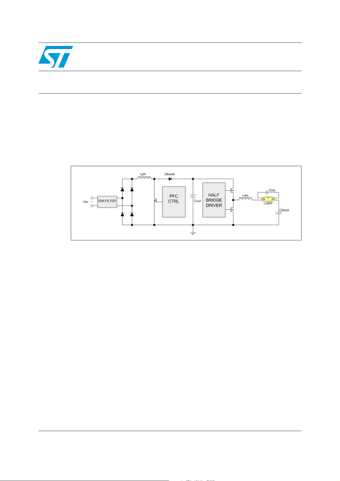
Figure 1. Typical electronic ballast block diagram
March 2009 Rev 1 1/41
www.st.com
Page 2

Contents AN2870
Contents
1 Introduction . . . . . . . . . . . . . . . . . . . . . . . . . . . . . . . . . . . . . . . . . . . . . . . . 4
1.1 Typical configuration . . . . . . . . . . . . . . . . . . . . . . . . . . . . . . . . . . . . . . . . . . 4
1.2 Lamp requirements . . . . . . . . . . . . . . . . . . . . . . . . . . . . . . . . . . . . . . . . . . 4
2 L6585DE combo IC . . . . . . . . . . . . . . . . . . . . . . . . . . . . . . . . . . . . . . . . . . 6
3 Device blocks description . . . . . . . . . . . . . . . . . . . . . . . . . . . . . . . . . . . . 8
3.1 Start-up and shut-down . . . . . . . . . . . . . . . . . . . . . . . . . . . . . . . . . . . . . . . 8
3.2 PFC section . . . . . . . . . . . . . . . . . . . . . . . . . . . . . . . . . . . . . . . . . . . . . . . 10
3.2.1 Error amplifier . . . . . . . . . . . . . . . . . . . . . . . . . . . . . . . . . . . . . . . . . . . . 10
3.2.2 Multiplier block and THD optimizer . . . . . . . . . . . . . . . . . . . . . . . . . . . . 10
3.2.3 Current comparator and choke saturation detection . . . . . . . . . . . . . . . 11
3.2.4 Zero current detection . . . . . . . . . . . . . . . . . . . . . . . . . . . . . . . . . . . . . . 12
3.2.5 Driver . . . . . . . . . . . . . . . . . . . . . . . . . . . . . . . . . . . . . . . . . . . . . . . . . . . 12
3.2.6 PFC protections . . . . . . . . . . . . . . . . . . . . . . . . . . . . . . . . . . . . . . . . . . . 12
3.3 Ballast controller section . . . . . . . . . . . . . . . . . . . . . . . . . . . . . . . . . . . . . 13
3.3.1 Oscillator and timer . . . . . . . . . . . . . . . . . . . . . . . . . . . . . . . . . . . . . . . . 13
3.3.2 Overcurrent control and protections . . . . . . . . . . . . . . . . . . . . . . . . . . . . 14
3.3.3 End of life detection . . . . . . . . . . . . . . . . . . . . . . . . . . . . . . . . . . . . . . . . 16
3.3.4 Shutdown . . . . . . . . . . . . . . . . . . . . . . . . . . . . . . . . . . . . . . . . . . . . . . . . 19
4 Designing with L6585DE . . . . . . . . . . . . . . . . . . . . . . . . . . . . . . . . . . . . . 20
4.1 PFC stage design . . . . . . . . . . . . . . . . . . . . . . . . . . . . . . . . . . . . . . . . . . . 20
4.2 Ballast stage design . . . . . . . . . . . . . . . . . . . . . . . . . . . . . . . . . . . . . . . . . 28
4.3 PCB hints . . . . . . . . . . . . . . . . . . . . . . . . . . . . . . . . . . . . . . . . . . . . . . . . . 39
5 Revision history . . . . . . . . . . . . . . . . . . . . . . . . . . . . . . . . . . . . . . . . . . . 40
2/41
Page 3

AN2870 List of figures
List of figures
Figure 1. Typical electronic ballast block diagram . . . . . . . . . . . . . . . . . . . . . . . . . . . . . . . . . . . . . . . . 1
Figure 2. Block diagram . . . . . . . . . . . . . . . . . . . . . . . . . . . . . . . . . . . . . . . . . . . . . . . . . . . . . . . . . . . . 7
Figure 3. Start-up and shut-down waveforms . . . . . . . . . . . . . . . . . . . . . . . . . . . . . . . . . . . . . . . . . . . 9
Figure 4. PFC section block . . . . . . . . . . . . . . . . . . . . . . . . . . . . . . . . . . . . . . . . . . . . . . . . . . . . . . . . 10
Figure 5. PFCCS pin waveforms . . . . . . . . . . . . . . . . . . . . . . . . . . . . . . . . . . . . . . . . . . . . . . . . . . . . 11
Figure 6. Protections block diagram . . . . . . . . . . . . . . . . . . . . . . . . . . . . . . . . . . . . . . . . . . . . . . . . . 12
Figure 7. Oscillator and starting sequence . . . . . . . . . . . . . . . . . . . . . . . . . . . . . . . . . . . . . . . . . . . . 13
Figure 8. Current control sequence during ignition . . . . . . . . . . . . . . . . . . . . . . . . . . . . . . . . . . . . . . 15
Figure 9. HBCS thresholds summary . . . . . . . . . . . . . . . . . . . . . . . . . . . . . . . . . . . . . . . . . . . . . . . . 15
Figure 10. Window comparator for rectifying effect detection (Cblock to GND). . . . . . . . . . . . . . . . . . 17
Figure 11. Window comparator for rectifying effect detection (lamp to GND) . . . . . . . . . . . . . . . . . . . 19
Figure 12. Typical application . . . . . . . . . . . . . . . . . . . . . . . . . . . . . . . . . . . . . . . . . . . . . . . . . . . . . . . 20
Figure 13. PFC MOSFET losses (example) . . . . . . . . . . . . . . . . . . . . . . . . . . . . . . . . . . . . . . . . . . . . 24
Figure 14. Multiplier characteristics . . . . . . . . . . . . . . . . . . . . . . . . . . . . . . . . . . . . . . . . . . . . . . . . . . . 26
Figure 15. (A) voltage frequency response . . . . . . . . . . . . . . . . . . . . . . . . . . . . . . . . . . . . . . . . . . . . . 30
Figure 15. (B) current frequency response . . . . . . . . . . . . . . . . . . . . . . . . . . . . . . . . . . . . . . . . . . . . . 30
Figure 16. Oscillator characteristic curves . . . . . . . . . . . . . . . . . . . . . . . . . . . . . . . . . . . . . . . . . . . . . . 31
Figure 17. (A) k parameter versus Cosc (pF) . . . . . . . . . . . . . . . . . . . . . . . . . . . . . . . . . . . . . . . . . . . 32
Figure 17. (B) e parameter versus Cosc (pF) . . . . . . . . . . . . . . . . . . . . . . . . . . . . . . . . . . . . . . . . . . . 32
Figure 18. EOL - Cblock to ground . . . . . . . . . . . . . . . . . . . . . . . . . . . . . . . . . . . . . . . . . . . . . . . . . . . 35
Figure 19. EOL - lamp to ground . . . . . . . . . . . . . . . . . . . . . . . . . . . . . . . . . . . . . . . . . . . . . . . . . . . . . 36
Figure 20. Current consumption vs PFC frequency. . . . . . . . . . . . . . . . . . . . . . . . . . . . . . . . . . . . . . . 38
3/41
Page 4

Introduction AN2870
1 Introduction
1.1 Typical configuration
Typical fluorescent lamp electronic ballasts are composed by (Figure 1):
● An input PFC section, if input power is greater than 25 W, usually a TM PFC converter,
that generates a DC output voltage and absorbs power from mains with very high
Power Factor (typically 0.95 or grater) and very low THD (mandatory less than 10%).
● A high frequency half bridge driver, fed by the PFC output, with internal or external
oscillator, a timer and various protections in order to drive correctly the lamp, to avoid to
deliver an excessive power to the lamp and to detect any malfunction of the lamp
(broken lamp, broken cathode or lamp absence)
● An output resonant stage, realized by reactive components (capacitors and inductors),
that, together with the half bridge driver, optimizes the power delivered to the lamp (one
or more) during all working conditions (preheating, ignition and run mode).
1.2 Lamp requirements
Fluorescent lamp, during its normal operation, has to be supplied by means of alternative
and controlled current. In order to reduce the size of the ballast and increase the light
efficiency of the lamp a frequency greater than 20 kHz is typically used. A half bridge quasi
resonant inverter (series-parallel converter Figure 1) is used to obtain sinusoidal current into
the lamp and to reduce the power dissipation of the half bridge switches, in fact zero voltage
switching is achieved.
Lamp current and lamp voltage during normal operation are reported in lamp documentation
and are to be considered as design specification. Moreover, a well preheated lamp ignites at
a lower voltage; this implies a longer lamp life and a greater number of ignitions. The
efficiency of the preheating is mainly related with the total energy delivered to the cathode
(reported on lamp documentation), and then it depends on the time available for this
operation: keeping constant the preheating energy, longer is the preheating time, smaller is
the instantaneous power delivered to the cathode. During the preheating operation the
voltage across the lamp must be kept below a specified value in order to avoid unwanted
ignitions (when these happen, the lamp experiences multiple re-strike and dissipates large
amounts of power).
There are many ways to deliver power to the cathode, but the most used are two:
1. Current controlled preheating: the cathodes are interposed between the choke and the
resonant capacitor so they experience the same current of the resonant LC circuitry. An
efficient preheating is obtained controlling this current and the time of preheating. The
advantages of this method are the cheapness and easiness of design; it has also some
disadvantages, namely the difficulty of keeping low the lamp voltage during preheating
and the fact that during steady state the cathode experiences the sum of the lamp
current and of the resonant capacitor current.
2. Voltage controlled preheating: the current into the cathodes is generated by auxiliary
windings coupled with ballast choke or driven by an auxiliary oscillator. This implies
that, in any case, the design of the preheating circuitry is somewhat independent from
the design of the LC circuitry, even if it requires a lot of external components. This
method is then more efficient, but is cheaper and more difficult to design.
4/41
Page 5

AN2870 Introduction
After a good preheating, the voltage across the lamp is suddenly increased in order to
generate a strike inside the tube and ignite the lamp. This phase should last between 10 ms
and 100 ms.
The strike voltage depends on various parameters, many of which cannot be exactly
evaluated: preheating energy, remaining lamp life, number and efficiency of the past
ignitions. An insufficient preheating causes greater ignition voltage and a subsequent stress
of the cathodes that lose small amounts of material that darken the region of the tube near
to the cathode itself (sputtering).
Lamp ageing is related with the symmetrical or, more often, asymmetrical increasing of the
cathodes resistance. A symmetrically aged lamp absorbs more power causing hard
switching and over-current. Asymmetrically aged lamps experience a current that is more
intense in one direction than in the other. This implies that the current flowing into the lamp
has positive or negative mean value (DC component). This effect can be detected
measuring the mean values of the lamp voltage that should be zero in normal lamps. The
worst case of rectifying effect causes the current flowing only in one direction: the voltage
across the resonant capacitor can reach very high values and heavy hard switching is
detected.
When symmetrical or asymmetrical ageing of the lamp reaches a value indicated in
international norms, the lamp reaches its end of life (EOL).
5/41
Page 6

L6585DE combo IC AN2870
2 L6585DE combo IC
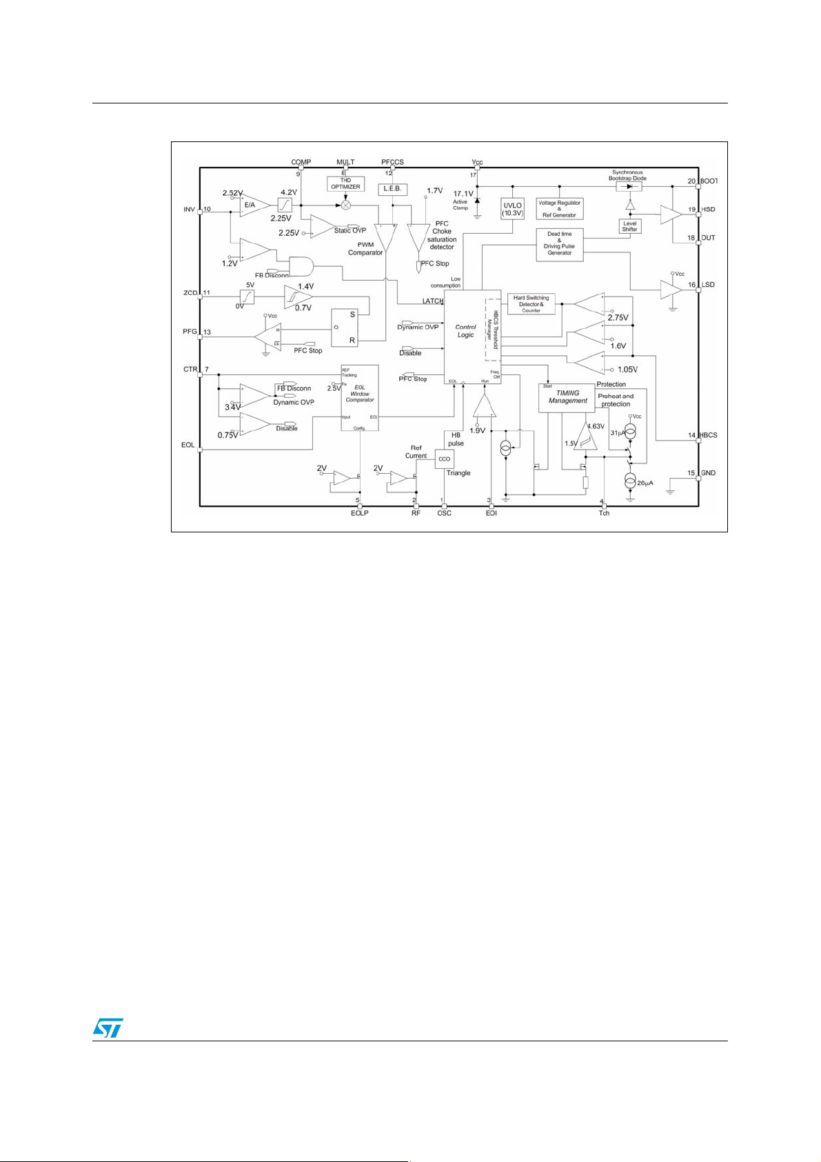
The L6585DE embeds both a PFC converter and a ballast regulator in a single SO20
package. It is intended to design complete high power electronic ballasts with a single chip.
● The most significant features of the L6585DE concern the following points:
● Transition mode PFC converter with over voltage and over current protection.
● Half-bridge controller with High voltage driver (600 Vdc) and integrated bootstrap
diode.
● 3% precise, fully programmable oscillator.
● Flexibility in programming preheating time and ignition time.
● Configurable EOL detection and over current protection.
● Hard switching detection.
The PFC section achieves current mode control operating in Transition Mode. The multiplier,
together with the internal THD optimizer, reduces input current distortion, and allows
reaching very high performances also in wide-range-mains operation and large load range.
The PFC output voltage is controlled by means of a voltage-mode error amplifier and a
precise internal voltage reference.
A static and dynamic OVP protects the IC from excessive output voltage and an over current
protection turns off the PFC gate driver in case of PFC choke saturation.
The PFC driver is able to provide 300 mA (source) and 600 mA (sink).
The half bridge section is driven by a current controlled oscillator (CCO) and the internal
control logic.
The steady state frequency, the preheating frequency, the pre-heating time, the over-current
protection time and the ignition time are independently set by means of six external
components (resistors and capacitors).
An over-current protection limits the voltage across the HBCS pin acting directly on the CCO
realizing a precise closed loop control. This control lasts for a time set by the Tch pin and,
after that, if the fault condition is still present, the IC is stopped in low consumption mode.
The HBCS voltage amplitude depends on actual operating mode, then this protection can
detect either a broken lamp during ignition (in this case the current regulation implies the
lamp voltage regulation) or the symmetrical ageing of the lamp during run mode.
An internal window comparator can be simply configured setting the window amplitude or
the comparator reference in order to detect the EOL status. The programmability of
comparator reference makes the L6585DE compliant with either “lamp-to-ground” (fixed
reference) or “block capacitor-to ground” (tracking with CTR) configurations.
The drivers of the half-bridge provide 290 mA source and 480 mA sink.
6/41
Page 7
AN2870 L6585DE combo IC
Figure 2. Block diagram
7/41
Page 8

Device blocks description AN2870
3 Device blocks description
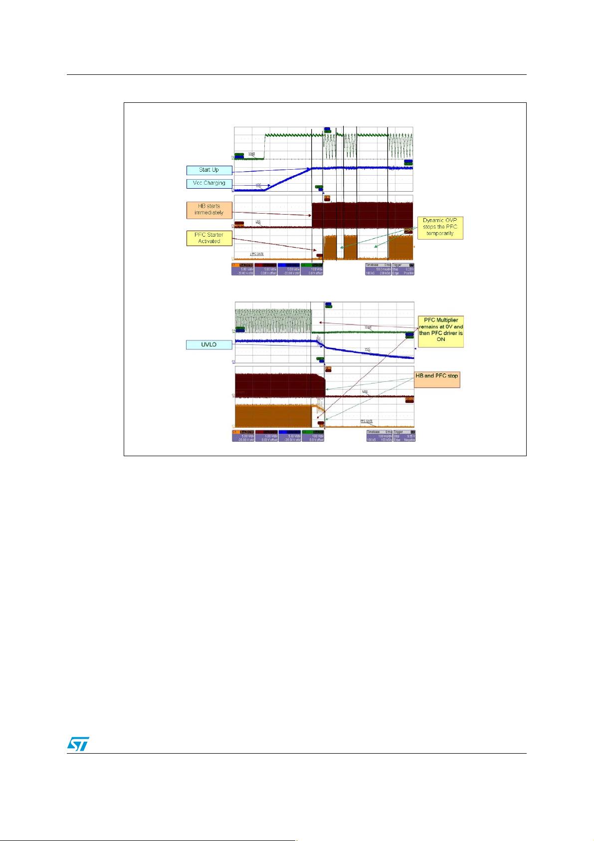
3.1 Start-up and shut-down
During start-up the chip is supplied through a resistive path from the rectified AC Mains
voltage whereas, during normal operation, a self-supply source is recommended: a charge
pump, an auxiliary winding coupled either with PFC choke or resonant choke, or an auxiliary
converter.
As the voltage at Vcc pin reaches the turn-on threshold (Vcc
, Figure 3-A), the chip is
ON
enabled and (unless a lamp absence is detected) the Half-Bridge and the PFC sections
start at the same time (independently):
● The PFC section, as the synchronization signal at pin ZCD is not yet generated by the
external ZCD circuit, is forced to switch by internal starter (f
= 6 kHz (typ)) for the
starter
first few switching cycles, until the control loop operates correctly at a frequency higher
than f
● The oscillator starts switching at a preheating frequency set by values of C
and R
At shut-down (Figure 3-B), when the V
starter
PRE
.
, R
OSC
RUN
.
decreases below the UVLO threshold (either in
CC
case of mains removal or in case of fault):
● All drivers are off;
● EOI pin is discharged (the internal switch is on);
● RF reference is disabled;
● Tch is discharged.
8/41
Page 9
AN2870 Device blocks description
Figure 3. Start-up and shut-down waveforms
A) Start-up
B) Shut down
9/41
Page 10
Device blocks description AN2870
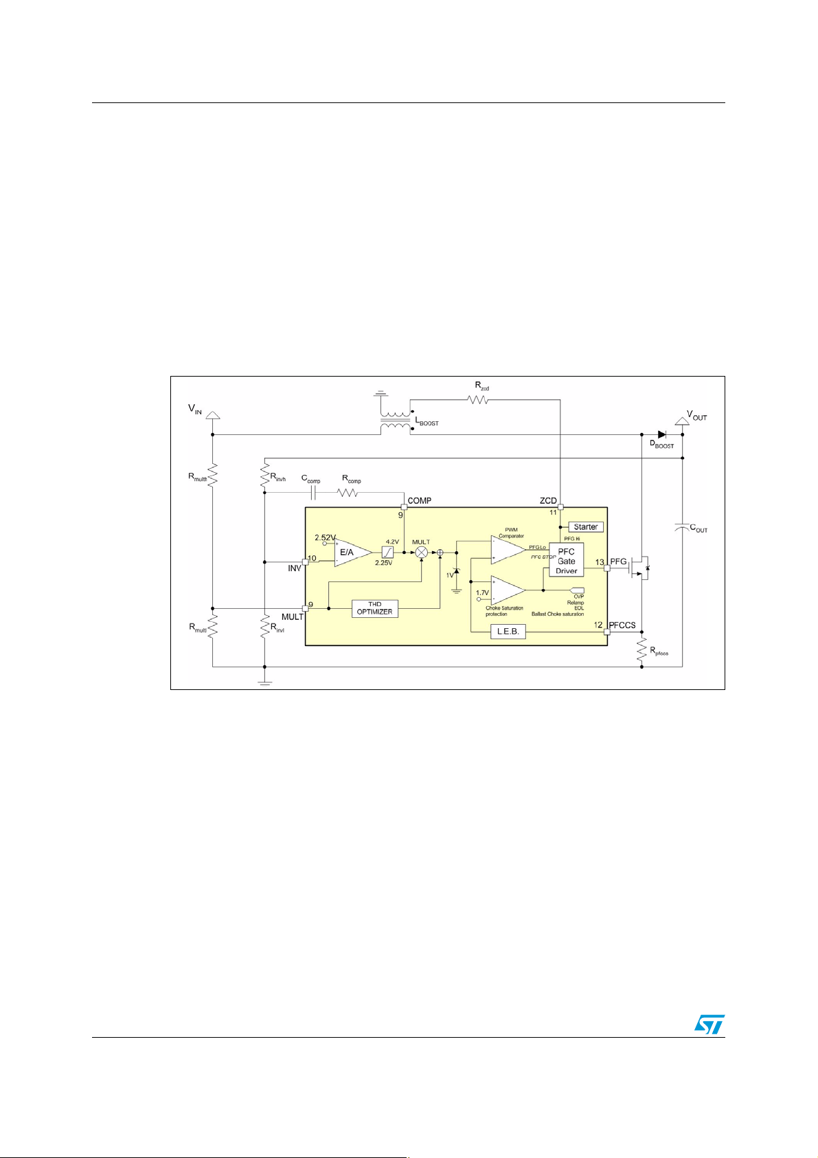
3.2 PFC section
3.2.1 Error amplifier
The error amplifier (E/A, Figure 4) is used to close the output voltage control loop. Its non
inverting input is connected to a precise voltage reference (2.52 V), the inverting input and
the output are externally available (pin 10 –INV; pin 9 – COMP).
The compensation network, placed between pins INV and COMP, is needed to reject the
mains ripple.
The E/A output dynamic is internally clamped: it can swing between 2.25 V and 4.2 V in
order to speed up the recovery after the E/A saturates low due to an over-voltage (static
OVP) or saturates high because of an over-current.
Figure 4. PFC section block
3.2.2 Multiplier block and THD optimizer
The multiplier (Figure 4) gives the sinusoidal voltage reference to the current sense in order
to absorb from the mains a sinusoidal current. This current will be function of both input
voltage and load current then this block has two inputs: the first one (Pin MULT – 8) takes a
partition of the instantaneous rectified line voltage and the second one (Pin COMP – 9) is
the output of the E/A.
An internal voltage clamp (1 V) sets the maximum allowed voltage of the multiplier output,
then it act as PFC current limiter.
When the rectified input voltage reaches 0 V the boost inductor cannot store enough energy
to discharge the input capacitor: this event increases the THD. In order to avoid this
additional distortion, a THD optimizer block is placed between the output of the multiplier
and the current sense comparator.
The characteristic curves of the multiplier block are reported in Figure 14.
10/41
Page 11
AN2870 Device blocks description
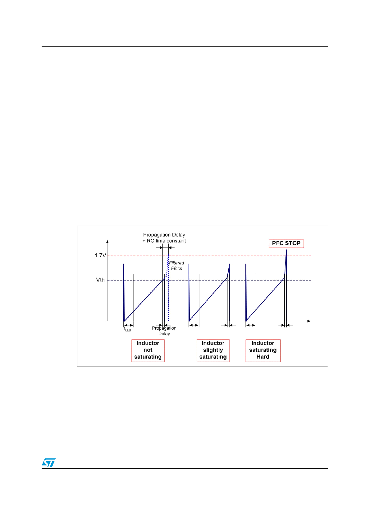
3.2.3 Current comparator and choke saturation detection
The current comparator senses the voltage across the current sense resistor (R
pfccs
) and,
by comparing it with the programming signal delivered by the multiplier, determines the
exact time when the external MOSFET has to be switched off.
When PFC MOSFET is turned on, parasitic drain capacitances are discharged and an
intense current spike can be seen by PFCCS (Figure 5). In past solutions, an RC filter
between sense resistor and current sense input was commonly used to reject these spikes,
but it introduced a delay between the instant the current crosses the threshold and the
actual activation of internal comparator. This delay may cause the inductor saturation, then
an over dimensioned inductor had to be used. In L6585DE, an internal leading edge
blanking structure (LEB) masks the first 200 ns of the PFC gate at the time current spikes
occurs; the filter is no longer necessary and the inductor can be smaller and lighter. On the
other hand this LEB limits the maximum available “ON time”.
Moreover, the device is provided with a second comparator on the PFC current sense pin
that turns off immediately the PFC MOSFET if the voltage on the pin, normally limited within
1.0 V, exceeds 1.7 V. A current peak limiting control is therefore achieved avoiding MOSFET
overheating in case of boost inductor’s hard saturation. In this case the current up-slope
becomes so large (50-100 times steeper) that during the current sense propagation delay
the current may reach abnormally high values.
Figure 5. PFCCS pin waveforms
11/41
Page 12

Device blocks description AN2870
3.2.4 Zero current detection
The zero current detection (ZCD) block switches on the external PFC MOSFET as the
current through the boost inductor has gone to zero. This feature allows TM operation.
When the circuit is running, the signal for ZCD is obtained with an auxiliary winding coupled
with the boost inductor. A Schmidt trigger prevents false activations and an internal clamp
limits the voltage across the pin during normal operation in 0 V-5 V range. As at start-up no
signal is coming from the ZCD, an internal starter is needed in order to turn on the external
MOSFET and to arm the ZCD trigger.
The repetition rate of the starter is ≅ 6 kHz and this maximum frequency must be taken into
account at design time.
3.2.5 Driver
A totem pole buffer, with 300 mA source and 600 mA sink capability, allows driving an
external MOSFET. A pull-down circuit holds the output low when the device is in UVLO
conditions, to ensure that the external MOSFET cannot be turned on accidentally.
3.2.6 PFC protections
The device is provided with a double over-voltage protection (OVP).
The first over voltage protection, also called dynamic OVP, is activated immediately when
CTR pin (pin 7) goes above 3.4 V. The maximum voltage allowed for the output voltage
(V
) is defined by a resistive divider connected between output voltage and CTR pin.
OVP
In case of over voltage, the output of the E/A will tend to saturate low with a long constant
time, because of the bandwidth of this stage (typ. 10 Hz).
If the over-voltage lasts so long that the output of E/A goes below 2.25 V, the PF gate driver
is stopped and Tch timer is started. If E/A output voltage doesn’t return above 2.25 V after
the timer finishes its count, the IC is stopped in latch condition. This protection prevents
damages due to the connection to an excessive input voltage.
An intense high voltage (e.g. a surge) may break the upper resistors (one or more than one)
of the voltage dividers connected to input voltage (MULT biasing) or to output voltage (INV
and CTR biasing). Losing of the bias on pin INV implies losing of the control of the loop: in
fact E/A output saturates high and causes an increased output voltage, eventually not seen
by OVP because of failure on CTR voltage divider. The feedback disconnection protection
prevents this failure stopping the PF gate if INV voltage falls below 1.2 V and CTR pin goes
above 3.4 V. CTR pin can be also used to disable the IC pulling its voltage below 0.8 V.
Figure 6. Protections block diagram
12/41
Page 13
AN2870 Device blocks description
3.3 Ballast controller section
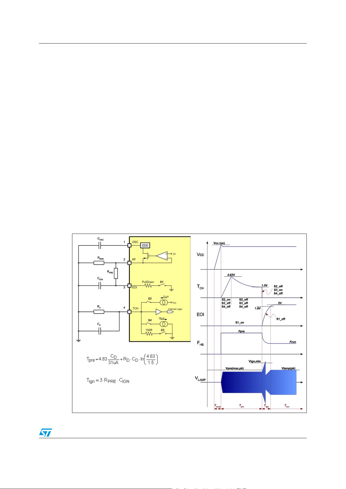
3.3.1 Oscillator and timer
The half bridge driver oscillation is regulated by a current controlled oscillator (CCO): it
needs a capacitor connected to OSC pin (pin 1) and uses the current flowing outside RF pin
(pin 2) as reference.
The RF pin has a 2 V precise voltage reference that let the designer fix the run mode
frequency simply connecting a resistor between RF pin and GND (Rrun).
The EOI pin (pin 3) is driven by the internal logic in order to set the frequency during the
preheating and to control the lamp current during an over-current event in the half bridge.
Preheating frequency is set by the parallel of Rrun and a resistor (Rpre) placed between RF
and EOI: in fact during the preheating the EOI pin is pulled to GND.
TCH pin is connected to the parallel of a resistor (R
) and a capacitor (CD) and is used in
D
order to define the preheating time and the protection time; its cycle (Tch cycle) is
composed by the following steps:
1. A 31 μA current generator charges the C
2. When TCH voltage reaches 4.63 V, the TCH pin is left in high impedance status and C
is discharged by R
,
D
causing TCH voltage to rise linearly,
D
D
3. When TCH voltage reaches 1.5 V the cycle finishes and an internal resistor pulls down
the TCH pin to GND.
Figure 7. Oscillator and starting sequence
13/41
Page 14

Device blocks description AN2870
3.3.2 Overcurrent control and protections
Limiting the current flowing into the half bridge:
● The lamp voltage during the ignition phase is limited
● The power of the lamp during run mode is limited
Ignition phase: (see Figure 8) if the VHBCS high threshold (HBCSH = 1.6 V) is crossed
(because the lamp doesn’t ignite), the following actions are taken by L6585DE:
1. A current, whose amplitude is proportional to the time the V
sunk from EOI and consequently from RF pin. This results in a frequency increase that
reduces the resonant network current and therefore the lamp voltage.
2. A reduced time is calculated by Tch pin:
a) The 31µA generator charges C
b) Instead of leaving C
quickly C
to 1.5 V (S4 on)
D
to be discharged by RD, a 26 µA current generator discharge
D
to 4.63 V
D
c) The pull down switch S3 completes the reduced cycle
is above threshold, is
HBCS
The reduced Tch cycle depends only on C
value and is equal to:
D
Equation 1
⎛
63.4
⎜
CT ⋅≅
Dreduced,Tch
⎜
I
⎝
+=
I
⎞
5.163.4
−
⎟
⎟
snk,Tchsource,Tch
⎠
C269740
D
At the end of the Tch cycle, during the first subsequent low side on time, the HBCS voltage
is checked: if V
is higher than a threshold (HBCS
HBCS
) the IC is stopped in latched
H,test
condition, otherwise EOI pin is released in high impedance status. When EOI voltage
reaches 1.9 V the IC enters the run mode.
The sense resistor value defines the maximum current that can flow during ignition and then
the maximum allowed lamp voltage.
The linear growth of the lamp voltage, thanks to the exponential decrease of the operating
frequency during ignition allows a better control of the voltage thanks to a lower dV/dF
In case of choke saturation the intense current results in very high V
HBCS
. The 2.75
sw
.
threshold triggers this event and stops immediately the IC.
Run mode: During this phase, current control similar to the one present during ignition is
available in case of an over-current due to symmetrical ageing of the lamp. It follows the
same rules, but the threshold is equal to 1.05 V instead of 1.6 V.
Also during run mode the saturation protection is active: in case of choke saturation due to
lamp breaking, lamp removal and capacitive mode where V
experiences a spike whose
HBCS
amplitude is higher than 1.6 V and whose duration is longer than 300 ns. This kind of event
causes the IC turn-off in latched condition.
The lamp ageing causes the shift of peak of the resonance curve towards the run frequency.
This results in hard switching behavior: the half bridge doesn’t work at ZVS and spikes
appears at HBCS pin. These spikes have very high amplitude (up to 8 V) and short duration
(30 ns-50 ns).
14/41
Page 15
AN2870 Device blocks description
During hard switching the power dissipation of half bridge MOSFETs increases rapidly.
L6585DE detects these pulses and shuts down the half bridge after 350 (typ) subsequent
pulses.
The hard switching detection structure is masked during preheating and ignition: in fact
during this phase the frequency changes cause hard switching that is unavoidable but is not
dangerous.
In
Figure 9 a summary of the protection thresholds is reported:
Figure 8. Current control sequence during ignition
Figure 9. HBCS thresholds summary
15/41
Page 16

Device blocks description AN2870
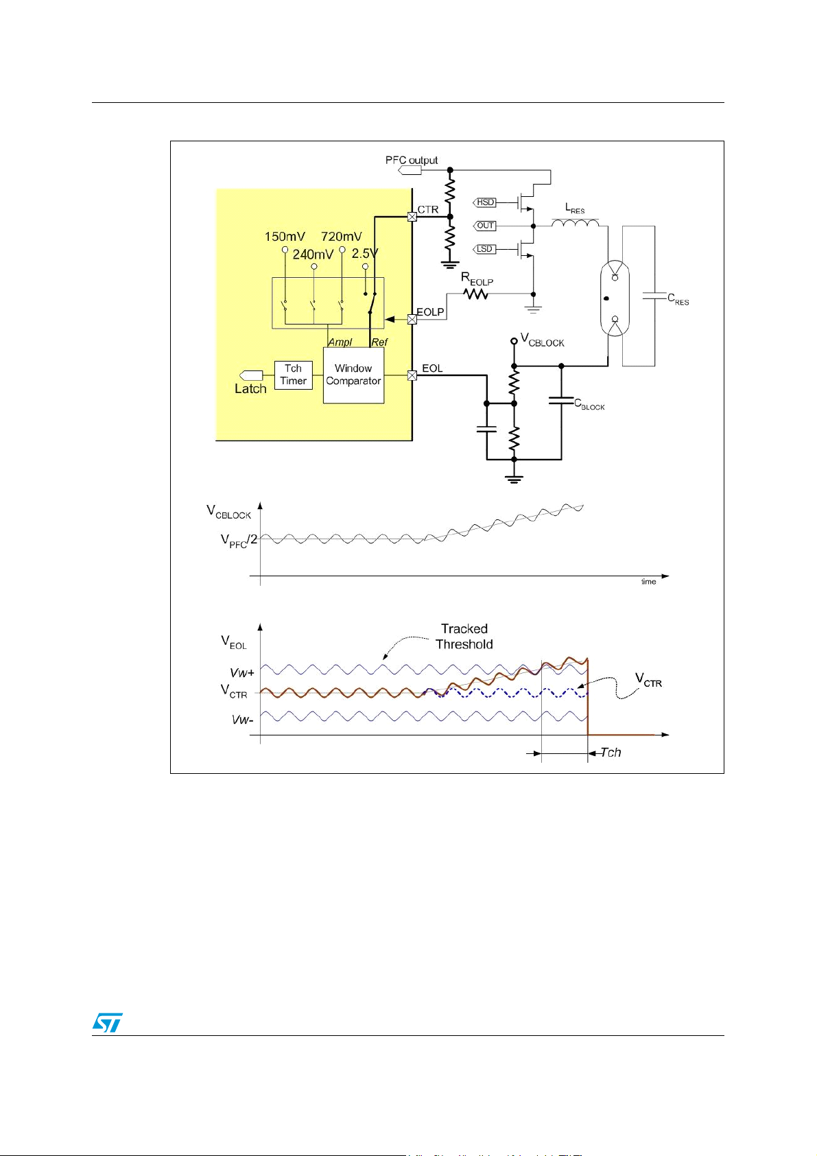
3.3.3 End of life detection
When the lamp becomes older and approaches its end of life, its equivalent resistance
increases symmetrically or asymmetrically.
In symmetrical ageing a modification of the frequency response of the resonance network
can be seen and, consequently, an increasing of lamp current and the appearance of hard
switching events: in fact the resonance frequency is now closer to operating frequency.
In asymmetrical ageing the current flowing in one direction is greater than the current
flowing in the other; this means that lamp voltage and current waveforms have no longer
zero mean value.
lamp voltage that can be either positive or negative. The reference and the amplitude of this
comparator can be set choosing the value of a resistor connected between EOLP pin and
GND accordingly with the following table.
Table 1. Comparator amplitude
EOLP resistor Symbol Reference Half–window amplitude
R
EOLP > 620 kΩ RFH Fixed 2.5 V ± 720 mV
A window comparator measures the variation of the DC component of the
220 kΩ < R
75 kΩ < R
22 kΩ < R
EOLP < 270 kΩ RTL Tracking with CTR - 240 mV / + 250 mV
EOLP < 91 kΩ RFL Fixed 2.5 V ± 240 mV
EOLP < 27 kΩ RTL Tracking with CTR - 150 mV / + 160 mV
This comparator can be used in both the two most used ballast configurations: Blocking
capacitor to ground and lamp to ground.
Block capacitor to ground (Figure 10): During normal operation the DC mean value
across Cblock is equal to the half of the output voltage of the PFC. A resistive divider is
placed across the block capacitor to sense its DC voltage: the asymmetric effect appears as
a shifting of this DC value.
Any voltage ripple or disturbance across the output voltage is present also on Blocking
Capacitor and may alter the correct detection of a lamp at the end of its life.
In order to reject all this disturbances, the reference of the window comparator is connected
to CTR pin (Tracking reference configurations): in fact this pin is connected directly to the
output voltage and experiences the same ripple voltage. The rejection of the PFC output
voltage low frequency ripple allows using a smaller bulk capacitance.
16/41
Page 17
AN2870 Device blocks description
Figure 10. Window comparator for rectifying effect detection (Cblock to GND)
17/41
Page 18

Device blocks description AN2870
Lamp to ground (Figure 11): the resistive divider senses the voltage across the lamp. As
the L6585DE doesn’t have a negative rail, it is necessary to shift the external signal; this can
be done (for example) using two Zener diodes connected back-to-back between the EOL
pin and the centre of the resistive divider.
The Zener voltages should differ by an amount as close as possible to the double of the
internal reference to have a symmetrical detection, in fact:
Let be V
Voltage divided by the divider factor K
Zener and V
● V
●
UP
V
DOWN
and V
UP
the forward voltage of the Zener (@ 5.5 μA)
F
= V
LAMP,MAX/KD
= V
LAMP,MIN/KD
the maximum allowed values of the DC component of the Lamp
DOWN
= V
REF
= V
, W the window amplitude, VZ the Zener voltage of a
D
+ W/2 + V
– W/2 – VZ2 – V
REF
Z1
+ V
F
F
It must be:
● V
UP
= - V
DOWN
therefore:
● 2 V
= VZ2 − V
REF
Z1
The biasing current available at pin EOL is equal to 5.5 μA then the VZ1 Voltage should be
greater than 8 V in order to have a more precise EOL threshold.
In this case the window comparator can be referenced to the 2.5 V internal reference as
external disturbances don’t influence the lamp voltage mean value (Fixed reference
configurations).
In the
Figure 11 is shown the case of asymmetric rectification with positive shifting.
To avoid an immediate intervention of the EOL protection, a filtering is introduced: as soon
as the voltage at pin EOL goes outside the window of the comparator a Tch cycle is started.
The IC is stopped if, at the end of the Tch cycle, the EOL voltage is again outside the limits.
18/41
Page 19

AN2870 Device blocks description
Figure 11. Window comparator for rectifying effect detection (lamp to GND)
3.3.4 Shutdown
A second comparator, with a threshold equal to 0.8 V, has been introduced on the pin CTR
in order to stop the IC if the CTR pin is pulled to ground. If IC is not in latched condition
when CTR is pulled down, a new starting sequence is performed as CTR pin voltage is
higher than the threshold; this behavior can be used for shutdown.
19/41
Page 20

Designing with L6585DE AN2870
4 Designing with L6585DE
Figure 12. Typical application
4.1 PFC stage design
Output voltage and dynamic OVP
Output voltage is set designing a voltage divider connected to INV pin:
Equation 2
The maximum output voltage is set designing a voltage divider connected to CTR pin:
Equation 3
Both R
series in order to increase the reliability of the application against over-voltages.
INV,Hi
and R
should be composed by a suitable number of resistors placed in
CTR,Lo
OUT
⎛
R
⎜
1V52.2V
+⋅=
⎜
R
⎝
⎛
⎜
1V4.3V
MAX,OUT
+⋅=
⎜
⎝
⎞
Hi,INV
⎟
⎟
Lo,INV
⎠
R
R
⎞
Hi,CTR
⎟
⎟
Lo,CTR
⎠
20/41
Page 21

AN2870 Designing with L6585DE
(
Boost choke design
PFC stage operates in transition mode; for a certain value of input voltage the on time (Ton)
is constant over the entire half period of the input voltage.
The frequency changes along the period of the input voltage: in particular the frequency is
the lowest when the input voltage reaches its maximum.
Moreover the frequency is higher if the output power is low and the frequency variation
changes if input voltage changes.
The internal starter requires a minimum PFC frequency equal to around15 kHz.
Equation 4
f
PFC
f
2
⎛
V
in
⎜
1
=
in
=
min,PFC
−⋅
⎜
LP2
⋅⋅
⎝
2
⎛
V
in
⎜
1
⎜
LP2
⋅⋅
in
⎝
V2
⋅
−⋅
in
V
out
mainsin
V
out
⎞
⎟
kHz15
≥
⎟
⎠
⎞
)
tf2sinV2
⋅⋅π⋅⋅
⎟
⎟
⎠
Using Eq.4 with both minimum and maximum value of Vin, the value of L can be selected as
the minimum obtained value. Even the maximum frequency should be checked to avoid to
absorb too much current from Vcc and to degrade the input performances due to excessive
frequency (> 450 kHz) in correspondence to zero input voltage.
The calculation of the maximum frequency is only a rough evaluation of the real frequency;
in fact the presence of the THD optimizer reduces the frequency near the crossover of the
input voltage.
The maximum current flowing into the choke can be evaluated as twice the maximum input
current:
Equation 5
P
in
max,L
22I ⋅⋅=
V
min,in
The ohmic power losses will be evaluated considering the RMS value of the current:
Equation 6
P
2
I =
RMS,L
in
V
3
min,in
The choke is realized around of a gapped ferrite core; the core shape has to be selected
considering the electrical parameters (Eq.4,5 and 6), the dimensions of the ballast and the
availability of the selected core. The core should be made by a material suitable for high
frequency operation.
21/41
Page 22

Designing with L6585DE AN2870
(
)
The number of turns and the length of the gap can be calculated as follows (L in uH, Bmax
in tesla, Ae in square millimeters and μ
=4π*10-7):
0
Equation 7
N
=
A
L
⎪
AB
⎪
emax
⎬
L
⎪
2
⎪
N
⎭
gap
2l
2
μ
AN
e
0
×=→
L
LI
⎫
max
=
Wire section is selected in order to fit the winding window of the coil former (preferred if
slotted).
In order to evaluate the actual copper losses the DC resistance of the winding must be
multiplied by a factor that depends on skin effect. Using a wire composed by multiple
conductors reduces this factor.
The copper losses can be evaluated as:
Equation 8
2
RIP ⋅=
RMS,L,L
Ω
HF,wire
Ferrite losses can be checked on ferrite manufacturer catalogs.
ZCD auxiliary winding must be able to develop the triggering pulse for ZCD pin
= 1.4 V). The voltage across the auxiliary winding will be:
(V
arm
Equation 9
V4.1mV2VV
⋅>⋅−=
inoutzcd,aux
The current flowing in ZCD pin must be limited by means of a resistor connected between
auxiliary winding and ZCD pin. Although the maximum ZCD pin current is around 5 mA, a
smaller value should be chosen in order to limit power dissipation and increase the
application reliability.
Equation 10
V2
⋅
R
=
ZCD
max,in
Im
⋅
ZCD
22/41
Page 23

AN2870 Designing with L6585DE
MOSFET selection
PFC MOSFET is to be selected considering the maximum current flowing into the switch,
the maximum voltage between drain and source and the maximum allowed losses.
Maximum allowed losses depend on maximum allowed junction temperature; an ambient
temperature equal to 70 °C – 80 °C is usually considered.
Power losses can be summarized as follows:
● Conduction losses: due to ohmic resistance of the MOSFET channel during its on
state; these losses are prevalent at minimum input voltage.
● Switching losses: experienced only during turn off transitions.
● Capacitive losses: experienced only during turn on transitions when the MOSFET has
to discharge the parasitic capacitance present at its drain. These losses are very high
at higher input voltages.
Conduction losses are related to R
and RMS value of the drain current:
DS(on)
Equation 11
2
⎛
2
RMS,MOS
P
⎜
=
8I
⎜
V
⎝
⎡
⎞
1
in
⎟
−
⎢
⎟
6
⎢
rms,in
⎠
⎣
Considering a maximum conduction losses less than P
24
9
π
COND,max
⎤
V
rms,in
⎥
V
⎥
OUT
⎦
, the maximum R
DS(on)
,
measured at 100 °C, can be found as follows:
Equation 12
P
(max)R <
ON,DS
max,COND
2
I
RMS,MOS
Switching losses are directly related to frequency, to output voltage, to input current and fall
time of drain of the MOSFET. The frequency should be averaged over the half period of the
mains and the fall time of the MOSFET can be found on MOSFET datasheet.
Equation 13
2
f
SW
V
=
⎛
RMS,in
⎜
−
1
⎜
⋅⋅
LP2
in
⎝
V
22
⋅
π
V
RMS,IN
OUT
⎞
⎟
⎟
⎠
Equation 14
P
VftIVftP ==
OUTswfrms,inOUTswfcross
in
V
rms,in
Capacitive losses are present only if instantaneous input voltage is greater than half the
output voltage. In fact when the inductor current becomes zero the parasitic capacitances
seen at the drain node starts to resonate with parasitic inductances causing a damped
oscillation whose peak to peak amplitude is equal to V
When V
in<VOUT
/2 the drain voltage at MOSFET turn on is almost zero.
OUT
- Vin.
23/41
Page 24

Designing with L6585DE AN2870
[
The time when input voltage is greater than V
/2 can be calculated as follows:
OUT
Equation 15
⎛
V
OUT
⎜
arcsin
⎜
1
f2
mains
⎝
=
t
1
t
2
⋅⋅
V22
π
f2
mains
−=
t
1
Within t2-t1 interval capacitive losses can be written as:
Equation 16
⎛
⎜
⎜
⎝
3
1
2
VC3.3fP
Drainossswcap
()
2
Where
Equation 17
t
2
∫
t
1
⎞
⎟
⎟
rms,in
⎠
()
⎞
2
+++=
VCCC
2
]
−ω⋅=
outrms,inmainsrms,Drain
⎟
Drainextossrss
⎟
⎠
dtVtsinV22f2V
These losses are greater at higher input voltage.
Figure 13 illustrates an example of calculation in wide range application
(Pin = 64 W, MOSFET STx7NM50).
Figure 13. PFC MOSFET losses (example)
24/41
Page 25

AN2870 Designing with L6585DE
Boost diode selection
Boost diode experiences a maximum current equal to maximum boost inductor current, an
average current equal to P
Equation 18
OUT/VOUT
and a RMS current equal to:
22
2
2
III
rms,Lrms,d
RMS,MOS
4
=−=
π
3
The maximum reverse voltage must be greater or equal to V
P
in
VV
rms,inOUT
and a fast Schottky diode is
OUT
suggested.
Diode power losses can be calculated using the formula reported in diode datasheet:
Equation 19
2
IKIK ⋅+⋅
rms,d2AV,d1
Bulk capacitor selection
Output voltage ripple is due to capacitance value and equivalent series resistor (ESR) of
bulk capacitor. ESR value is a function of frequency: higher the frequency, lower the ESR
value. The worst ESR will be measured in correspondence of the peak of the input voltage,
when the PFC frequency reaches the minimum frequency.
Equation 20
P
V ⋅+
=Δ
OUT
OUT
Rms value of the bulk capacitor current is:
CVf4
⋅⋅⋅π
outOUTmains
IESR
RMS,Cf@
outmin,PFC
Equation 21
2
⋅
I
OUT ⎟
=
RMS,C
232
π
9
P
⋅
in
⋅
VV
⎛
⎜
−
⎜
OUTrms,in
⎝
P
V
OUT
OUT
2
⎞
⎟
⎠
Multiplier biasing and PFC current sense resistor selection
The multiplier biasing proceeds as follows (Figure 14):
1. Calculate the range of the peak of the input voltage.
2. Consider the characteristic curve that exploits the maximum slope and the point that
guarantees, on this curve, a linear behavior. Indicate this point as (V
mult,1,VCS,1
)
25/41
Page 26

Designing with L6585DE AN2870
Figure 14. Multiplier characteristics
3. At minimum input voltage, Vmult had to be biased to V
by means of a voltage
mult,1
divider connected between the rectified input mains and ground. The divider factor is:
Equation 22
V
kp
1,mult
V
min,in
pk
4. PFC sense resistor is chosen in order to obtain V
R
==
lo,mult
RR
+
hi,multlo,mult
at maximum input current (i.e. at
CS,1
minimum input voltage):
Equation 23
R
PFCCS
V
1,CS
==
I
max,L
VV
⋅
min,in1,CS
P22
⋅⋅
in
5. Check Vmult when Vin assumes its maximum value: this new bias point should lie on
the linear segment of a characteristic curve.
The upper resistor value should be obtained using a suitable number of resistors in series in
order to increase the reliability of the application. Furthermore a capacitor placed in parallel
with lower resistor helps filtering the high frequency components of the signal; the cut
frequency of this filter can be placed at ten times the mains frequency, i.e. at 500 Hz.
Error amplifier compensation
Error amplifier compensation design proceeds as follows:
Direct gain of the PFC control loop can be written as (cfr AN966):
Equation 24
1
=
)s(G
26/41
V
4
2
Vkk
out
R
rms,inpM
R
PFCCS
out
1
CR
+
s1
outout
2
Page 27

AN2870 Designing with L6585DE
Where R
is the effective resistance of the load (i.e. V
out
(reported in datasheet) and C
is the bulk capacitor.
out
OUT
2
/P
), kM is the multiplier gain
OUT
In order to compensate the loop and reject the ripple superimposed to the output voltage,
the loop gain at 100 Hz should be less than -60 dB. The transfer function of the error
amplifier, compensated with a simple capacitor can be written as:
Equation 25
comp
()
sG =
1
RsC
invhcomp
and:
Equation 26
⎞
⎟
⎟
CR
⎟
outout
⎟
2
⎠
π=
001.0
=
Hz1002s
() () ()
comploop
=⋅=
sGsGsG
Using a high value for
⎛
⎜
⎜
⎝
R
the value of C
invh
⎛
⎜
⎞
1
RsC
invhcomp
1
⎟
⎜
⋅
⎟
⎜
4
⎠
⎜
⎝
comp
2
Vkk
rms,inpM
V
out
is reduced.
R
R
out
pfccs
1
s1
+
Input rectifier
This component is needed to supply the PFC stage with a rectified voltage.
The reverse voltage should be greater than twice V
, the forward current greater than
in,max
maximum input current and the power dissipation greater than:
Equation 27
P ==
4
2
F(max)rms,inB
P
in
22VI
V
V
F
(min)rms,in
Input capacitor
At this stage of design the current absorption is impulsive. The mean value of this current is
in phase with the input voltage, but the high frequency components have amplitude equal to
twice the amplitude of the mean value, therefore can create interferences with nearby
electronic equipment. An input filter capacitor must be placed between the rectifier and the
PFC stage in order to reduce the high frequency current ripple superimposed to the input
current.
Let be
current:
Equation 28
r the maximum allowed ratio between ripple amplitude and mean value of the input
I
sw
min
RMS,in
Vfr2
⋅⋅⋅π
=
(min)RMS,in
C
=
min,in
min
P
in
Vfr2
⋅⋅⋅π
2
(min)RMS,insw
27/41
Page 28

Designing with L6585DE AN2870
The mean value of the PFC frequency is calculated accordingly with Eq.13.
This capacitor may worsen the overall performance of the PFC stage: in fact the energy
stored in it may not be transferred to inductor when the input voltage is near zero. This is the
main reason of the introduction of the THD optimizer.
Other input circuitry
The EMI behavior of the circuit needs to be improved with a suitable EMI filter, a fuse with
inrush limiter can be introduced for improved reliability against burst and surge events and
finally also a surge suppressor (varistor) can be needed.
4.2 Ballast stage design
Resonant network and operating point design
The values of resonant inductor and resonant capacitor and the operating frequencies are
chosen in order to:
a) Supply the lamp with correct voltage and current during run mode
b) Maintain lamp voltage lower than Vpre during preheating mode
c) Develop a suitable high voltage across the lamp during the ignition
The resonant network when the lamp is off has a very high Q factor and the resonant
frequency is very close to the ideal resonant frequency of an LC resonator.
The relationship between lamp voltage and frequency can be easily found using the Fourier
transform and considering the fundamental harmonic of the square wave generated by the
half bridge.
Input voltage will be:
Equation 29
2
V
V
=
outpk,bal
π
Useful parameters are resonant frequency f0, characteristic impedance Z0 and Q factor:
Equation 30
⎧
f
=
0
⎪
⎪
⎪
⎪
Z
⎨
0
⎪
⎪
⎪
Q
⎪
⎩
1
CL2
π
=
R
lamp
Z
resres
L
res
C
res
V
run
==
ZI
0
0run
Where V
run
and I
are respectively the lamp voltage and lamp current.
run
The suitable frequencies to obtain the desired operating parameters can be calculated as
follows:
28/41
Page 29

AN2870 Designing with L6585DE
Equation 31
2
1
⎛
2
⎜
⎝
ff
=
0run
⎞
−
⎟
Q
⎠
⎡
V2
f
⎢
f
=
pre
2
0ign
out0
⎢
⎢
⎣
1ff
+=
+
IZ
⋅⋅π
pre0
V2
out
⋅⋅π
V2
ign
1
⎛
2
⎜
⎝
⎛
⎜
⎜
⎝
⎞
−+
⎟
22
Q
⎠
V2
out
IZ
⋅⋅π
⎛
⎜
4
+−
⎜
⎝
2
2
⎞
⎟
+
⎟
pre0
⎠
V4
out
⋅⋅⋅π
⎤
⎥
⎥
⎥
⎦
2
⎞
⎟
⎟
I2QZ
run0
⎠
V2
out
1f)OR(4
+==
0
V
π
pre
L and C are chosen in order to fit the following constraints:
● Preheating voltage has to be less than a value reported on lamp datasheet to avoid
early ignition.
Equation 32
V
=
V <⋅
pre
● In case of current controlled preheating, the Preheating current should be between two
pk,bal
⎛
f
f
pre
⎜
−
⎜
⎝
f
f
pre
0
f
res
V
2
f
pre
⎞
0
⎟
⎟
⎠
max,pre
values in order to obtain an effective preheating. These two values depend on the
preheating time, or, better, on the total energy delivered to the lamp during preheating.
Equation 33
V
=
I ∈
pre
Z
0
● Run frequency should be less than minimum ignition frequency. This frequency is the
pk,bal
⎛
f
f
pre
⎜
⎜
⎝
0
−
f
f
pre
0
[]
I..I
2
⎞
⎟
⎟
⎠
max,phmin,ph
frequency at which the voltage across the lamp reaches its maximum value (reported
on lamp datasheet).
Equation 34
V
=
V ⋅
ign
⎛
f
⎜
⎜
⎝
pk,bal
min,ign
f
0
f
0
−
f
min,ign
f
res
2
f
⎞
⎟
⎟
⎠
min,ign
29/41
Page 30

Designing with L6585DE AN2870
Equation 35
V
I
=
run
⎛
2
⎜
1QZ
0
⎜
⎝
pk,bal
2
2
⎞
⎞
⎛
f
⎟
run
⎟
⎜
−
⎜
f
0
⎝
+
⎟
⎟
⎠
⎠
2
⎞
⎛
f
run
⎟
⎜
⎟
⎜
f
0
⎠
⎝
An example of characteristic curves is reported in Figure 15-A and B
Figure 15. (A) voltage frequency response Figure 15. (B) current frequency response
Ballast inductor experiences the maximum current during ignition, when the operating point
is very close to the resonance frequency.
Equation 36
⎛
⎜
⎜
⎜
V
pk,bal
⎜
I
R
must be chosen in order to obtain the minimum ignition voltage across the lamp:
hbcs
=
ign,ballast
Z
⎜
0
⎜
⎜
⎜
⎝
⎡
⎛
2
⎢
⎜
−
1Q
⎜
⎢
⎝
⎣
f
⎞
⎛
ign
⎟
⎜
+
Q1
⎟
⎜
f
0
⎠
⎝
2
2
⎤
f
ign
f
0
⎛
⎞
⎥
⎜
⎟
+
⎜
⎟
⎥
⎝
⎠
⎦
⎞
⎟
⎟
⎟
⎟
2
⎟
f
⎞
ign
⎟
⎟
⎟
⎟
f
⎟
0
⎠
⎠
Equation 37
V
R =
HBCS
R
power rating can be calculated considering the RMS value of the low side current
hbcs
hbcsh
I
ign,ballast
during ignition.
In this case the bias point lies at a frequency close to the resonance frequency, therefore the
current flowing in resonant network is almost sinusoidal.
This allows the designer to approximate the RMS current to:
30/41
Page 31
AN2870 Designing with L6585DE
Equation 38
I
pk,lamp
I
≈
RMS,hbcs
2
And the power rating to:
Equation 39
2
IRP ⋅≈
hbcshbcs
RMS,hbcs
The real maximum inductor current and lamp voltage can be calculated considering the
maximum threshold value and the tolerances related with value of Rhbcs and Lres.
The design of the inductor proceeds as indicated in Eq 7.
The resonance capacitor is preferably a metallized polyester film capacitor. Blocking
capacitor is around ten times the resonant one: a value greater or equal to 100 nF for the
polyester capacitor is usually chosen.
Parameters setting
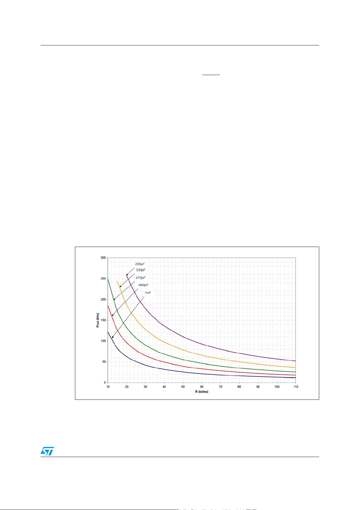
In order to fix the run frequency and the preheating frequency, the following curves can be
used. Each curve is related with a particular capacitor value, therefore a capacitor value
must be firstly chosen. The resistances corresponding Frun and Fpre can be graphically
found and are respectively Rrun and the parallel between Rrun and Rpre.
Figure 16. Oscillator characteristic curves
31/41
Page 32

Designing with L6585DE AN2870
A more accurate procedure can be followed considering that the reported curves can be
represented by the following equation (f in kHz and R in k
Ω):
Equation 40
k
f =
e
()
R
In particular the constant, k, and the exponent, e, can be calculated for a given Cosc
(expressed in pF) as follows:
Equation 41
3
C
OSC
106.499k⋅
872.0
=
()
Equation 42
1e −=
Figure 17. (A) k parameter versus Cosc (pF) Figure 17. (B) e parameter versus Cosc (pF)
33.1
OSC
581.0
()
C
Firstly k and e should be found and then R can be calculated as follows:
Equation 43
1
e
⎞
⎛
k
⎟
run
⎜
=
⎟
⎜
f
run
⎠
⎝
1
e
⎛
⎞
k
⎜
R//R
=
runpre
⎟
⎜
⎟
f
pre
⎝
⎠
R
32/41
Page 33

AN2870 Designing with L6585DE
⋅
=
(
⋅
=
The ignition time is equal to the time the capacitor Cign is charged by the RF current and the
EOI leakage current. A precise calculation of this parameter is not needed. It’s
approximately equal to:
Equation 44
CR3T =
ignpreign
Preheating time and protection time are related to Tch cycle:
Equation 45
pre
C
D
I
TCH
+=
63.4T
63.4
⎞
⎛
lnCR
DD
⎟
⎜
5.1
⎠
⎝
Equation 46
C269740T
Dprot
Half bridge design
When resonant network works in inductive region, half bridge MOSFETs switch at zero
voltage switching condition.
This implies that high side and low side MOSFETs experience mainly conduction losses
because of their on state resistance.
Equation 47
2
)
IRP ⋅=
rmson,dscond
I
can be considered as per Eq 38 or can be calculated considering that the waveform
rms
seen during an on time is a sinusoid having a frequency equal to resonance frequency.
From thermal consideration the maximum R
In order to drive correctly the high side MOSFET, a suitable boostrap capacitor is needed.
can be calculated.
ds,on
The size of the boostrap capacitor can be calculated considering the allowed V
total gate capacitance of the High side MOSFET and the R
of the integrated boostrap
on
drop, the
gs
diode.
In steady state, during the ON time of the low side transistor the bootstrap capacitor stores
charges:
Equation 48
VCQ
ccbootboot
During the ON time of the high side transistor, the charges stored in bootstrap capacitor are
shared with total gate capacitance, causing a voltage drop:
33/41
Page 34

Designing with L6585DE AN2870
Equation 49
Q
CC
bootgate
boot
=+
VV
Δ−
cc
These charges must be replaced during the subsequent ON time of the low side transistor:
Equation 50
⎛
⎡
−⋅−=
ln1CRT =
⎢
bootonboot
⎢
⎣
⎤
⎞
⎛
Δ
V
⎟
⎜
⎥
⎟
⎜
V
⎥
⎠
⎝
⎦
1
⎜
<
⎜
⎝
−
⋅
f2
precc
⎞
⎟
TT
⎟
⎠
min,onDeadTime
End of life detection
Blocking capacitor to GND configuration:
In case of blocking capacitor to ground configuration the tracking mode is suggested. In
order to set this mode a resistor placed between EOLP and GND is needed: its value has to
be chosen as follows:
● 220 kΩ < R
● 22 kΩ < R
EOL pin biasing proceeds as follows:
The blocking capacitor mean voltage is half of the PFC output voltage and the CTR pin
voltage is equal to:
Equation 51
Therefore the voltage divider connected between C
factor equal to:
< 270 kΩ → VW = 240 mV
eolp
< 27 kΩ → VW = 150 mV
eolp
CTR
V
out
4.3V ⋅=
V
OVP
and EOL pin should have a divider
block
Equation 52
k =
eol
A capacitor placed in parallel with the lower resistor and placed near the IC helps to keep
low the high frequency residual noise.
34/41
V2
⋅
CTR
=
V
8.6
V
OVPout
Page 35

AN2870 Designing with L6585DE
Figure 18. EOL - C
block
to ground
Lamp to GND configuration:
In case of lamp to ground configuration the fix reference mode is suggested.
In order to set this mode a resistor placed between EOLP and GND is needed: its value has
to be chosen as follows:
● 75 kΩ < R
● 620 kΩ < R
The EOL pin biasing proceeds as follows:
< 91kΩ → window amplitude = 240 mV
eolp
→ window amplitude = 720 mV
eolp
A voltage shift is needed in order to detect a null value with a positive referenced
comparator: two Zener diodes are requested.
The current capability of EOL pin is equal to 5.5 µA, therefore the minimum Zener voltage
that guarantees accuracy of the measurement is 8 V.
35/41
Page 36

Designing with L6585DE AN2870
Figure 19. EOL - lamp to ground
Consider the case of positive going lamp voltage mean value (VK): the maximum VK allowed
value is equal to:
Equation 53
VVV5.2V +++=
K
max
2F1zW
In the opposite case it will be:
Equation 54
VVV5.2V −−−=
K
min
1F2zW
In order to have a symmetrical behavior, the absolute values of the two voltages have to be
equal.
This brings to the following relation:
Equation 55
⎛
−=
V
K
max
V
⎜
⎝
V5.2
W
VV5.22
⎞
⎟
K
min
⎠
V
V
V
V
2z
2F
1z
V
−=⋅⇒
1z
V5.2
W
+++−=+++⇒
1F
2z
The difference of the Zener voltages has to be equal to 5V: twice the reference voltage.
36/41
Page 37

AN2870 Designing with L6585DE
(
⋅⋅=
The maximum deviation of the mean voltage of the lamp, V
lamp,EOL
, depends on the lamp
type (e.g. is 15 V for T5-54W lamp).
The following relation can be used to calculate the correct value of the divider's resistors
(R
Ehi
and R
Elo
)
Equation 56
)
IIRVV
+⋅−=
K
max
max
VV
K
−=
EOL,lamp
EOLREloEhiEOL,lamp
RV
⋅
EhiEOL,lamp
RR
+
EloEhi
Ehi
A5.5R
μ⋅−
The value of filtering capacitor should be calculated in order to have a cutoff frequency
equal to at least one hundreds of run frequency.
IC power supply design
L6585DE can be supplied by means of either external source, auxiliary winding on PFC
choke or charge pump connected to the middle point of half bridge. The most used method
is the charge pump connected to the middle point of the half bridge.
The charge pump must be able to deliver the correct current to the IC. I
half bridge and PFC driver switching activities. Typical values of I
CC
Figure 20.
The current is delivered by the capacitor during the edges of the middle point of the half
bridge. The slope of these edges is also related to the recovery time of the body diode of the
MOSFETs and to the capacitor itself. Assuming a linear slope the instantaneous current
delivered by the capacitor will be:
depends on both
CC
are reported on
Equation 57
V
OUT
CI =
cppk,cp
T
rise
Equation 58
IfTII ≥
ccrunrisepk,cpcp
The diode connected to ground is a Zener diode (15 V is the suggested value): it limits the
voltage across the Vcc pin avoiding an extra stress of the internal active clamp. In order to
limit the current flowing into this diode, when it is directly biased, a low value resistor is
placed in series with the capacitor.
A bigger capacitor (>1 µF) and a 100 nF ceramic capacitor placed near the IC are needed to
filter the Vcc voltage.
At start up the current is sunk from rectified mains and delivered to the IC through a resistor
path. This resistor is chosen in order to guarantee the minimum quiescent current required
by L6585DE (370 µA). Its value influences also the start-up time because it had to charge
the electrolytic capacitor connected to Vcc.
37/41
Page 38

Designing with L6585DE AN2870
Figure 20. Current consumption vs PFC frequency
38/41
Page 39

AN2870 Designing with L6585DE
4.3 PCB hints
The following rules, considered during the PCB design, help to optimize the performance of
the L6585DE.
1. In a board containing both PFC and Ballast section four different ground potentials are
present:
a) PFC signal ground,
b) PFC power ground
c) Ballast signal ground and
d) Ballast power ground.
These traces are usually kept separate and connected together in correspondence of a low
impedance node (the negative terminal of bulk capacitor). A similar rule has to be followed
in the L6585DE: power grounds are to be kept separate and connected to the negative
terminal of the bulk capacitor, signal grounds should be firstly routed to the pin GND (15)
and then the pin 15 is connected to the negative terminal of bulk capacitor. It is very
important that the ground trace relevant to C
GND pin as shortly as possible.
2. Ballast PCBs are usually long and narrow, therefore current loops are to be minimized
in order to reduce the electromagnetically induced interference between PFC stage
and Ballast Stage. This is very important when wide range application has to be
implemented.
3. Regions surrounding the gap of the chokes are usually very noisy therefore signal and
ground traces shouldn’t pass underneath these regions.
4. Traces that connect the gates of the MOSFETs, the OUT pin and the charge pump
components are affected by voltages that vary with very fast edges. They can
capacitively induce noise to closest traces. Therefore if a signal has to pass near these
nodes an increased distance between traces or, eventually, a ground shield has to be
considered.
5. Ground pin of shunt components should be placed as close as possible to star
connection point or, at least, close together, this avoids errors reading the voltage
across them and current sense traces has to be kept as short as possible in order to
avoid HF noise induction. In the second case is preferable to connect signal GND to the
ground of the shunts instead of the star point.
6. Bootstrap capacitor and Vcc ceramic capacitor have to be placed as close as possible
to relevant pins.
7. Error amplifier feedback network must be small and placed near the IC in order to
reduce any loop that can couple radio interference.
8. The drain of the PFC MOSFET, the anode of Boost Diode and the PFC choke are
connected together as close as possible. In fact this node experienced very fast edges
and also very high currents.
, RRF and C
OSC
is connected directly to the
PRE
39/41
Page 40

Revision history AN2870
5 Revision history
Table 2. Document revision history
Date Revision Changes
26-Mar-2009 1 Initial release
40/41
Page 41

AN2870
Please Read Carefully:
Information in this document is provided solely in connection with ST products. STMicroelectronics NV and its subsidiaries (“ST”) reserve the
right to make changes, corrections, modifications or improvements, to this document, and the products and services described herein at any
time, without notice.
All ST products are sold pursuant to ST’s terms and conditions of sale.
Purchasers are solely responsible for the choice, selection and use of the ST products and services described herein, and ST assumes no
liability whatsoever relating to the choice, selection or use of the ST products and services described herein.
No license, express or implied, by estoppel or otherwise, to any intellectual property rights is granted under this document. If any part of this
document refers to any third party products or services it shall not be deemed a license grant by ST for the use of such third party products
or services, or any intellectual property contained therein or considered as a warranty covering the use in any manner whatsoever of such
third party products or services or any intellectual property contained therein.
UNLESS OTHERWISE SET FORTH IN ST’S TERMS AND CONDITIONS OF SALE ST DISCLAIMS ANY EXPRESS OR IMPLIED
WARRANTY WITH RESPECT TO THE USE AND/OR SALE OF ST PRODUCTS INCLUDING WITHOUT LIMITATION IMPLIED
WARRANTIES OF MERCHANTABILITY, FITNESS FOR A PARTICULAR PURPOSE (AND THEIR EQUIVALENTS UNDER THE LAWS
OF ANY JURISDICTION), OR INFRINGEMENT OF ANY PATENT, COPYRIGHT OR OTHER INTELLECTUAL PROPERTY RIGHT.
UNLESS EXPRESSLY APPROVED IN WRITING BY AN AUTHORIZED ST REPRESENTATIVE, ST PRODUCTS ARE NOT
RECOMMENDED, AUTHORIZED OR WARRANTED FOR USE IN MILITARY, AIR CRAFT, SPACE, LIFE SAVING, OR LIFE SUSTAINING
APPLICATIONS, NOR IN PRODUCTS OR SYSTEMS WHERE FAILURE OR MALFUNCTION MAY RESULT IN PERSONAL INJURY,
DEATH, OR SEVERE PROPERTY OR ENVIRONMENTAL DAMAGE. ST PRODUCTS WHICH ARE NOT SPECIFIED AS "AUTOMOTIVE
GRADE" MAY ONLY BE USED IN AUTOMOTIVE APPLICATIONS AT USER’S OWN RISK.
Resale of ST products with provisions different from the statements and/or technical features set forth in this document shall immediately void
any warranty granted by ST for the ST product or service described herein and shall not create or extend in any manner whatsoever, any
liability of ST.
ST and the ST logo are trademarks or registered trademarks of ST in various countries.
Information in this document supersedes and replaces all information previously supplied.
The ST logo is a registered trademark of STMicroelectronics. All other names are the property of their respective owners.
© 2009 STMicroelectronics - All rights reserved
STMicroelectronics group of companies
Australia - Belgium - Brazil - Canada - China - Czech Republic - Finland - France - Germany - Hong Kong - India - Israel - Italy - Japan -
Malaysia - Malta - Morocco - Singapore - Spain - Sweden - Switzerland - United Kingdom - United States of America
www.st.com
41/41
 Loading...