

Page 1
AN2866
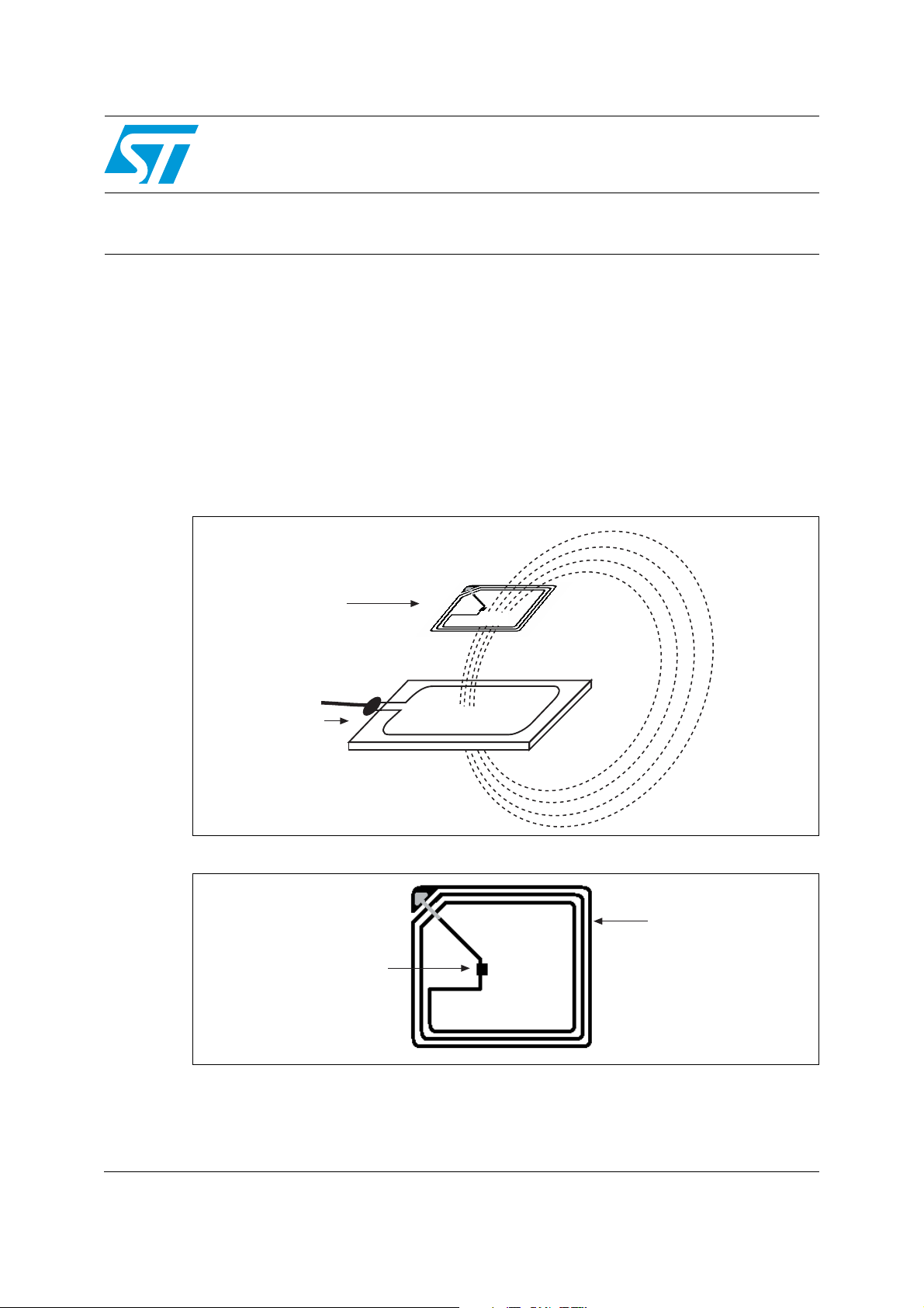
ai15802
Antenna
Chip
Application note
How to design a 13.56 MHz
customized tag antenna
Introduction
RFID (radio-frequency identification) tags extract all of their power from the reader’s field.
The tags’ and reader’s antennas form a system of coupled inductances as shown in
Figure 1. The loop antenna of the tag acts as a transformer’s secondary.
The efficient transfer of energy from the reader to the tag depends on the precision of the
parallel resonant RLC loop antennas tuned to the carrier frequency (usually 13.56 MHz).
The purpose of this application note is to give a step-by-step procedure to easily design a
customized tag antenna.
Figure 1. RFID tag coupled to a reader’s magnetic field
Tag
Reader
Figure 2. An antenna designed for a specific chip and frequency
ai15802
January 2009 Rev 1 1/24
www.st.com
Page 2

Contents AN2866
Contents
1 Simplified equivalent inlay circuit. . . . . . . . . . . . . . . . . . . . . . . . . . . . . . . 5
2 Equivalent inlay circuit . . . . . . . . . . . . . . . . . . . . . . . . . . . . . . . . . . . . . . . 6
3 Calculating the antenna coil inductance . . . . . . . . . . . . . . . . . . . . . . . . . 8
4 Designing the antenna coil . . . . . . . . . . . . . . . . . . . . . . . . . . . . . . . . . . . 10
4.1 Inductance of a circular loop . . . . . . . . . . . . . . . . . . . . . . . . . . . . . . . . . . 10
4.2 Inductance of a spiral coil . . . . . . . . . . . . . . . . . . . . . . . . . . . . . . . . . . . . . 10
4.3 Inductance of an antenna with square coils . . . . . . . . . . . . . . . . . . . . . . . 10
5 Contactless measurement method . . . . . . . . . . . . . . . . . . . . . . . . . . . . 14
5.1 Antenna coil prototype verification with an analyzer . . . . . . . . . . . . . . . . 14
5.1.1 Preparing the equipment and connections . . . . . . . . . . . . . . . . . . . . . . 14
5.1.2 Instructions . . . . . . . . . . . . . . . . . . . . . . . . . . . . . . . . . . . . . . . . . . . . . . 14
5.2 Antenna coil prototype verification without an analyzer (first
method) . . . . . . . . . . . . . . . . . . . . . . . . . . . . . . . . . . . . . . . . . . . . . . . . . . 15
5.2.1 Preparing the equipment and connections . . . . . . . . . . . . . . . . . . . . . . 15
5.2.2 Instructions . . . . . . . . . . . . . . . . . . . . . . . . . . . . . . . . . . . . . . . . . . . . . . 16
6 Non-contactless (contact) measurement method . . . . . . . . . . . . . . . . 18
6.1 Without an analyzer (second method) . . . . . . . . . . . . . . . . . . . . . . . . . . . 18
6.1.1 Preparing the equipment and connections . . . . . . . . . . . . . . . . . . . . . . 18
6.1.2 Instructions . . . . . . . . . . . . . . . . . . . . . . . . . . . . . . . . . . . . . . . . . . . . . . 19
6.1.3 Example using an LRI2K device . . . . . . . . . . . . . . . . . . . . . . . . . . . . . . 19
7 Frequency versus application: recommendations . . . . . . . . . . . . . . . 22
8 Revision history . . . . . . . . . . . . . . . . . . . . . . . . . . . . . . . . . . . . . . . . . . . 23
2/24
Page 3

AN2866 List of tables
List of tables
Table 1. Antenna coil inductances for different C
Table 2. K1 & K2 values according to layout . . . . . . . . . . . . . . . . . . . . . . . . . . . . . . . . . . . . . . . . . . 11
Table 3. Document revision history . . . . . . . . . . . . . . . . . . . . . . . . . . . . . . . . . . . . . . . . . . . . . . . . . 23
values at a given tuning frequency . . . . . . . . . . 8
tun
3/24
Page 4

List of figures AN2866
List of figures
Figure 1. RFID tag coupled to a reader’s magnetic field . . . . . . . . . . . . . . . . . . . . . . . . . . . . . . . . . . . 1
Figure 2. An antenna designed for a specific chip and frequency . . . . . . . . . . . . . . . . . . . . . . . . . . . . 1
Figure 3. Equivalent circuit of a chip and its antenna . . . . . . . . . . . . . . . . . . . . . . . . . . . . . . . . . . . . . 5
Figure 4. Equivalent circuit of a chip, its antenna (modeled with a series
resistance) and connections . . . . . . . . . . . . . . . . . . . . . . . . . . . . . . . . . . . . . . . . . . . . . . . . 6
Figure 5. Equivalent circuit of a chip, its antenna (modeled with a parallel
resistance) and connections . . . . . . . . . . . . . . . . . . . . . . . . . . . . . . . . . . . . . . . . . . . . . . . . . 6
Figure 6. Simplified equivalent circuit of a chip, its antenna and connections . . . . . . . . . . . . . . . . . . . 7
Figure 7. Antenna design procedure . . . . . . . . . . . . . . . . . . . . . . . . . . . . . . . . . . . . . . . . . . . . . . . . . . 9
Figure 8. Spiral coil . . . . . . . . . . . . . . . . . . . . . . . . . . . . . . . . . . . . . . . . . . . . . . . . . . . . . . . . . . . . . . 10
Figure 9. Square coils . . . . . . . . . . . . . . . . . . . . . . . . . . . . . . . . . . . . . . . . . . . . . . . . . . . . . . . . . . . . 11
Figure 10. User interface screen of the planar rectangular coil inductance calculator. . . . . . . . . . . . . 12
Figure 11. Rectangular planar antennas . . . . . . . . . . . . . . . . . . . . . . . . . . . . . . . . . . . . . . . . . . . . . . . 13
Figure 12. Measurement equipment . . . . . . . . . . . . . . . . . . . . . . . . . . . . . . . . . . . . . . . . . . . . . . . . . . 14
Figure 13. Resonance traces of the prototype at different powers . . . . . . . . . . . . . . . . . . . . . . . . . . . 15
Figure 14. ISO standard loop antenna. . . . . . . . . . . . . . . . . . . . . . . . . . . . . . . . . . . . . . . . . . . . . . . . . 16
Figure 15. Without an analyzer: first measurement method . . . . . . . . . . . . . . . . . . . . . . . . . . . . . . . . 16
Figure 16. Oscilloscope views . . . . . . . . . . . . . . . . . . . . . . . . . . . . . . . . . . . . . . . . . . . . . . . . . . . . . . . 17
Figure 17. Synthesis of resonance traces for different voltages . . . . . . . . . . . . . . . . . . . . . . . . . . . . . 17
Figure 18. Measurement circuit . . . . . . . . . . . . . . . . . . . . . . . . . . . . . . . . . . . . . . . . . . . . . . . . . . . . . . 18
Figure 19. Determining the resonance frequency . . . . . . . . . . . . . . . . . . . . . . . . . . . . . . . . . . . . . . . . 19
Figure 20. Coil samples . . . . . . . . . . . . . . . . . . . . . . . . . . . . . . . . . . . . . . . . . . . . . . . . . . . . . . . . . . . . 20
Figure 21. Coil characterization . . . . . . . . . . . . . . . . . . . . . . . . . . . . . . . . . . . . . . . . . . . . . . . . . . . . . . 20
Figure 22. New coil samples . . . . . . . . . . . . . . . . . . . . . . . . . . . . . . . . . . . . . . . . . . . . . . . . . . . . . . . . 21
Figure 23. Second coil characterization. . . . . . . . . . . . . . . . . . . . . . . . . . . . . . . . . . . . . . . . . . . . . . . . 21
Figure 24. Best antenna coil prototype . . . . . . . . . . . . . . . . . . . . . . . . . . . . . . . . . . . . . . . . . . . . . . . . 21
4/24
Page 5
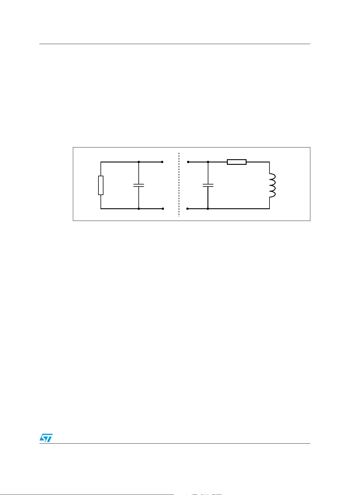
AN2866 Simplified equivalent inlay circuit
ai15804
R
chip
C
tun
A
B
R
ant
C
ant
L
ant
Chip Antenna
1 Simplified equivalent inlay circuit
The chip and its antenna can be symbolized using their equivalent electrical circuit.
Figure 3 shows the equivalent electrical circuit of the chip (parallel association of a
resistance which emulates the current consumption of the chip and a capacitance added to
the chip to ease tuning).
The antenna is a wire, so its equivalent electrical circuit is a wire with a resistance
symbolized by R
C
is the representation of parasitic elements (produced by the bridge).
ant
Figure 3. Equivalent circuit of a chip and its antenna
. The antenna also has an inductance denoted by L
ant
. The capacitance
ant
5/24
Page 6
Equivalent inlay circuit AN2866
ai15805
R
chip
C
tun
A
B
R
s_ant
C
ant
L
ant
Chip Antenna
R
1con
C
con
R
2con
Connection
ai15841
R
chip
C
tun
A
B
R
p_ant
C
ant
L
ant
Chip Antenna
R
1con
C
con
R
2con
Connection
2 Equivalent inlay circuit
The schematic shown in Figure 3 is but a first approach to the problem because it does not
take into account the connection between the chip and the antenna. The assembly phase of
the chip onto the antenna may lead to the introduction of parasitic elements. These parasitic
elements are symbolized by two resistances and a capacitance as shown in Figure 4 and
Figure 5.
The equivalent circuit of the antenna may include either a series (see Figure 4) or a parallel
(see Figure 5) resistance.
Figure 4. Equivalent circuit of a chip, its antenna (modeled with a series
resistance) and connections
Figure 5. Equivalent circuit of a chip, its antenna (modeled with a parallel
resistance) and connections
The symbols in Figure 4 and Figure 5 correspond to:
R
: current consumption of the chip for a given power value
chip
C
: tuning capacitance of the chip
tun
R
: equivalent parasitic resistance generated by the connection between the chip and
con
the antenna
C
: equivalent parasitic capacitance generated by the connection between the chip and
con
the antenna
C
: equivalent parasitic capacitance of the antenna coil
ant
: Antenna coil series resistance
R
s_ant
R
: Antenna coil parallel resistance
p_ant
L
: Antenna coil inductance
ant
6/24
Page 7
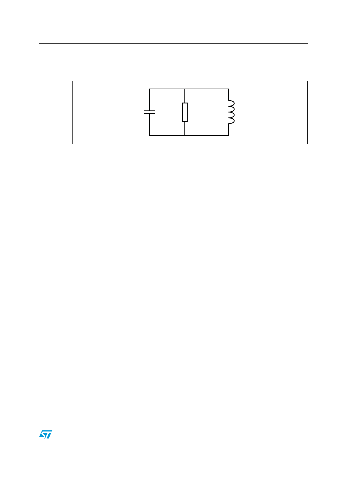
AN2866 Equivalent inlay circuit
ai15806
C
tun
L
ant
R
eq
R
eq
R
chipRp_ant
×
R
chipRp_ant
+
------------------------------------- -=
R
p_ant
R
s_ant
1
L
ant
ω×
R
s_ant
-------------------- -
⎝⎠
⎛⎞
2
+
⎝⎠
⎛⎞
×=
This equivalent circuit (Figure 4) can also be simplified as illustrated in Figure 6 (use the
simplified circuit for calculations).
Figure 6. Simplified equivalent circuit of a chip, its antenna and connections
R
is calculated as follows:
eq
with where ω is the angular frequency.
7/24
Page 8
Calculating the antenna coil inductance AN2866
f
0
1
2π L
antCtun
⋅
---------------------------------------- -=
L
ant
1
2πf
0
()2C
tun
⋅
------------------------------------- -=
Q
R
eq
2π f0L
ant
⋅⋅
------------------------------------=
L
ant
1
2π 13.56 MHz×()
2
21 pF⋅
------------------------------------------------------------------------ - 6.56 µH==
3 Calculating the antenna coil inductance
The resonant frequency f0 of a parallel resonant LC circuit can be calculated by:
The coil inductance at the carrier frequency resonance is: .
The quality factor Q of the simplified circuit is calculated as follows: .
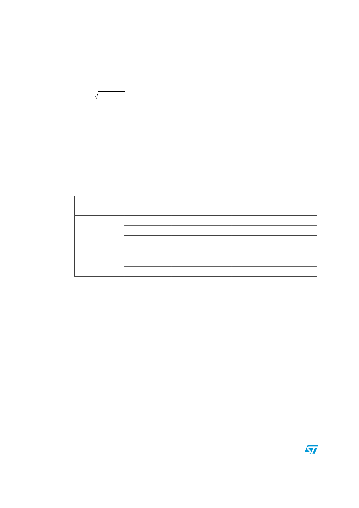
Example of the calculation of an antenna coil inductance:
Table 1. Antenna coil inductances for different C
frequency
values at a given tuning
tun
Product C
tun
(pF)
Tuning frequency
(MHz)
Antenna coil inductance (µH)
21 13.56 6.56
28.5 13.56 4.83
LR (long-range)
23.5 13.56 5.86
97 13.56 1.42
64 13.56 2.15
SR (short range)
64 14.40 1.90
Figure 7 describes the steps of the antenna design procedure that gives an easy and
reliable method of designing an antenna coil prototype.
This procedure uses the C
capacitance of the chip, a software tool called antenne.exe,
tun
and tools to produce antenna coil prototypes.
By determining dimensions and values, the execution of the first run gives the best out of
three coils meeting the requirements. Usually, the best results appear after the second run.
8/24
Page 9

AN2866 Calculating the antenna coil inductance
Compute L
ant
based on
C
tun
and f
0
Determining the parameters
for 2nd run
Run 2
Run 1
ai15807
Define the antenna's
mechanical dimensions
Definition of the antenna matrix
Design matrix (L
ant
; L
ant
+5%; L
ant
–5%)
Production of coil prototypes
Characterization of coil
prototypes
Determining the best coil
parameters
Definition of the antenna matrix
Design matrix (L
ant
; L
ant
+2%; L
ant
–2%)
Production of coil prototypes
Characterization of coil
prototypes
Determining the best coil
parameters
Select an RFID product
(SR or LR)
Select a C
tun
value
(see available values in product datasheet)
Fix the f0 target
Figure 7. Antenna design procedure
9/24
Page 10

Designing the antenna coil AN2866
L
antμ0
N
1.9
r×
r
r
0
----
⎝⎠
⎛⎞
ln××=
L
ant
31.33 μ0× N2×
d
8d 11c+
---------------------- -
×=
L
ant
K1 μ0× N2×
d
1K2 p⋅+
--------------------------- -
×=
4 Designing the antenna coil
In the paragraphs below, the antenna inductance is calculated for different types of antenna
coils.
4.1 Inductance of a circular loop
, where:
● r is the mean coil radius in millimeters
● r
is the wire diameter in millimeters
0
● N is the number of turns
● µ
● L is measured in Henry
4.2 Inductance of a spiral coil
= 4π · 10–7 H/m
0
, where:
● d is the mean coil diameter in millimeters
● c is the thickness of the winding in microns
● N is the number of turns
● µ
● L is measured in Henry
= 4π · 10–7 H/m
0
Figure 8. Spiral coil
4.3 Inductance of an antenna with square coils
, where:
● d is the mean coil diameter
d = (d
● p = (d
● K1 and K2 depend on the layout (refer to Tab l e 2 for values)
+ din)/2 in millimeters, where: d
out
– din)/(d
out
+ din) in millimeters
out
= outer diameter
out
d
= inner diameter
in
ai15812
10/24
Page 11

AN2866 Designing the antenna coil
L
antL0
M
∑
+=
L
0
L
j
j1=
s
∑
=
Figure 9. Square coils
Table 2. K1 & K2 values according to layout
Layout K1 K2
Square 2.34 2.75
Hexagonal 2.33 3.82
Octagonal 2.25 3.55
The software tool (antenne.exe) uses the Grover method (see Equation 1: : Grover method)
to calculate the inductance of rectangular planar antennas. Figure 10 shows the software
user interface.
The software gives a good approximation of the antenna inductance L
. This can be
ant
checked by comparing the software results to measurements of the inductance of a real
antenna on an impedance meter.
Equation 1: Grover method
, where:
● M is the mutual inductance between each of the antenna segments
● L
is as defined in Equation 2
0
Equation 2: , where:
● s is the number of segments
● L
is the self inductance of each segment
j
11/24
Page 12

Designing the antenna coil AN2866
Figure 10. User interface screen of the planar rectangular coil inductance calculator
Examples:
The following antenna parameters have to be fed to the software to compute the antenna
coil inductance:
● the number of turns
● the number of segments
● w: the conductor width in millimeters
● s: the conductor spacing in millimeters
● the conductor thickness in micrometers)
● Length in millimeters
● Width in millimeters
The number of turns is incremented each time a segment is added to a complete turn.
12/24
Page 13

AN2866 Designing the antenna coil
Width
Length
s
w
1
1
810
3 turns, 10 segments 2 turns, 8 segments
ai15815
thickness
(cross-section)
Figure 11. Rectangular planar antennas
Once the antenna coil inductance has been calculated, a prototype coil is realized. The
value of the so-obtained prototype must then be validated by measurement. This can be
done using either a contactless or a non-contactless method. Section 5 and Section 6
describe these methods.
13/24
Page 14

Contactless measurement method AN2866
5 Contactless measurement method
This section describes a contactless verification method of antenna coil prototypes. The
results presented here are based on a short-range (SR) tag antenna initially designed to
have the following characteristics:
● Antenna dimensions: 38 mm × 38 mm (A3)
● Tuning frequency: 14.4 MHz
5.1 Antenna coil prototype verification with an analyzer
Equipment needed:
● Impedance analyzer
● Prototype antenna coil
● Reference capacitor
The equivalent circuit of the antenna coil can be determined using the appropriate
measuring instruments (see Figure 12) and following the instructions described in
Section 5.1.2.
5.1.1 Preparing the equipment and connections
The reference capacitor is used to simulate the presence of the chip on the prototype coil.
Connect it to the coil using an appropriate test fixture (to have as little interference as
possible). The coil is now ready for measurements.
This example measurement uses the 7405-901 Eaton/Alitech (singer) 6 cm loop probe
connected to the reflection interface of the Hp 8712ET network analyzer.
Figure 12. Measurement equipment
Network analyser Loop probe Antenna coil prototype
5.1.2 Instructions
The network analyzer must be in reflection mode.
Measurement conditions (case of a short-range RFID tag):
● Start frequency: 10 MHz
End frequency: 15 MHz
● Power: –10 dB (which is the minimum detection level, the lowest field required to power
the chip)
+ reference capacitor
ai15816
The coil must be in the field generated by the network analyzer via the loop probe
(measurements made at about 0.5 cm from the probe).
14/24
Page 15

AN2866 Contactless measurement method
power at 10 dB
power at 0 dB
power at –10 dB
power at –20 dB
power at –30 dB
Figure 13. Resonance traces of the prototype at different powers
12.5 13 13.5 14 14. 5 15 15. 5
–1
–3
–5
–7
–9
–11
ai15829
5.2 Antenna coil prototype verification without an analyzer (first
method)
There is another method of measuring the antenna coil inductance, that does not require an
impedance analyzer.
Equipment needed:
● Signal generator
● Oscilloscope
● Reference capacitor
● Loop antenna
The equivalent circuit of the antenna coil can be determined using the appropriate
measuring instruments (see Figure 14) and following the instructions described in
Section 5.2.2.
5.2.1 Preparing the equipment and connections
The reference capacitor simulates the presence of the chip on the prototype coil. Connect it
to the coil using an appropriate test fixture (to have as little interference as possible). The
antenna coil is now ready for measurements.
Connect an ISO 10373-7 standard loop antenna (see Figure 13) to the signal generator,
(you may need an additional series resistor depending on the power you want to generate).
The loop antenna can now generate a field.
15/24
Page 16

Contactless measurement method AN2866
Synchronization frequency
Tag to be measured
1 loop antenna.
Must be tuned between
50 and 60 MHz
Q factor measurement scheme
ai15819
Signal generator
Oscilloscope
Figure 14. ISO standard loop antenna
ISO/IEC 7810 ID-1 outline
72 mm × 42 mm coil
1 turn
To make the analysis, connect a second ISO standard loop antenna (see Figure 14) (with a
50 Ω input resistance) to the oscilloscope, and place it in the field generated by the first loop
antenna as shown in Figure 15. The coil prototype is coupled to the signal generator (no
contact).
Figure 15. Without an analyzer: first measurement method
connections
i15819
The measurement method is now operational.
5.2.2 Instructions
To make the measurements place the prototype coil right in the transmission loop probe
(with the reception loop probe at about 0.5 cm from the prototype coil).
Generate a signal (sine 13.56 MHz) at a voltage of 0.25 V (corresponds approximately to a
power of –10 dB). Then vary the transmission frequency in order to obtain as high a signal
level as possible on the reception side. Use the oscilloscope to determine the signal level
and thus determine the resonant frequency).
Figure 16 shows two signal waveforms (the standard loop antenna transmission in green
and the standard loop antenna reception in red) at different transmission frequencies.
16/24
Page 17

AN2866 Contactless measurement method
0
0.5
1
1.5
2
2.5
3
3.5
12.5 13 13.5 14 14.5
100 mV
200 mV
300 mV
400 mV
Figure 16. Oscilloscope views
Transmission: 0.2 V sine (13.56 MHz)
Reception: 0.1 V sine (13.56 MHz)
Transmission: 0.2 V sine (14.3 MHz)
Reception: 0.2 V sine (14.3 MHz)
ai15820
Figure 17 provides a synthesis of the measurements made. It is obtained by plotting
characteristic points for different frequencies at a given voltage. Each resonance trace
represents a synthesis for a definite voltage transmission.
Figure 17. Synthesis of resonance traces for different voltages
ai15821
Note: 1 Without a tag: the scope trace must be as flat as possible. It is the reason why the antenna
connected to the generator must not be tuned at 13.56 MHz.
2 With a tag on the antenna: the scope trace shows the resonance of the system without any
contact.
17/24
Page 18

Non-contactless (contact) measurement method AN2866
6 Non-contactless (contact) measurement method
This section describes a non-contactless verification method of antenna coil prototypes. The
results presented here are based on a short-range (SR) tag antenna initially designed to
have the following characteristics:
● Antenna dimensions: 38 mm × 38 mm (A3)
● Tuning frequency: 14.4 MHz
6.1 Without an analyzer (second method)
Equipment needed:
● Signal generator
● Oscilloscope
● Reference capacitor
● Loop antenna
The equivalent circuit of the antenna coil can be determined using the appropriate
measuring instruments (see Figure 18) and following the instructions described in
Section 6.1.2.
6.1.1 Preparing the equipment and connections
The reference capacitor simulates the presence of the chip. Connect it to the coil using an
appropriate test fixture (to generate as little interference as possible). The coil is now ready
for measurements.
To make the analysis, connect a second ISO standard loop antenna (see Figure 14) (with a
50 Ω input resistance) to the oscilloscope, and place it in the field generated by the first loop
antenna as shown in Figure 18.
Figure 18. Measurement circuit
47 kΩ
Signal generator
The measurement circuit is now operational.
C
tun
Oscilloscope
250 Msamples/s
ai15822
18/24
Page 19

AN2866 Non-contactless (contact) measurement method
50
150
250
350
450
550
12.5 13 13.5 14 14.5 15
MHz
mV
ai15824
L
ant
1
2π f
0
⋅()2C
tun
⋅
-------------------------------------------- - 6.56 µH==
6.1.2 Instructions
Measurements are made with the coil prototype physically connected to the signal
generator.
Generate a signal (sine 13.56 MHz) at a 10 V voltage. Then vary the transmission frequency
(from 12.5 MHz to 15 MHz), in order to obtain as high a signal level as possible on the
reception side. Use the oscilloscope to determine the signal level and thus determine the
resonant frequency (see Figure 19).
Figure 19. Determining the resonance frequency
6.1.3 Example using an LRI2K device
In this example, the selected device is a long-range RFID tag named LRI2K. The initial
design target for the inlay antenna is:
● Dimensions: the antenna must fit within an ISO ID1 format credit card
● Frequency tuning target: 13.6 MHz
Procedure
Follow the steps described below:
1. Choose the tuning capacitance of the product: 21 pF
2. Determine the objective Inductance:
3. Define the antenna’s mechanical dimensions: 45 × 75 (mm)
4. Definition of the test matrix: use the calculated L
close values depending on the precision required:
– 6.56 µH (L
– 6.88 µH (L
– 6.23 µH (L
5. Production of antenna coil samples:
ant
ant
ant
)
+5%)
–5%)
value, then, take two more or less
ant
19/24
Page 20

Non-contactless (contact) measurement method AN2866
L
ant
L
ant
()L
ant
5%+()+
2
---------------------------------------------------- - 6.72 µH==
Figure 20. Coil samples
6.56 µH (L
ant
)
6.88 µH (L
ant
+5%)
6.23 µH (L
ant
– 5%)
ai15824
6 . C h ara c t erizat i o n of a n t enna c o i l sam p l es
The coil samples are characterized using the Hp 8712ET analyzer in reflection mode
and the 7405-901 Eaton/Alitech (singer) 6 cm loop probe. The probe generates a field
and analyzes the response field.
Figure 21. Coil characterization
V
6.23 µH 6.56 µH 6.88 µH
F
13.56 MHz
ai15825
7. Determining the best coil parameter
Figure 21 shows that the ideal tuning is between L
ant
and L
ant
+5%.
The average of the two is given by:
8. Definition of the test matrix: use the new calculated L
value, then, take two more or
ant
less close values depending on the precision required:
– 6.72 µH (L
– 6.85 µH (L
– 6.58 µH (L
ant
ant
ant
)
+2%)
–2%)
9. Production of antenna coil samples:
20/24
Page 21

AN2866 Non-contactless (contact) measurement method
Figure 22. New coil samples
6.72 µH (L
ant
)
6.85 µH (L
ant
+2%)
6.58 µH (L
ant
–2%)
10. Characterization of the coil samples
As shown in Figure 23, the ideal tuning is close to L
ant
.
Figure 23. Second coil characterization
V
6.58 µH 6.72 µH 6.85 µH
F
13.56 MHz
ai15826
11. Conclusion: the best coil prototype is the one tuned at a little more than 6.72 µH
(illustrated in Figure 24).
Figure 24. Best antenna coil prototype
ai15827
ai15828
21/24
Page 22

Frequency versus application: recommendations AN2866
7 Frequency versus application: recommendations
Before designing the tag antenna it is important to know which frequency has to be used in
your application.
● Long-range (LR) products are usually tuned between 13.6 MHz and 13.7 MHz (for
distance optimization).
● Standard short-range SR products are usually tuned between 13.6 MHz and 13.9 MHz
(for distance optimization).
● Short-range products used as transport tickets are usually tuned between 14.5 MHz
and 15 MHz (for stack optimization).
These targeted frequencies should take into account the frequency shift due to the final
label material and environment. Let us take the example of a sticker tag with a paper label:
Paper and adhesive decrease the inlay antenna frequency by about 300 kHz. It is
therefore necessary to tune the initial inlay at about 13.9 MHz instead of the specified
13.6 MHz.
22/24
Page 23

AN2866 Revision history
8 Revision history
Table 3. Document revision history
Date Revision Changes
15-Jan-2008 1 Initial release.
23/24
Page 24

AN2866
Please Read Carefully:
Information in this document is provided solely in connection with ST products. STMicroelectronics NV and its subsidiaries (“ST”) reserve the
right to make changes, corrections, modifications or improvements, to this document, and the products and services described herein at any
time, without notice.
All ST products are sold pursuant to ST’s terms and conditions of sale.
Purchasers are solely responsible for the choice, selection and use of the ST products and services described herein, and ST assumes no
liability whatsoever relating to the choice, selection or use of the ST products and services described herein.
No license, express or implied, by estoppel or otherwise, to any intellectual property rights is granted under this document. If any part of this
document refers to any third party products or services it shall not be deemed a license grant by ST for the use of such third party products
or services, or any intellectual property contained therein or considered as a warranty covering the use in any manner whatsoever of such
third party products or services or any intellectual property contained therein.
UNLESS OTHERWISE SET FORTH IN ST’S TERMS AND CONDITIONS OF SALE ST DISCLAIMS ANY EXPRESS OR IMPLIED
WARRANTY WITH RESPECT TO THE USE AND/OR SALE OF ST PRODUCTS INCLUDING WITHOUT LIMITATION IMPLIED
WARRANTIES OF MERCHANTABILITY, FITNESS FOR A PARTICULAR PURPOSE (AND THEIR EQUIVALENTS UNDER THE LAWS
OF ANY JURISDICTION), OR INFRINGEMENT OF ANY PATENT, COPYRIGHT OR OTHER INTELLECTUAL PROPERTY RIGHT.
UNLESS EXPRESSLY APPROVED IN WRITING BY AN AUTHORIZED ST REPRESENTATIVE, ST PRODUCTS ARE NOT
RECOMMENDED, AUTHORIZED OR WARRANTED FOR USE IN MILITARY, AIR CRAFT, SPACE, LIFE SAVING, OR LIFE SUSTAINING
APPLICATIONS, NOR IN PRODUCTS OR SYSTEMS WHERE FAILURE OR MALFUNCTION MAY RESULT IN PERSONAL INJURY,
DEATH, OR SEVERE PROPERTY OR ENVIRONMENTAL DAMAGE. ST PRODUCTS WHICH ARE NOT SPECIFIED AS "AUTOMOTIVE
GRADE" MAY ONLY BE USED IN AUTOMOTIVE APPLICATIONS AT USER’S OWN RISK.
Resale of ST products with provisions different from the statements and/or technical features set forth in this document shall immediately void
any warranty granted by ST for the ST product or service described herein and shall not create or extend in any manner whatsoever, any
liability of ST.
ST and the ST logo are trademarks or registered trademarks of ST in various countries.
Information in this document supersedes and replaces all information previously supplied.
The ST logo is a registered trademark of STMicroelectronics. All other names are the property of their respective owners.
© 2009 STMicroelectronics - All rights reserved
STMicroelectronics group of companies
Australia - Belgium - Brazil - Canada - China - Czech Republic - Finland - France - Germany - Hong Kong - India - Israel - Italy - Japan -
Malaysia - Malta - Morocco - Singapore - Spain - Sweden - Switzerland - United Kingdom - United States of America
www.st.com
24/24
 Loading...