

Page 1

AN2865
Application note
STUSBCD01B configuration and operation
Introduction
With the ever-increasing number of mobile devices adopting the USB bus as the standard
communication port and source for recharging, a standardization of the characteristics of
the charging devices and methods to detect them is required to optimize the performance of
the charging process and reduce the risks of damaging standard USB ports.
The new USB battery charging specification provides rules and guidelines to follow when
designing new USB architectures capable of battery charging and when defining new
charging host ports. The specification also extends the range of current which can be drawn
from a USB port.
In order to be able to distinguish between this new class of USB ports, standard USB host
ports and dedicated chargers, the new specification also defines detection methods which
must be used to determine the right amount of current the portable device can draw from the
USB bus. This also guarantees backward compatibility with standard USB ports.
The STUSBCD01B is a USB charging detection IC developed on the base of the USB
battery charging specification which can be easily added in new platforms to provide them
with charging detection capability.
September 2009 Doc ID 15283 Rev 1 1/17
www.st.com
Page 2

Contents AN2865
Contents
1 STUSBCD01B description . . . . . . . . . . . . . . . . . . . . . . . . . . . . . . . . . . . . 3
2 Application circuit . . . . . . . . . . . . . . . . . . . . . . . . . . . . . . . . . . . . . . . . . . . 4
3 Interface and control pins . . . . . . . . . . . . . . . . . . . . . . . . . . . . . . . . . . . . 6
3.1 Status/method pin . . . . . . . . . . . . . . . . . . . . . . . . . . . . . . . . . . . . . . . . . . . 6
3.2 Detect pin . . . . . . . . . . . . . . . . . . . . . . . . . . . . . . . . . . . . . . . . . . . . . . . . . . 6
3.3 Default method pin . . . . . . . . . . . . . . . . . . . . . . . . . . . . . . . . . . . . . . . . . . . 7
4 Current sink detection method . . . . . . . . . . . . . . . . . . . . . . . . . . . . . . . . 8
5 Dedicated charger detection method . . . . . . . . . . . . . . . . . . . . . . . . . . 11
6 Software detection and hardware detection . . . . . . . . . . . . . . . . . . . . . 14
7 References . . . . . . . . . . . . . . . . . . . . . . . . . . . . . . . . . . . . . . . . . . . . . . . . 15
8 Revision history . . . . . . . . . . . . . . . . . . . . . . . . . . . . . . . . . . . . . . . . . . . 16
2/17 Doc ID 15283 Rev 1
Page 3

AN2865 STUSBCD01B description
1 STUSBCD01B description
The STUSBCD01B is the ideal solution for all mobile products using the USB bus for battery
charging. It can be used in all USB architectures (low-, full- or high-speed) where the
transceiver or the battery charger does not have smart charger detection. The
STUSBCD01B implements two different detection methods to distinguish between
dedicated chargers, charging host ports and standard host ports.
The device can be fully controlled through digital inputs (software detection mode) and is
also able to perform the charger detection automatically when the battery voltage is too low
to allow the application controller to be operative (hardware detection mode). A V
referred open-drain output (detect) is available for direct control over the USB charging
controller.
The STUSBCD01B also provides a clamping circuit which can be used to protect each USB
IC connected to the USB V
components and its power consumption is extremely low.
against overvoltage. The device requires few external
BUS
BAT
-
Doc ID 15283 Rev 1 3/17
Page 4
Application circuit AN2865
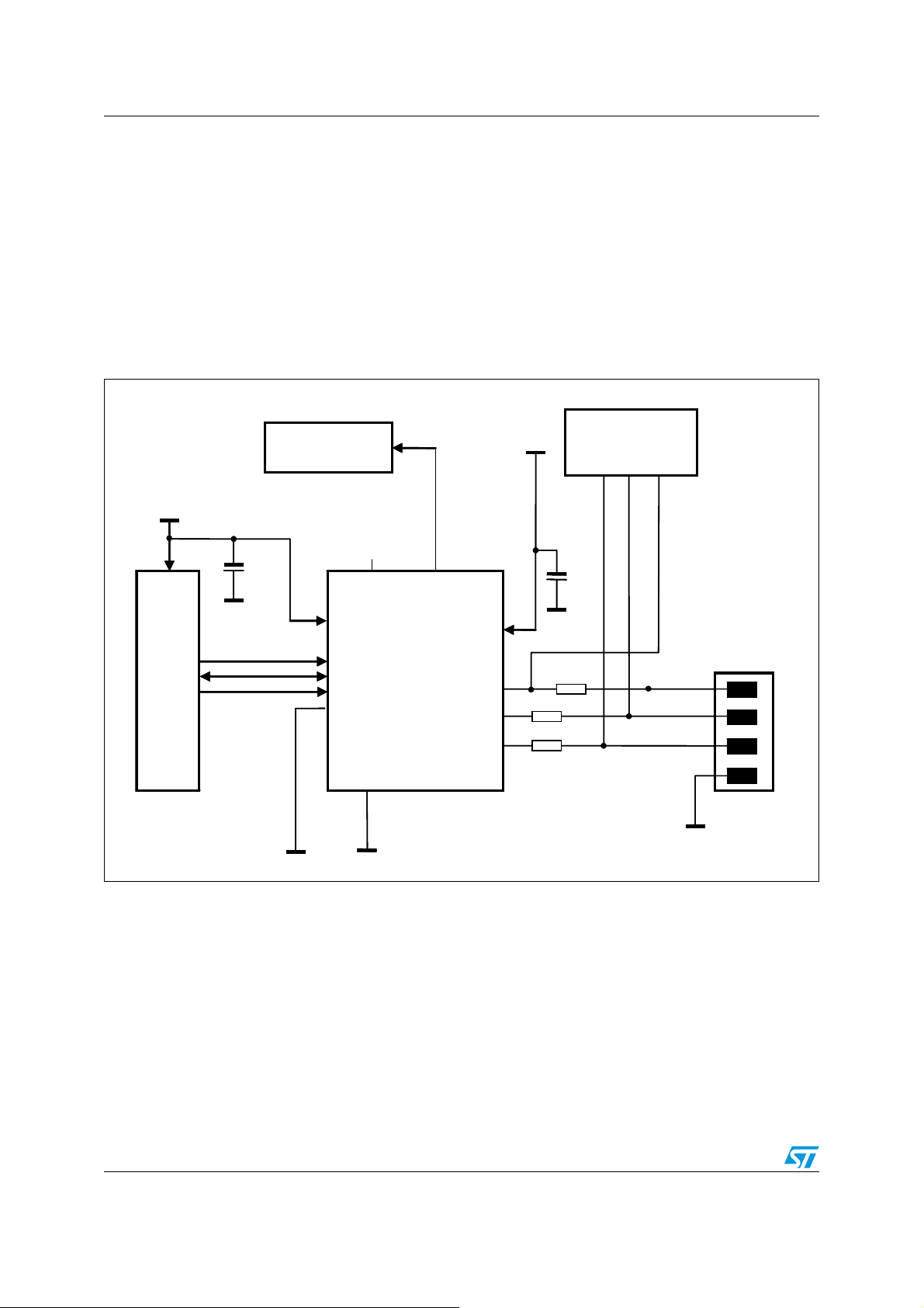
2 Application circuit
The STUSBCD01B requires only five external components:
● two capacitors to bypass the power supplies to ground
● one resistor for the V
● two series resistors on the DP/DM data lines
Figure 1 shows the typical application circuit for the STUSBCD01B.
Figure 1. STUSBCD01B application circuit
USB CHARGING
USB CHARGING
CONTROLLER
CONTROLLER
V
V
IO
IO
clamping circuit
BUS
VBAT
VBAT
USB PHY
USB PHY
(Transceiver)
(Transceiver)
DM DP VBUS
DM DP VBUS
C1
C1
100nF
V
V
I/O
I/O
CONTROLLER
CONTROLLERCONTROLLER
100nF
1V8V DETECT
1V8V DETECT
V
V
IO
IO
SHUTDOWN
SHUTDOWN
STATUS/METHOD
STATUS/METHOD
/OE
/OE
DEF. METHOD
DEF. METHOD
STUSBCD01
STUSBCD01
GND
GND
VBAT
VBAT
VBUS
VBUS
DP
DP
DM
DM
A B
A B
C2
C2
100nF
100nF
R3 = 470Ω
R3 = 470Ω
R1 = 470Ω
R1 = 470Ω
R2 = 470Ω
R2 = 470Ω
VBUS
VBUS
D+
D+
D-
D-
GND
GND
USB
USB
Receptacle
Receptacle
The STUSBCD01B can operate in two different modes: hardware detection mode, which
does not require external control, and software detection mode. The user can choose
between two different detection methods: dedicated method and current sink method. More
details on each operating mode are provided in the following paragraphs. The operating
mode is defined by the status of the digital I/Os, V
voltage, VIO voltage and default
BAT
method input. See Tab l e 1 for a summary of all operating conditions.
4/17 Doc ID 15283 Rev 1
Page 5

AN2865 Application circuit
Table 1. STUSBCD01B operating modes
V
BAT
V
IO
V
BUS
Shutdown
Status/method
pin
Default method
pin
Operating mode
< 2.2 V - - - - - Power down
> 2.2 V
> 2.2 V
> 2.2 V
Not
present
Not
present
Not
present
> 2.2 V Present Present V
> 2.2 V Present
> 2.2 V Present Present GND V
> 2.2 V Present Present GND GND
1. The level of the Status/Method pin is read and latched on the falling edge of the shutdown input signal. When detection is
finished, this pin becomes output.
SW = Software: HW = Hardware; “-” = Don't Care
Not
present
Present - - V
- - - Standby (no SW control)
BAT
Present - - GND
- - Standby (SW control)
(1)
IO
(1)
-
-
Not
present
IO
- - - Standby (SW control)
Active, HW detection,
current sink method
Active, HW detection,
dedicated method
Active, SW detection,
current sink method
Active, SW detection,
dedicated method
The external resistors are very important to guarantee proper operation:
– The R1 and R2 series resistors are needed to mask the DP/DM pins’ parasitic
capacitance which is seen on the bus during high-speed USB communication.
Removing these resistors might lead to degradation of USB high-speed signal quality
and eye pattern failure. A value of 470 Ω is suggested in order to have optimal
performance;
– The R3 resistor is required for the V
the V
pin voltage (node A) never exceeds 6 V when USB V
BUS
clamping feature. If a value of 470 Ω is used,
BUS
voltages up to 10 V
BUS
are applied (node B). Every device needing overvoltage protection must be
connected to the V
pin of the STUSBCD01B as shown in Figure 1: STUSBCD01B
BUS
application circuit (node A). Bus-powered devices cannot take advantage of this
clamping feature because high currents drawn from the USB V
voltage would
BUS
cause a voltage drop over the R3 resistor. If this voltage drop is too high, the device's
V
comparators would read a false V
BUS
level which might lead to malfunctioning.
BUS
It is therefore strongly recommended to connect bus-powered USB devices directly to
the USB receptacle's V
line (node B).
BUS
Doc ID 15283 Rev 1 5/17
Page 6
Interface and control pins AN2865
3 Interface and control pins
The STUSBCD01B is controlled and communicates with the controller using 5 I/Os. While
shutdown and OE
(Status/Method, default method and detect) have different characteristics.
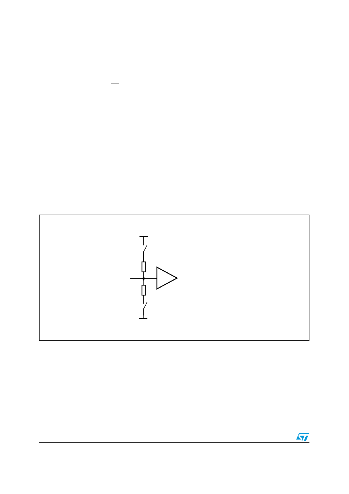
3.1 Status/method pin
This pin is either input or output depending on the operating conditions. It is input before the
start of the detection process (used to set the detection method) and is output at the end of
the detection process (it outputs the result of the detection). The application designer should
program the application controller so that it sets the level of this pin (V
detection starts and maintains it during the falling edge of the shutdown signal (when the
value is internally latched). The STUSBCD01B then outputs the detection result (at the end
of detection) on this pin and therefore the application should read it after the maximum
detection time has passed (see parameters T
STUSBCD01B datasheet). The output structure is not a standard CMOS output but consists
of a weak pull-up or a weak pull-down (~10 kΩ) connected to the pin depending on the
detection result as shown in figure 2.
are standard VIO referred CMOS inputs, the remaining pins
or GND) before the
IO
VBUS_DET_CS
and T
VBUS_DET_DC
on the
Figure 2. Status/method pin I/O
STATUS/
STATUS/
METHOD
METHOD
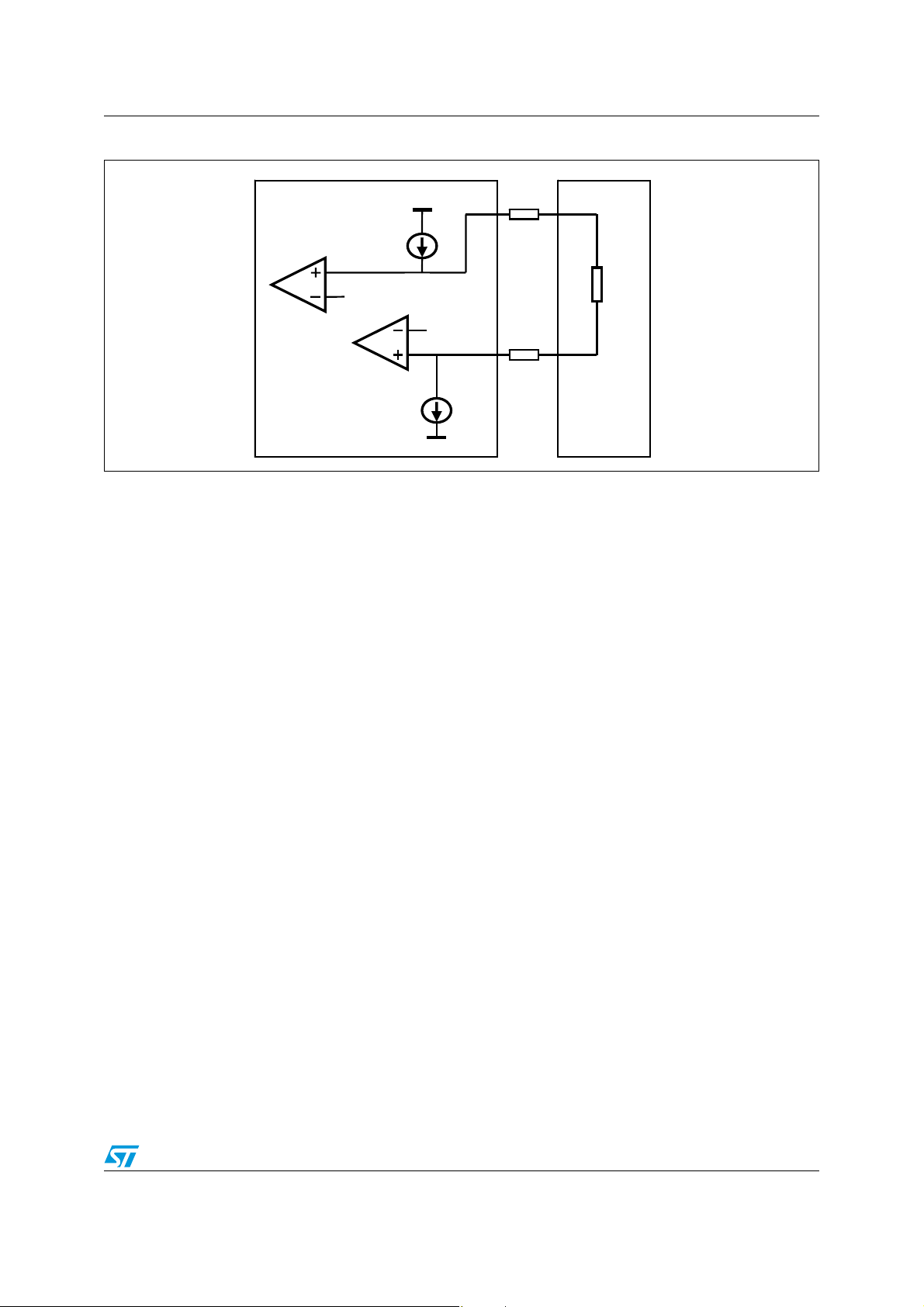
3.2 Detect pin
This pin is an open-drain output which can be used as a V
detection result. It is always enabled in hardware detection mode, while in software
detection mode it is enabled/disabled by the OE
open-drain structure (see Figure 3) uses a PMOS transistor to pull the pin high (V
the detection is successful, otherwise an internal pull-down resistor (~ 300 kΩ) keeps the
output low.
V
V
IO
IO
Closed at detection end if
Closed at detection end if
charger detected
charger detected
Closed at detection end if
Closed at detection end if
charger not detected
charger not detected
GND
GND
(active low) digital input. When enabled, the
referred signal for the
BAT
BAT
) when
6/17 Doc ID 15283 Rev 1
Page 7

AN2865 Interface and control pins
Figure 3. Detect pin output
V
V
BAT
BAT
DETECT
DETECT
GND
GND
3.3 Default method pin
This pin is a V
referred digital input. It is used to choose the detection method in
BAT
hardware detection mode. Its level is ignored in software detection mode. It has to be driven
high for the current sink method, low for the dedicated method.
Note: This pin must never be left floating to avoid increased power consumption.
Doc ID 15283 Rev 1 7/17
Page 8

Current sink detection method AN2865
4 Current sink detection method
The STUSBCD01B's current sink detection method is suitable to detect both dedicated USB
chargers (e.g. wall chargers) and charging host ports and distinguish them from standard
USB host ports. See figure 4 for a simplified schematic description of these devices.
A dedicated charger typically shorts the USB DP/DM lines with a resistance not greater than
200 Ω, while standard USB host ports have pull-down resistors connected to DP and DM
(14.25 - 24.80 kΩ).
A charging host port is normally not distinguishable from standard host ports but if it detects
that an external device connected to its DP/DM lines is attempting to perform a detection,
then it simulates a short between DP/DM, applying a voltage source to DM
(V
DM_SRC
Figure 4. USB ports
= 0.5 - 0.7 V) and a current sink to DP (I
DP_SINK
= 50 - 150 µA).
Dedicated
Dedicated
Charging Port
Charging Port
DP
DP
DM
DM
After a stable V
R
R
DCHG_DAT
DCHG_DAT
Max
Max
200Ω
200Ω
voltage has been detected, if the STUSBCD01B is enabled, the state
BUS
Standard Host
Standard Host
DP
DP
DM
DM
Port
Port
R
R
PD
PD
R
R
PD
PD
DP
DP
DM
DM
Charging Host
Charging Host
R
R
PD
PD
R
R
PD
PD
machine starts the detection procedure which consists of the following steps:
– Phase 1: a current sink is connected to the DM pin (I
DAT_SINK
– Phase 2: 5 ms (min) after DM current sink is connected, a voltage source
(V
DAT_SRC
= 0.615 - 0.7 V) is applied to the DP pin and maintained for at least 100
ms;
– When the detection finishes, both the current sink and the voltage source are
disconnected from the DP/DM pins. If the detection is successful, 40 ms (min.) after
the end of the detection process, the detect and/or Status/Method outputs are pulled
high.
Port
Port
V
V
DAT_REF
DAT_REF
I
I
DP_SINK
DP_SINK
V
V
DM_SRC
DM_SRC
= 50 - 100 µA);
The detection process can be interrupted if one of the following conditions is satisfied:
–V
voltage goes low;
BUS
– Shutdown input is pulled high (only in SW detection mode);
– Voltage levels on the DP/DM pins are different than expected.
The detection is successful if the DM pin is low during phase 1 and it goes high for at least
20 ms during phase 2.
8/17 Doc ID 15283 Rev 1
Page 9

AN2865 Current sink detection method
The DM check during phase 1 is needed to ensure that PS2 to USB adapters, pulling the
DM line high, are not recognized as chargers. If a PS2 port is recognized as a charger, the
high current drawn during the charging process could damage old PC motherboards which
is why the detection is stopped if the DM line is high during this phase.
On the other hand, if DM is low during phase 1, phase 2 is entered. If a dedicated charging
port is connected to the DP/DM lines, the voltage source connected to the DP line pulls the
DM line over the V
DAT_REF
threshold because of the short-circuit between DP and DM inside
the charging port. The same happens when a charging host port is connected. After
detecting the V
DAT_SRC
source to the DM line which exceeds the V
voltage on the DP line, the charging host port connects a voltage
DAT_REF
threshold.
Both ports allow the detection to be successful.
On the other hand, if a standard host port is connected to the DP-DM lines, the DM voltage
during phase 2 is always low because of the pull-down resistor connected to it. This causes
the detection to fail.
Figure 5. STUSBCD01B current sink method applied to a dedicated charger
Phase 1
Phase 1
STUSBCD01
STUSBCD01
V
V
V
V
LOW
LOW
DAT_SRC
DAT_SRC
DAT_REF
DAT_REF
LOW
LOW
DP
DP
DM
DM
R1
R1
R2
R2
I = 0
I = 0
DCHG_DAT
DCHG_DAT
R
R
Phase 2
Phase 2
STUSBCD01
STUSBCD01
V
V
V
V
HIGH
HIGH
DAT_SRC
DAT_SRC
DAT_REF
DAT_REF
HIGH
HIGH
DP
DP
DM
DM
R1
R1
R2
R2
R
R
DCHG_DAT
DCHG_DAT
I =
I =
I
I
DAT_SINK
DAT_SINK
I
I
DAT_SINK
DAT_SINK
I
I
DAT_SINK
Dedicated
Dedicated
Charger
Charger
The maximum value of R
V
DAT_SRC
V
DAT_REF
minus the voltage drop on the series R1+R2+ R
. The worst-case conditions are obtained using the minimum value of V
DCHG_DAT
recognized as a charger can be easily calculated:
and (R1+R2) and the maximum value for V
DAT_SINK
DAT_REF
and I
DCHG_DAT
DAT_SINK
Dedicated
Dedicated
Charger
Charger
must not go below
:
DAT_SRC
Equation 1
V
DAT_SRC(min)
- I
DAT_SINK(max)
(R1+R2+R
DCHG_DAT
) > V
DAT_REF(max)
Therefore,
Equation 2
R
DCHG_DAT
< [(V
DAT_SRC(min)
- V
DAT_REF(max)
)/I
DAT_SINK(max)
]- (R1+R2)
(max)
Considering 1% tolerance for R1 and R2 (470 Ω nominal) and min/max values taken from
the USB battery charging specification and the STUSBCD01B datasheet, we obtain:
Equation 3
R
DCHG_DAT
< [(0.615-0.34)/(100*10-6)]-(470*2*1.01) = 1800.6 Ω
Doc ID 15283 Rev 1 9/17
Page 10

Current sink detection method AN2865
This shows that even by adding R1 and R2 series resistors there is still enough margin over
the dedicated charger’s detection (R
In the case of charging host ports, V
DCHG_DAT(max)
DM_SRC
= 200 Ω according to USB specs).
is applied directly to R2 as shown in figure 6.
The maximum value for R2 which allows a charging host port to be recognized as the
charger after it applies V
DM_SRC
and I
DP_SINK
to DM and DP can be calculated as follows:
Equation 4
V
DM_SRC(min)
- R2*(I
DAT_SRC(max)
) > V
DAT_REF(max)
Equation 5
R2 < (V
DM_SRC(min)
- V
DAT_REF(max)
)/I
DAT_SINK(max)
That is:
Equation 6
R2 < (0.5-0.34)/(100*10-6) = 1600 Ω
A value of 470 Ω (1%) is therefore well within limits.
Figure 6. STUSBCD01B current sink method applied to a charging host port
STUSBCD01
STUSBCD01
I
I
DAT_SINK
DAT_SINK
V
V
DAT_SRC
DAT_SRC
V
V
DAT_REF
DAT_REF
DP
DP
DM
DM
R1
R1
R2
R2
Charging Host Port
Charging Host Port
R
R
PD
PD
I
I
DP_SINK
DP_SINK
R
R
PD
PD
V
V
V
V
DAT_REF
DAT_REF
DM_SRC
DM_SRC
10/17 Doc ID 15283 Rev 1
Page 11

AN2865 Dedicated charger detection method
5 Dedicated charger detection method
The STUSBCD01B's current sink detection method is not able to distinguish between a
charging host port and a dedicated charger. If the result of the current sink method detection
is positive, the user may want to perform a new detection to understand what kind of charger
is connected. The dedicated charger detection method is successful only if a dedicated
charger is connected to the DP/DM lines. If the STUSBCD01B is enabled and configured to
use this method, after a stable V
following operations:
– Phase 1: a current source (I
the end of this phase (100 ms min), both DP and DM lines are high, the detection
proceeds to phase 2;
– Phase 2: I
DAT_SINK
current sink (same as in current sink method, 50 - 100 µA) is
connected to the DM line for at least 40 ms.
If at the end of phase 2 both DP and DM are low, the detection is successful and detect
and/or Status/Method outputs are pulled high.
If a standard host port is connected, the dedicated charger detection method stops at phase
1 because the pull-down resistor on the host side pulls the DM line low.
The case of a charging host port (CHP) is a little bit more complex. During phase 1, the CHP
connects the I
I
DCH_SRC
and therefore pulls the DP line low, causing the detection to fail (the voltage drop
DP_SINK
current sink to the DP line. This current sink is stronger than
over the R1 resistor is negligible because of the low current flowing in it). If for some reason
the voltage drop over I
DP_SINK
STUSBCD01B's DP pin exceeds the V
phase 2 which fails because the DM line is driven high by V
HCP (the DM line is expected to be low during phase 2). This scenario is shown in figure 7.
voltage is detected, the state machine starts the
BUS
DCH_SRC
= 15 - 30 µA) is connected to the DP line. If at
or R1 is higher than expected and the voltage at the
DAT_REF
threshold, the state machine proceeds to
DM_SRC
connected inside the
Figure 7. STUSBCD01B dedicated charger detection method applied to a charging host port
1.8 V
STUSBCD01
STUSBCD01
I
I
DCH_SRC
DCH_SRC
V
V
THDPL
THDPL
I
I
DAT_SINK
DAT_SINK
(Connected
(Connected
only during
only during
phase 2)
phase 2)
1.8 V
V
V
DAT_REF
DAT_REF
DP
DP
DM
DM
R1
R1
R2
R2
Charging Host Port
Charging Host Port
R
R
PD
PD
I
I
DP_SINK
DP_SINK
R
R
PD
PD
V
V
V
V
DAT_REF
DAT_REF
DM_SRC
DM_SRC
The maximum value for the R2 resistor can be easily calculated:
Equation 7
V
DM_SRC(min)
- R2*(I
DAT_SINK(max)
) > V
DAT_REF( max)
Doc ID 15283 Rev 1 11/17
Page 12

Dedicated charger detection method AN2865
Equation 8
R2 < (V
DM_SRC(min)
- V
DAT_REF(max)
)/(I
DAT_SINK(max)
)
Equation 9
R2
= (0.5 - 0.34)/(100*10-6) = 1600 Ω
(max)
This result is consistent with the value in Equation 6 on page 10.
In the case of a dedicated charger, the maximum DP/DM short resistance which is detected
as a charger can be calculated as follows. During phase 1, the value is not significant as
I
DAT_SINK
is off, therefore the resistor series (R1 + R
DCHG_DAT
+ R2) is connected to a high
voltage on the DP side and is floating on the DM side. The voltage is high on both sides.
During phase one, the DM voltage is equal to the voltage drop over I
DAT_SINK
. This current
sink is designed to have a maximum voltage drop, while in operation, of 150 mV. This value
is lower than V
DAT_REF
so it is not critical. In order for the detection to be successful, the DP
line must also be low during phase 2:
Equation 10
V
IDAT_SINK(max)
+ I
DAT_SINK(max)
*[R
DCHG_DAT
+ (R1 + R2)(max)] < V
THDPL(min)
Equation 11
R
DCHG_DAT
< [(V
THDPL(min)
- V
IDAT_SINK(max)
)/I
DAT_SINK(max)
] - (R1 + R2)
(max)
Considering 1% tolerance for R1 and R2 (470 Ω nominal) we obtain:
Equation 12
R
DCHG_DAT(max)
= [0.6 - 0.15)/ (100*10-6)] - (470*2*1.01) = 3550.6 Ω
This result is higher than the one found in Equation 3 on page 9 for the current sink method.
The actual result is even higher than this because in the above calculation we have
considered a maximum value for the current flowing in the resistors higher than the real one.
In fact, having two different current sources on the same branch causes the current to be set
to the value of the weak current source (max 30 µA).
This shows that both methods are quite robust and there is sufficient margin in the choice of
the R1 and R2 resistor values.
12/17 Doc ID 15283 Rev 1
Page 13
AN2865 Dedicated charger detection method
Figure 8. STUSBCD01B dedicated charger detection method applied to a dedicated charger
1.8V
STUSBCD01
STUSBCD01
I
I
DCH_SRC
DCH_SRC
V
V
THDPL
THDPL
I
I
(Connected only
(Connected only
during phase 2)
during phase 2)
1.8V
DAT_SINK
DAT_SINK
V
V
DAT_REF
DAT_REF
DP
DP
DM
DM
R1
R1
R2
R2
DCHG_DAT
DCHG_DAT
R
R
Dedicated
Dedicated
Charger
Charger
Doc ID 15283 Rev 1 13/17
Page 14

Software detection and hardware detection AN2865
6 Software detection and hardware detection
If the battery voltage is not high enough to wake up the application controller but is higher
than 2.2 V, the STUSBCD01B can perform an automatic detection to allow the user to start
charging the battery and make its voltage reach a value which will wake up the ASIC. This
automatic detection is called hardware detection while the ASIC controlled detection is
referred to as software detection.
When the ASIC wakes up, the result of the hardware detection is available until the
STUSBCD01B is reset.
The hardware detection mode is automatically entered when the V
In this mode of operation all V
using the default method pin as described in Table 1 on page 5.
As in the software detection mode, the start of the detection process is triggered by the
V
voltage going high. If the detection fails but the V
BUS
detection is performed once per second in an infinite loop as shown in the simplified
flowchart in figure 9. This periodic detection is stopped only if:
– the detection result is positive;
–the V
–the V
Figure 9. HW/SW detection flowchart
V
V
BUS
BUS
HIGH
HIGH
Timer expired
Timer expired
Or V
Or V
voltage drops under the V
BUS
voltage goes high.
IO
goes
goes
Yes
Yes
No
No
high?
high?
IO
IO
voltage is not available.
referred inputs are ignored and the detection method is set
IO
voltage is still present, a new
BUS
threshold;
SW
SW
detection
detection
Is V
High?
Is V
High?
IO
IO
HW
HW
detection
detection
No
No
TH_VBUS
Yes
Yes
IO
End
End
(*)
Start
Start
1s timer
1s timer
Yes
Yes
Is DET
Is DET
High?
High?
End
End
(*)
Yes
Yes
(*)
(*)
DET = Detect. High if charger detected
DET = Detect. High if charger detected
14/17 Doc ID 15283 Rev 1
Page 15

AN2865 References
7 References
– STUSBCD01B datasheet
– USB battery charging draft specification rel.1.1.
Doc ID 15283 Rev 1 15/17
Page 16

Revision history AN2865
8 Revision history
Table 2. Document revision history
Date Revision Changes
21-Sep-2009 1 Initial release.
16/17 Doc ID 15283 Rev 1
Page 17

AN2865
Please Read Carefully:
Information in this document is provided solely in connection with ST products. STMicroelectronics NV and its subsidiaries (“ST”) reserve the
right to make changes, corrections, modifications or improvements, to this document, and the products and services described herein at any
time, without notice.
All ST products are sold pursuant to ST’s terms and conditions of sale.
Purchasers are solely responsible for the choice, selection and use of the ST products and services described herein, and ST assumes no
liability whatsoever relating to the choice, selection or use of the ST products and services described herein.
No license, express or implied, by estoppel or otherwise, to any intellectual property rights is granted under this document. If any part of this
document refers to any third party products or services it shall not be deemed a license grant by ST for the use of such third party products
or services, or any intellectual property contained therein or considered as a warranty covering the use in any manner whatsoever of such
third party products or services or any intellectual property contained therein.
UNLESS OTHERWISE SET FORTH IN ST’S TERMS AND CONDITIONS OF SALE ST DISCLAIMS ANY EXPRESS OR IMPLIED
WARRANTY WITH RESPECT TO THE USE AND/OR SALE OF ST PRODUCTS INCLUDING WITHOUT LIMITATION IMPLIED
WARRANTIES OF MERCHANTABILITY, FITNESS FOR A PARTICULAR PURPOSE (AND THEIR EQUIVALENTS UNDER THE LAWS
OF ANY JURISDICTION), OR INFRINGEMENT OF ANY PATENT, COPYRIGHT OR OTHER INTELLECTUAL PROPERTY RIGHT.
UNLESS EXPRESSLY APPROVED IN WRITING BY AN AUTHORIZED ST REPRESENTATIVE, ST PRODUCTS ARE NOT
RECOMMENDED, AUTHORIZED OR WARRANTED FOR USE IN MILITARY, AIR CRAFT, SPACE, LIFE SAVING, OR LIFE SUSTAINING
APPLICATIONS, NOR IN PRODUCTS OR SYSTEMS WHERE FAILURE OR MALFUNCTION MAY RESULT IN PERSONAL INJURY,
DEATH, OR SEVERE PROPERTY OR ENVIRONMENTAL DAMAGE. ST PRODUCTS WHICH ARE NOT SPECIFIED AS "AUTOMOTIVE
GRADE" MAY ONLY BE USED IN AUTOMOTIVE APPLICATIONS AT USER’S OWN RISK.
Resale of ST products with provisions different from the statements and/or technical features set forth in this document shall immediately void
any warranty granted by ST for the ST product or service described herein and shall not create or extend in any manner whatsoever, any
liability of ST.
ST and the ST logo are trademarks or registered trademarks of ST in various countries.
Information in this document supersedes and replaces all information previously supplied.
The ST logo is a registered trademark of STMicroelectronics. All other names are the property of their respective owners.
© 2009 STMicroelectronics - All rights reserved
STMicroelectronics group of companies
Australia - Belgium - Brazil - Canada - China - Czech Republic - Finland - France - Germany - Hong Kong - India - Israel - Italy - Japan -
Malaysia - Malta - Morocco - Philippines - Singapore - Spain - Sweden - Switzerland - United Kingdom - United States of America
www.st.com
Doc ID 15283 Rev 1 17/17
 Loading...