

Page 1

AN2860
Application note
EMC guidelines
for STM8 microcontrollers
Introduction
To meet the demand for higher performance, complexity and cost reduction, the
semiconductor industry develops microcontrollers with both high density design technology
and higher clock frequencies. This has intrinsically increased the potential noise emission
and noise sensitivity.
Therefore, application developers must now apply electromagnetic compatibility (EMC)
“hardening” techniques in the design of hardware, PCB layout, firmware and at system level.
This application note is intended for application designers who need to reach the optimum
level of EMC performance. It gives an overview of microcontroller EMC features and
compliance standards.
This document focuses on STM8 features, behaviors and on the differences between the
STM8 family members. For general information on EMC for ST microcontrollers, refer to the
“EMC design guide for ST microcontrollers” application note (AN1709).
General recommendations for STM8 devices are summarized in the “Getting started”
application notes. These documents also provide basic EMC recommendations.
Related documents
AN1015: Software techniques for improving microcontroller EMC performance
AN1709: EMC design guide for ST microcontrollers
AN2752: Getting started with the STM8S and STM8A
AN2867: Oscillator design guide for ST microcontrollers
AN3029: Getting started with the STM8L
AN3181: Guidelines for obtaining IEC60335 Class B certification on STM8 family
RM0013: STM8L101xx microcontroller family reference manual
RM0016: STM8S and STM8A microcontroller family reference manual
RM0031: STM8L15x microcontroller family reference manual
August 2011 Doc ID 15267 Rev 4 1/16
www.st.com
Page 2

Contents AN2860
Contents
1 STM8 and EMC robustness . . . . . . . . . . . . . . . . . . . . . . . . . . . . . . . . . . . 5
2 Application design robustness . . . . . . . . . . . . . . . . . . . . . . . . . . . . . . . . 6
2.1 Power supply . . . . . . . . . . . . . . . . . . . . . . . . . . . . . . . . . . . . . . . . . . . . . . . 6
3 PCB layout recommendations . . . . . . . . . . . . . . . . . . . . . . . . . . . . . . . . . 9
3.1 Two-layer board . . . . . . . . . . . . . . . . . . . . . . . . . . . . . . . . . . . . . . . . . . . . . 9
3.2 Single layer board . . . . . . . . . . . . . . . . . . . . . . . . . . . . . . . . . . . . . . . . . . 12
4 EMC characteristics . . . . . . . . . . . . . . . . . . . . . . . . . . . . . . . . . . . . . . . . 12
5 Software recommendations . . . . . . . . . . . . . . . . . . . . . . . . . . . . . . . . . . 13
5.1 Critical bytes and opcode technique . . . . . . . . . . . . . . . . . . . . . . . . . . . . 13
5.2 Reset sources . . . . . . . . . . . . . . . . . . . . . . . . . . . . . . . . . . . . . . . . . . . . . 13
6 Revision history . . . . . . . . . . . . . . . . . . . . . . . . . . . . . . . . . . . . . . . . . . . 15
2/16 Doc ID 15267 Rev 4
Page 3

AN2860 List of tables
List of tables
Table 1. Document revision history . . . . . . . . . . . . . . . . . . . . . . . . . . . . . . . . . . . . . . . . . . . . . . . . . 15
Doc ID 15267 Rev 4 3/16
Page 4

List of figures AN2860
List of figures
Figure 1. STM8S power connections . . . . . . . . . . . . . . . . . . . . . . . . . . . . . . . . . . . . . . . . . . . . . . . . . . 7
Figure 2. STM8L power connections . . . . . . . . . . . . . . . . . . . . . . . . . . . . . . . . . . . . . . . . . . . . . . . . . . 8
Figure 3. Top view of a 64-pin package layout. . . . . . . . . . . . . . . . . . . . . . . . . . . . . . . . . . . . . . . . . . 10
Figure 4. Bottom view of a 64-pin package layout . . . . . . . . . . . . . . . . . . . . . . . . . . . . . . . . . . . . . . . 11
Figure 5. Top view of a 32-pin package layout . . . . . . . . . . . . . . . . . . . . . . . . . . . . . . . . . . . . . . . . . 12
4/16 Doc ID 15267 Rev 4
Page 5

AN2860 STM8 and EMC robustness
1 STM8 and EMC robustness
Most STM8 product family applications require a high level of EMC robustness. The
considered level of robustness is closely linked to application purposes. The different levels
of robustness are defined by international EMC class standards together with criteria for
testing and measurement techniques used to classify these levels.
One of the pivotal IEC (international electrotechnical commission) standards is the IEC
61000 standard which defines the following robustness classes:
– Class A: No failure detected
– Class B: Failure detected but self-recovery after disturbance
– Class C: An external user action needed to recover normal functionality
– Class D: Normal functionality cannot be recovered
Note: IEC is a world wide recognized authority on international standards for a vast range of safety
issues concerning electrical, electronic and related technologies. It is important to note that
there are several other recognized bodies concerning electronic safety standards besides
IEC, such as VDE in Germany, IET in the United Kingdom and the IEEE in the United
States.
Class B has a different meaning from that used in the IEC 61000 standard as it means in
this case that the application is classified from a safety point of view. See the IEC 60335
standard in the AN3181: Guidelines for obtaining IEC60335 Class B certification on STM8
family.
EMC robustness is a complex result of several factors and it depends on the component
design. However, a very good EMC robustness of any component may be degraded by its
incorrect position into the PCB design or by an incorrect hardware project. These factors are
discussed in more details in the next chapters.
Another important factor is the software solution which can significantly improve the
robustness of the application by a proper software reaction when any disturbance is
detected, which is fundamental, especially for Class-B compliant applications.
In most cases, it is possible to recover the application internally even if the user is not aware
of the internal issues. It is also possible to predict an imminent error state by using some
efficient techniques capable of testing permanently if both the MCU and the application work
properly.
Note: These techniques are further described in the following documents: application notes
AN1015 (Software techniques for improving microcontroller EMC performance) and
AN3181 (Guidelines for obtaining IEC60335 Class B certification on STM8 family)
Doc ID 15267 Rev 4 5/16
Page 6

Application design robustness AN2860
2 Application design robustness
Even though the STM8 has been designed for a high level of EMC robustness, the user
should be aware that the modern high-density CMOS technology used for the STM8 design
is commonly and naturally noise sensitive.
This factor must be taken into account in users’ projects: this is important to avoid steps
which could lead to a degradation of the EMC robustness, especially in applications working
in an “aggressive” environment.
Some specific requirements and recommendations are given in the rest of this chapter.
2.1 Power supply
The STM8S and STM8A product families are designed for standard applications in the
3.3 V to 5 V (+/-10%) supply voltage range.
All power pins must be connected: V
The V
pin is the regulator output used on STM8S and STM8A devices only. It provides
CAP
DD/VSS
, V
DDA/VSSA
, V
DDIOx/VSSIOx
.
the 1.8 V supply to the core and the peripherals. This pin must be decoupled with a
capacitance of at least 470 nF. If the capacitance of an applied capacitor drops under this
level due to temperature or lifetime changes or if a wrong capacitor value is connected, the
reset pin can toggle with a period of about 100 ms. To satisfy this minimum limit value, it is
recommended to use a capacitor with a higher capacitance (about 680 nF), taking into
account possible changes of this capacitance due to environment conditions and the period
of utilization.
The V
pin is used in the STM8L152xx devices to provide a voltage from 2.5 V to 3.6 V to
LCD
the built-in LCD drivers. An external capacitor from 0.1 to 2 µF must be connected to this pin
to stabilize the LCD reference voltage.
For products with separated V
strongly recommended to decouple both with a capacitor of 100 nF. V
DD
and V
, it is mandatory to supply both pins and
DDIO1
DDA
and V
DDIO2
, when
present, must also be decoupled with a dedicated 100 nF capacitor.
Power supply connections are shown in the following diagrams.
6/16 Doc ID 15267 Rev 4
Page 7

AN2860 Application design robustness
6$$!
633!
!NALOG
FUNCTIONS
(3),3)
-AIN,OW
POWERREGULATOR
#052!-
&LASHLOGIC
633
!NALOG
INPUTS
!NALOG
POWER
!).
!).
!).N
6#!0
$IGITAL
POWER
)/LOGIC
(3%
6
$$
/3#).
/3#/54
6$$)/I
633)/I
62%&
62%&
!NALOG
REFERENCE
6$$)/ 633)/
/3#
/3#/54
3()%,$).'
BJ
Figure 1. STM8S power connections
).
Doc ID 15267 Rev 4 7/16
Page 8

6$$!
633!
!NALOG
FUNCTIONS
(3),3)
-AIN,OW
POWERREGULATOR
#052!-
&,!3(LOGIC
633
!NALOG
INPUTS
!NALOG
POWER
!).
!).
!).N
$IGITAL
POWER
)/LOGIC
(3%
6
$$
/3#).
/3#/54
6$$)/I
633)/I
62%&
62%&
!NALOG
REFERENCE
,#$
,#$
POWER
6$$)/ 633)/
3()%,$).'
,3%
/3#).
/3#/54
6$$)/ 633)/
/
/3#/54
/3#
/3#/54
6,#$
BJ
Application design robustness AN2860
Figure 2. STM8L power connections
3#).
).
8/16 Doc ID 15267 Rev 4
Page 9

AN2860 PCB layout recommendations
3 PCB layout recommendations
Figure 1 and Figure 2 defines the appropriate bill of materials but, for EMC performance,
special attention must be paid to the layout which defines ground plane, track width and
length, etc.
It is also important to pay special attention to the following tasks:
● The ground plane should be used as a shield below the device
● The power supply planes must be designed around the device towards the other
components, as shown in Figure 3, Figure 4 and Figure 5. The purpose is to separate
the current flow supplying the rest of the application from the CPU power supply plane
● Every supply pin should be decoupled by a ceramic capacitor. The capacitor should be
placed as close as possible to the supply pin and connected to V
as possible.
STM8S and STM8A devices require an additional external capacitor for a voltage regulator
connected through the V
● The correct value of the capacitor is very critical (a min. 470 nF capacitance must be
CAP
pin:
kept in any condition)
● The capacitor should be placed as close as possible to V
CAP
ground plane.
with a path as short
SS
pin and with the shortest
Warning: Special care must be taken on the device EMC robustness
when the application requires the use of an external (HSE)
oscillator (for instance, for permanent asynchronous
communication or time-dependent measuring) and the
internal clock source cannot be used.
A potential risk of EMC robustness degradation can be
minimized by applying the rules described below.
● The ground path between the capacitor-loaded resonator and V
possible.
● It is better to use a resonator with a metal cap which should be connected to Vss
whenever possible.
● An additional shielding structure should surround the area of the crystal resonator and
of the associated components (see Figure 3, Figure 4 and Figure 5)
3.1 Two-layer board
Due to the position of V
pin packages and above.
DDIO2
and V
must be as short as
SS
, a two-layer board design is recommended for 44-
SSIO2
Doc ID 15267 Rev 4 9/16
Page 10

PCB layout recommendations AN2860
VSS
VDD
Crystal
Supplies towards other components
1: RESET
2: OSCIN
3: OSCOUT
4: VSSIO1
5: VSS
6: VCAP
7: VDD
8: VDDIO1
19: VDDA
20: VSSA
39: VSSIO2
40: VDDIO2
ai15361
1
Figure 3. Top view of a 64-pin package layout.
Note: Grey: bottom side
Dark grey: top side
10/16 Doc ID 15267 Rev 4
Page 11

AN2860 PCB layout recommendations
Crystal
ai15362
Figure 4. Bottom view of a 64-pin package layout
Note: Grey: bottom side
Dark grey: top side
Doc ID 15267 Rev 4 11/16
Page 12

EMC characteristics AN2860
VSS
VDD
Supplies towards other components
Crystal
1
1: RESET
2: OSCIN
3: OSCOUT
4: VSS
5: VCAP
6: VDD
7: VDDIO1
9: VDDA
10: VSSA
ai15363B
3.2 Single layer board
For 32-pin package and below, a single layer board can offer a very good level of EMC
performance.
Figure 5. Top view of a 32-pin package layout
4 EMC characteristics
EMC characteristics are specific to each device. Please refer to the Electrical characteristics
section in the product datasheet for any information on these characteristics.
12/16 Doc ID 15267 Rev 4
Page 13

AN2860 Software recommendations
5 Software recommendations
The standard software techniques for improving EMC performance described in the AN1015
application note (“Software techniques for improving microcontroller EMC performance”)
also apply to the STM8 product family.
This section lists the STM8 specificities related to the software techniques referred in the
AN1015. It gives the values dedicated to STM8 products but it is strongly recommended to
read carefully the AN1015 in order to implement safely the software recommendations.
Some other techniques used to test the MCU correct state and to prevent from an
unexpected MCU behavior are described in details in the AN3181 (Guidelines for obtaining
IEC60335 Class B certification on STM8 family). These techniques are used in the
associated firmware.
5.1 Critical bytes and opcode technique
It is recommended to avoid occurrences of the following critical bytes in your code:
● 0x8E: opcode for HALT (instruction used to enter low power modes)
● 0x8F: opcode for WFI (instruction “wait for interrupt”)
● 0x82: opcode for INT (instruction used to jump in interrupt routine only)
● 0x8B: opcode for SWBRK (software breakpoint instruction used to stall the CPU in
debug mode)
These critical bytes can be generated by the linker when computing the address destination
in a branch instruction (JUMP or CALL) in absolute or relative addressing modes. To remove
such occurrences you can simply insert a NOP instruction before the target address. For
further explanation, refer to the AN1015 application note.
To keep a better control of unexpected jumps, it is recommended to fill unused memory
areas with the TRAP opcode (0x83).
Besides, if you want to generate an illegal opcode reset, illegal opcodes can be used, like for
example the following simple ones: 0x05, 0x0B, 0x71 and 0x75.
5.2 Reset sources
Reset sources can be checked in the Reset status register RST_SR. They can be identified
through the Reset status register.
The following reset sources are available for all STM8 devices:
● SWIM reset,
● Illegal opcode reset,
● Independent watchdog reset.
A few additional reset sources are available only on some devices:
● EMC reset,
● Window watchdog reset,
● POR reset,
● BOR threshold reset.
Doc ID 15267 Rev 4 13/16
Page 14

Software recommendations AN2860
For more details on these reset sources and their differences between devices, please refer
to the dedicated STM8 family reference manuals and device datasheets.
14/16 Doc ID 15267 Rev 4
Page 15
AN2860 Revision history
6 Revision history
Table 1. Document revision history
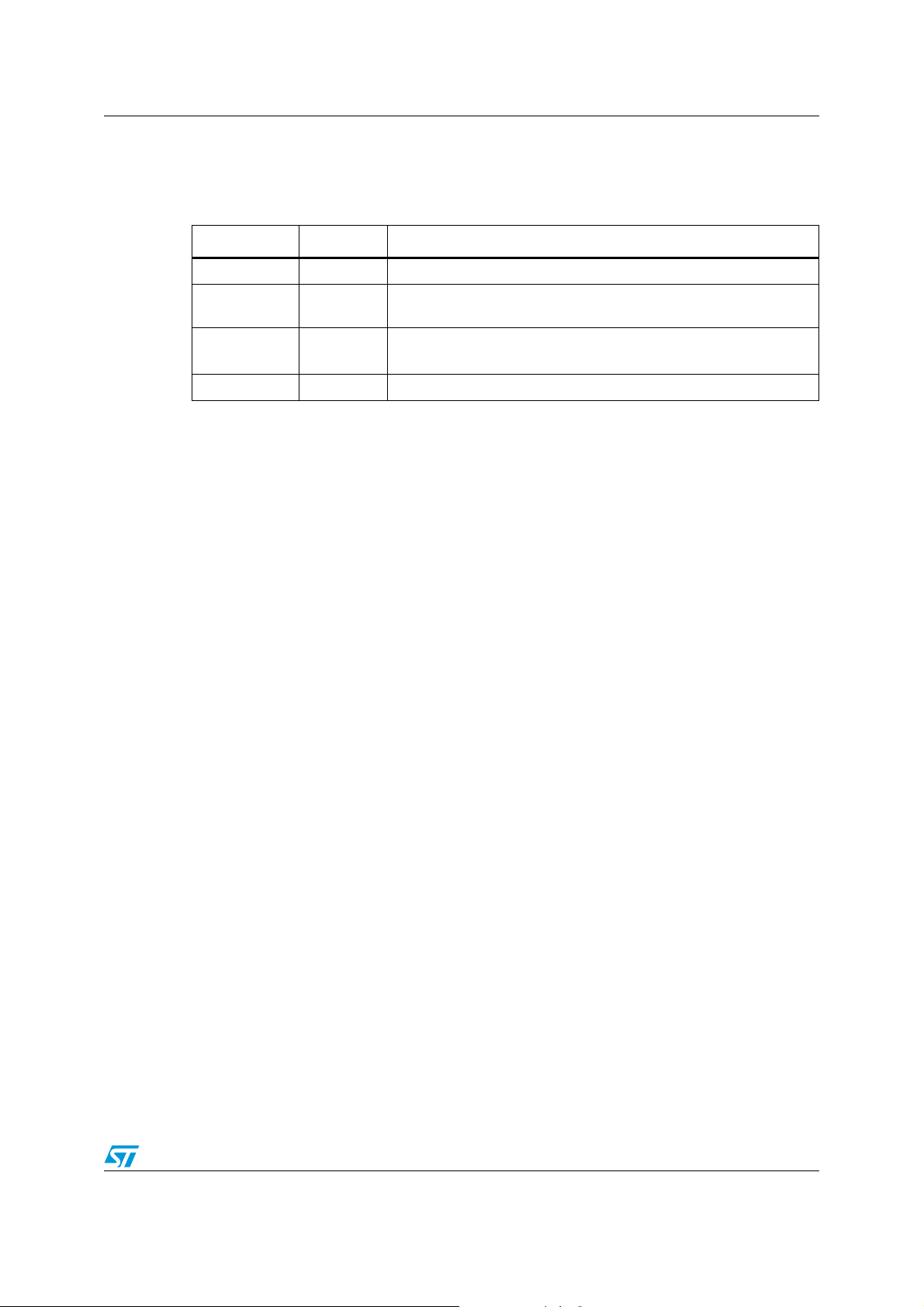
Date Revision Changes
13-Jan-2009 1 Initial release.
27-Jan-2009 2
31-May-2010 3
25-Aug-2011 4 Updated to add references to STM8A devices
Figure 5: Top view of a 32-pin package layout on page 12 modified:
capacitors moved (pins 5 and 7).
Information on STM8A and STM8L family devices added.
Document updated.
Doc ID 15267 Rev 4 15/16
Page 16

AN2860
Please Read Carefully:
Information in this document is provided solely in connection with ST products. STMicroelectronics NV and its subsidiaries (“ST”) reserve the
right to make changes, corrections, modifications or improvements, to this document, and the products and services described herein at any
time, without notice.
All ST products are sold pursuant to ST’s terms and conditions of sale.
Purchasers are solely responsible for the choice, selection and use of the ST products and services described herein, and ST assumes no
liability whatsoever relating to the choice, selection or use of the ST products and services described herein.
No license, express or implied, by estoppel or otherwise, to any intellectual property rights is granted under this document. If any part of this
document refers to any third party products or services it shall not be deemed a license grant by ST for the use of such third party products
or services, or any intellectual property contained therein or considered as a warranty covering the use in any manner whatsoever of such
third party products or services or any intellectual property contained therein.
UNLESS OTHERWISE SET FORTH IN ST’S TERMS AND CONDITIONS OF SALE ST DISCLAIMS ANY EXPRESS OR IMPLIED
WARRANTY WITH RESPECT TO THE USE AND/OR SALE OF ST PRODUCTS INCLUDING WITHOUT LIMITATION IMPLIED
WARRANTIES OF MERCHANTABILITY, FITNESS FOR A PARTICULAR PURPOSE (AND THEIR EQUIVALENTS UNDER THE LAWS
OF ANY JURISDICTION), OR INFRINGEMENT OF ANY PATENT, COPYRIGHT OR OTHER INTELLECTUAL PROPERTY RIGHT.
UNLESS EXPRESSLY APPROVED IN WRITING BY TWO AUTHORIZED ST REPRESENTATIVES, ST PRODUCTS ARE NOT
RECOMMENDED, AUTHORIZED OR WARRANTED FOR USE IN MILITARY, AIR CRAFT, SPACE, LIFE SAVING, OR LIFE SUSTAINING
APPLICATIONS, NOR IN PRODUCTS OR SYSTEMS WHERE FAILURE OR MALFUNCTION MAY RESULT IN PERSONAL INJURY,
DEATH, OR SEVERE PROPERTY OR ENVIRONMENTAL DAMAGE. ST PRODUCTS WHICH ARE NOT SPECIFIED AS "AUTOMOTIVE
GRADE" MAY ONLY BE USED IN AUTOMOTIVE APPLICATIONS AT USER’S OWN RISK.
Resale of ST products with provisions different from the statements and/or technical features set forth in this document shall immediately void
any warranty granted by ST for the ST product or service described herein and shall not create or extend in any manner whatsoever, any
liability of ST.
ST and the ST logo are trademarks or registered trademarks of ST in various countries.
Information in this document supersedes and replaces all information previously supplied.
The ST logo is a registered trademark of STMicroelectronics. All other names are the property of their respective owners.
© 2011 STMicroelectronics - All rights reserved
STMicroelectronics group of companies
Australia - Belgium - Brazil - Canada - China - Czech Republic - Finland - France - Germany - Hong Kong - India - Israel - Italy - Japan -
Malaysia - Malta - Morocco - Philippines - Singapore - Spain - Sweden - Switzerland - United Kingdom - United States of America
www.st.com
16/16 Doc ID 15267 Rev 4
 Loading...