

Page 1
AN2859
Application note
Multiplexed diagnostics of AC switches using two STCC08s
Introduction
The aim of this application note is to present opportunities to reduce the number of input
pins used on a microcontroller unit (MCU) to diagnose failures of several AC switches with
the STCC08. This document deals with the multiplexed diagnostics of two STCC08 and
gives technical recommendations on the implementation of this solution.
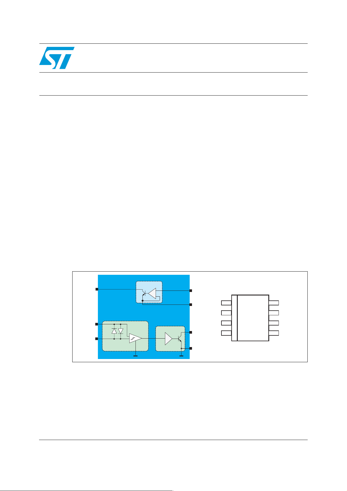
STCC08 overview
The STCC08 has been designed to improve home appliance safety. This new device can
drive an AC switch (Triac, ACST and ACS) with a gate current I
back to the microcontroller unit a signal image of the voltage across the controlled AC switch
(this signal defines the AC switch state). The STCC08 has three functional blocks (see
Figure 1).
■ A "gate driver" block used to drive an AC switch and to interface directly the STCC08 with
the MCU (CMOS compatible)
■ A "power switch signal shaping" block used to measure the AC switch voltage in both AC
line cycles
■ An "AVF driver" block used to give an image of the AC switch voltage to the MCU (digital
information)
up to 10 mA and to send
GT
Figure 1. STCC08 block diagram
G
V
CC
AC
Power switch
signal shaping
Gate driver
+
-
STCC08
STCC08
AVF driver
IN
R
IG
AVF
AVF
GND
GND
IN
AVF
N/C
AC
1
2
3
4
SO -8
8
7
6
5
For more information about the STCC08, please refer to the ST Application note AN2716.
December 2009 Doc ID 15255 Rev 1 1/29
GND
R
IG
G
V
CC
www.st.com
Page 2

Contents AN2859
Contents
1 Multiplexed diagnostics . . . . . . . . . . . . . . . . . . . . . . . . . . . . . . . . . . . . . . 3
1.1 Principle . . . . . . . . . . . . . . . . . . . . . . . . . . . . . . . . . . . . . . . . . . . . . . . . . . . 3
1.2 Failure mode detection of two AC switches . . . . . . . . . . . . . . . . . . . . . . . . 4
1.3 V
2V
STATE
signal reading synchronization . . . . . . . . . . . . . . . . . . . . . . . . . . . . . 9
AVF
level definition . . . . . . . . . . . . . . . . . . . . . . . . . . . . . . . . . . . . . . . 11
3 Resistance settings . . . . . . . . . . . . . . . . . . . . . . . . . . . . . . . . . . . . . . . . . 14
4 Detection windows digital value setting . . . . . . . . . . . . . . . . . . . . . . . . 15
5 Application example . . . . . . . . . . . . . . . . . . . . . . . . . . . . . . . . . . . . . . . . 17
6 Conclusion . . . . . . . . . . . . . . . . . . . . . . . . . . . . . . . . . . . . . . . . . . . . . . . . 18
Appendix A AC switch state deduction . . . . . . . . . . . . . . . . . . . . . . . . . . . . . . . . 19
Appendix B V
signal voltage definition . . . . . . . . . . . . . . . . . . . . . . . . . . . . 21
STATE
Appendix C Resistance settings . . . . . . . . . . . . . . . . . . . . . . . . . . . . . . . . . . . . . . 25
C.1 First case: V
C.2 Second case: V
C.3 Third case: V
1_Min
2_Max
> V
0_Max . . . . . . . . . . . . . . . . . . . . . . . . . . . . . . . . . . . . . . . . . . . . . . 25
> V
2_Min
1_Max . . . . . . . . . . . . . . . . . . . . . . . . . . . . . . . . . . . . . . . . . . . 26
< V
3_Min . . . . . . . . . . . . . . . . . . . . . . . . . . . . . . . . . . . . . . . . . . . . . 27
Revision history . . . . . . . . . . . . . . . . . . . . . . . . . . . . . . . . . . . . . . . . . . . . . . . . . . . . 28
2/29 Doc ID 15255 Rev 1
Page 3
AN2859 Multiplexed diagnostics
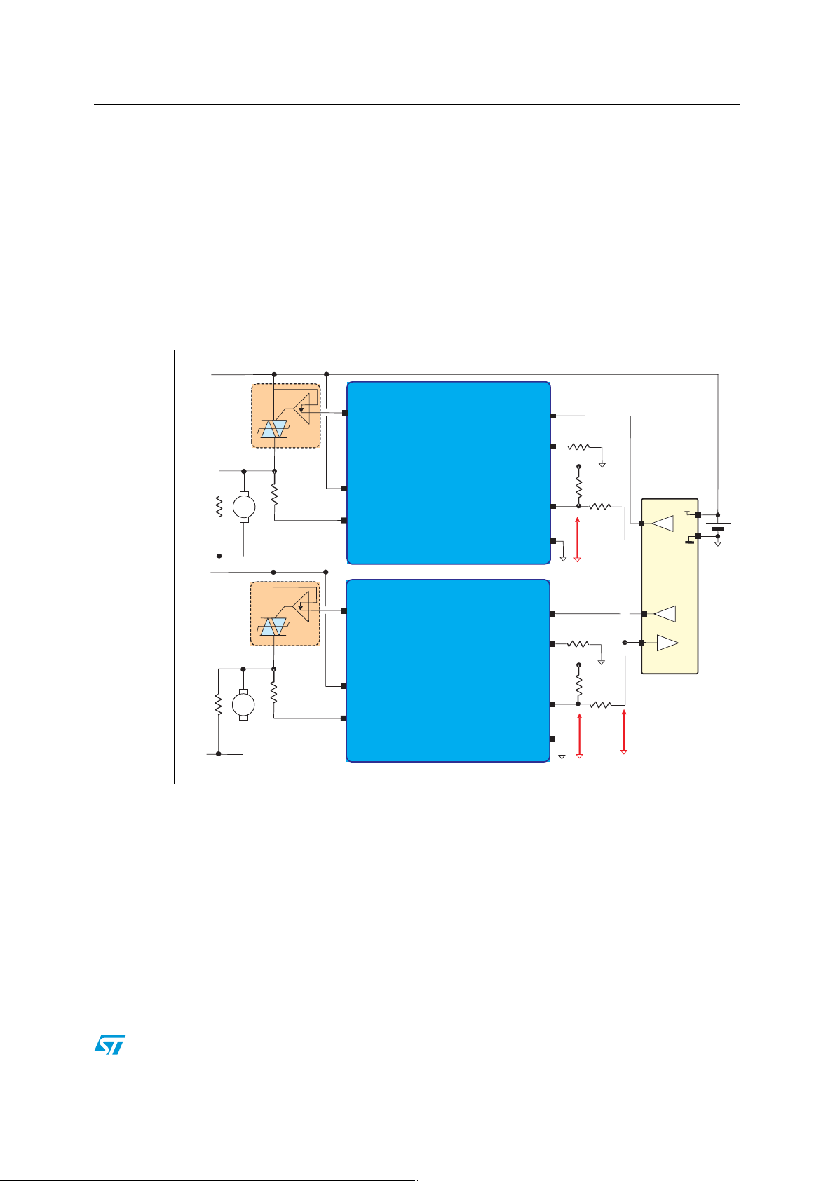
1 Multiplexed diagnostics
1.1 Principle
The multiplexed diagnostic allows the detection of the state of several AC switches
independently using only one MCU input. In this case, an analog/digital converter input
(ADC) of the MCU should be used and must be configured with no pull-up resistor. In this
document, only the multiplexed diagnostic of two STCC08 (STCC08
described (see Figure 2). Note that two output pins of an MCU should be used to control
each STCC08 (IN1 and IN2).
Figure 2. Multiplexed diagnostic schematic of two STCC08
Neutral
R
Shunt
Line
Load2
ACS2
R
AC
V
AC
G
CC
STCC08
2
IN2
R
AVF
AVF
and STCC082) is
1
IG
V
CC
R1
R2
V
AVF2
MCU
V
CC
Neutral
R
Shunt
Line
Load1
ACS1
R
AC
V
AC
G
CC
STCC08
1
To distinguish the state of each AC switch (ACS1 and ACS2) a divider bridge is used.
Resistors R
STCC08 (V
, R2, R3 and R4 are designed to convert the V
1
AVF 1
and V
) into an analog signal (V
AVF 2
STATE
each STCC08 (IN1 and IN2), the MCU is able to identify the state of each AC switch by
analyzing the V
signal (see Section 1.2).
STATE
Note: The STCC08 AVF output is an open collector output. Resistors R
STCC08 AVF output and limit the collector current to 5 mA. For further information, and in
particular, resistor values for R
AC
, R
, and RIG, refer to the ST Application note AN2716.
shunt
IN1
R
IG
V
CC
R3
AVF
AVF
R4
GND
GND
V
digital signal given by each
AVF
AVF1
V
STATE
). Knowing the control state of
and R3 bias the
1
Doc ID 15255 Rev 1 3/29
Page 4
Multiplexed diagnostics AN2859
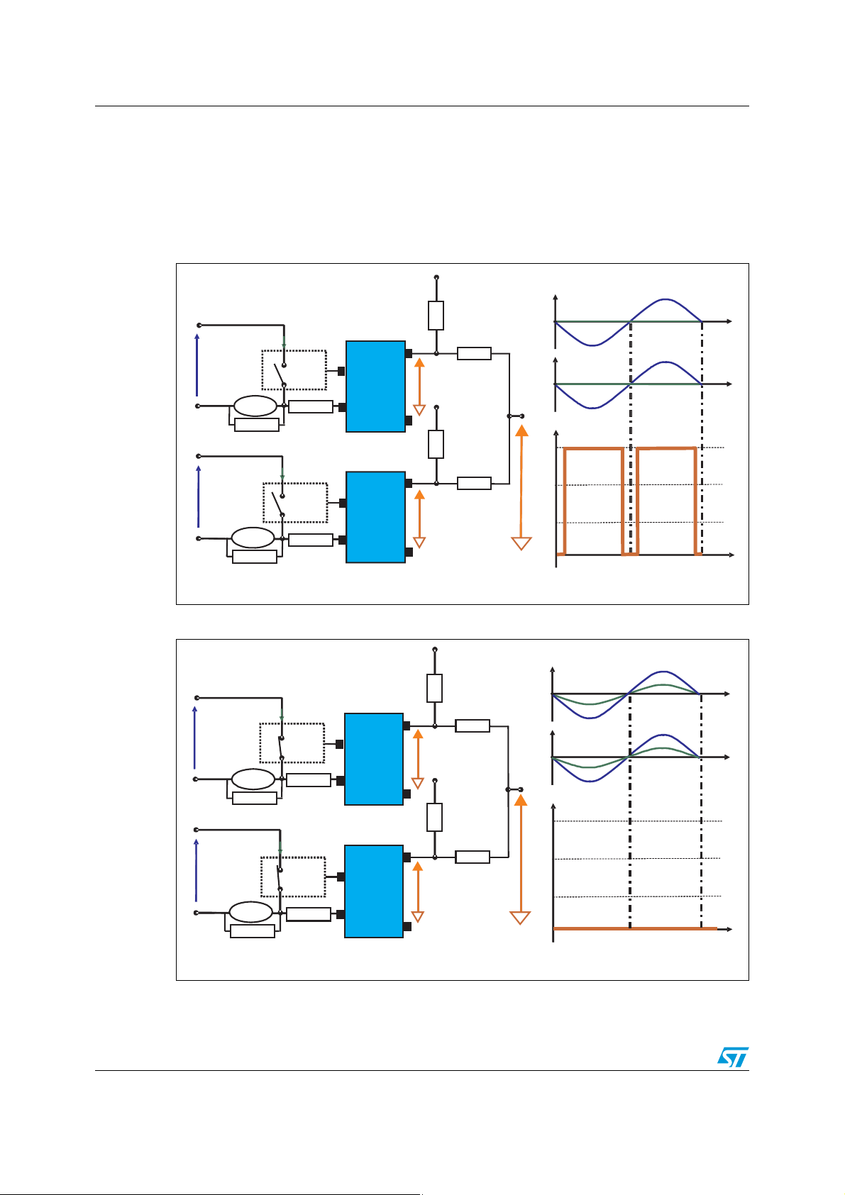
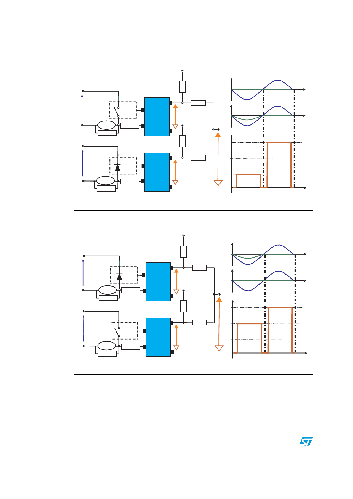
1.2 Failure mode detection of two AC switches
Figure 3 to Figure 12 give the V
V
, V1, V2 and V3 are levels reached by the parameter V
0
signal level according to the state of each AC switch.
STATE
and depends on R1, R2, R3,
STATE
and R4 resitor values.Ta ble 1 shows that we only need four different levels to define the
state of each AC switch.
Figure 3. Case 1: V
VCC/COM
I
Load_2
V
AC
Line
VCC/COM
V
AC
Line
RShunt
Load2
RShunt
Load1
I
Load_1
ACS2
RAC
ACS1
RAC
= V3 (except at each zero crossing of the AC line)
STATE
VCC
VS TATE
V3
V2
V1
V0
I
Load_2
I
Load_1
STCC08
G
AC
STCC08
G
AC
AVF
IN2
AVF
IN1
R1
2
R2
V
AVF2
VCC
R3
1
R4
V
V
AVF1
STAT E
V
AC
V
AC
ACS1 and ACS2 are not in conducting state
Figure 4. Case 2: V
VCC/COM
I
Load_2
V
AC
Line
Load2
RShunt
VCC/COM
V
AC
Line
Load1
RShunt
I
Load_1
ACS2
RAC
ACS1
RAC
STATE
= V
STCC08
G
AC
STCC08
G
AC
0
AVF
IN2
AVF
IN1
VCC
V
AC
R1
2
R2
V
AVF2
I
Load_2
I
Load_1
V
AC
VCC
VSTATE
R3
1
R4
V
V
AVF1
STAT E
V3
V2
V1
V0
ACS1 and ACS2 are in conducting state
4/29 Doc ID 15255 Rev 1
Page 5
AN2859 Multiplexed diagnostics
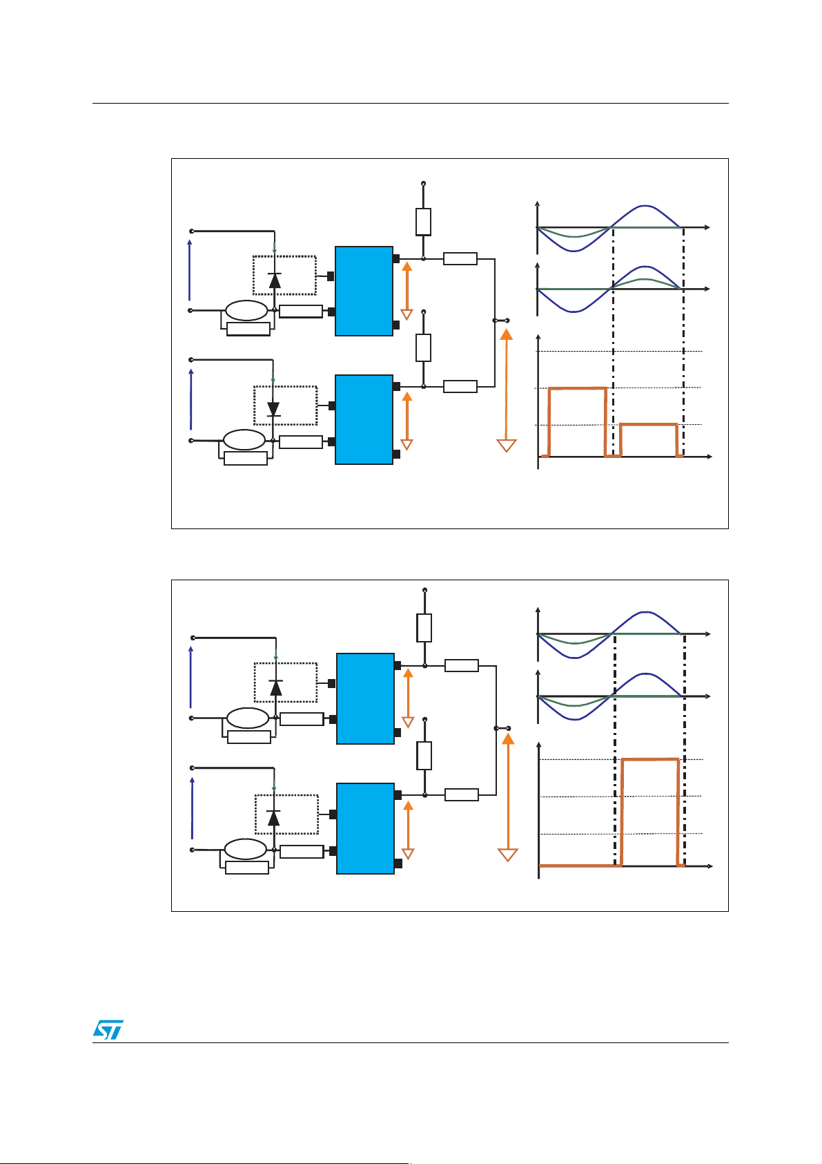
Figure 5. Case 3: V
V /COM
CC
I
Load_2
V
AC
Line
VCC/COM
V
AC
Line
RShunt
Load2
RShunt
Load1
I
Load_1
ACS2
RAC
ACS1
RAC
= V1 (except at each zero crossing of the AC line)
STATE
V
CC
R1
STCC08
G
AC
STCC08
G
AC
2
AVF
IN2
1
AVF
IN1
R2
V
AVF2
V
CC
R3
V3
R4
V2
V
V
AVF1
STATE
V1
V0
ACS1 is in conducting state and ACS2 is not in conducting state
Figure 6. Case 4: V
= V2 (except at each zero crossing of the AC line)
STATE
VCC
V
AVF2
V
AVF1
V
R1
R3
CC
R2
R4
V
STAT E
V3
V2
V1
V0
V /COM
CC
V
AC
Line
Load2
RShunt
V /COM
CC
V
AC
Line
Load1
RShunt
I
Load_2
I
Load_1
ACS2
RAC
ACS1
RAC
STCC08
AVF
G
AC
STCC08
AVF
G
AC
2
IN2
1
IN1
VSTATE
V
STAT E
I
Load_2
I
Load_1
I
Load_2
I
Load_1
V
AC
V
AC
V
AC
V
AC
ACS1 is not in conducting state and ACS2 is in conducting state
Doc ID 15255 Rev 1 5/29
Page 6
Multiplexed diagnostics AN2859
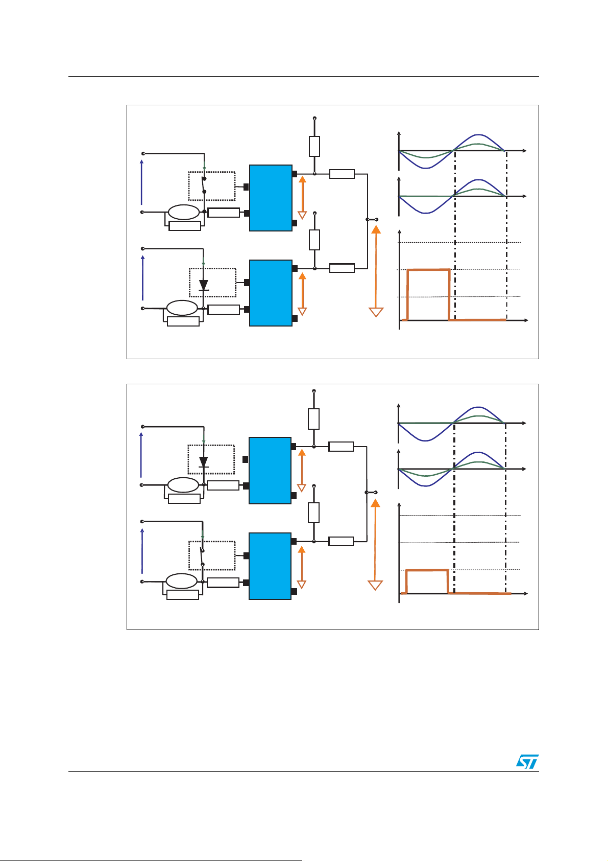
Figure 7. Case 5: V
toggles between V1 and V3 at each AC line cycle
STATE
(except at each zero crossing of the AC line)
V
CC
V /COM
CC
I
Load_2
STCC08
2
R1
R2
AVF
V
AC
Line
Load2
RShunt
V /COM
CC
V
AC
Line
Load1
RShunt
I
Load_1
ACS2
RAC
ACS1
RAC
G
AC
STCC08
AVF
G
AC
IN2
IN1
V
AVF2
V
CC
V
R3
1
R4
V3
V2
V
V
AVF1
STATE
V1
V0
ACS1 is failed in diode mode and ACS2 is not in conducting state
Figure 8. Case 6: V
toggles between V2 and V3 at each AC line cycle
STATE
(except at each zero crossing of the AC line)
V
CC
V
V
AVF2
AVF1
V
R1
R3
CC
R2
R4
V
STAT E
V3
V2
V1
V0
V /COM
CC
V
AC
Line
Load2
RShunt
V /COM
CC
V
AC
Line
Load1
RShunt
I
Load_2
I
Load_1
ACS2
RAC
ACS1
RAC
STCC08
AVF
G
AC
IN2
STCC08
AVF
G
AC
IN1
2
1
STATE
V
STATE
I
Load_2
I
Load_1
I
Load_2
I
Load_1
V
AC
V
AC
V
AC
V
AC
ACS1 is not in conducting state and ACS2 is failed in diode mode
6/29 Doc ID 15255 Rev 1
Page 7
AN2859 Multiplexed diagnostics
Figure 9. Case 7: V
toggles between V1 and V2 at each AC line cycle
STATE
(except at each zero crossing of the AC line)
V
CC
V
V
AVF2
V
AVF1
R1
R3
CC
R2
R4
V
STAT E
V3
V2
V1
V0
V /COM
CC
V
AC
Line
Load2
RShunt
V /COM
CC
V
AC
Line
Load1
RShunt
I
Load_2
I
Load_1
ACS2
RAC
ACS1
RAC
STCC08
AVF
G
AC
STCC08
AVF
G
AC
2
IN2
1
IN1
ACS1 and ACS2 are failed in diode mode not on the same AC line polarities
V
STAT E
I
Load_2
I
Load_1
V
V
AC
AC
Figure 10. Case 8: V
toggles between V0 and V3 at each AC line cycle
STATE
(except at each zero crossing of the AC line)
VCC
V /COMCC
ILoad_2
STCC08
R1
2
R2
ILoad_2
AVF
V
AC
Line
V /COMCC
V
AC
Line
Load2
RShunt
ILoad_1
Load1
RShunt
ACS2
RAC
ACS1
RAC
G
AC
STCC08
AVF
G
AC
IN2
IN1
VAVF2
ILoad_1
VCC
VSTAT E
R3
1
R4
V3
V2
VAVF1
VSTAT E
V1
V0
ACS1 and ACS2 are failed in diode mode on the same AC line polarities
V
AC
V
AC
Doc ID 15255 Rev 1 7/29
Page 8
Multiplexed diagnostics AN2859
Figure 11. Case 9: V
V /COM
CC
I
Load_2
V
AC
Line
Load2
RShunt
V /COM
CC
V
AC
Line
Load1
RShunt
I
ACS2
RAC
Load_1
ACS1
RAC
toggles between V2 and V0 at each AC line cycle
STATE
V
CC
R1
STCC08
2
R2
AVF
G
V
AVF2
V
AC
IN2
CC
R3
STCC08
1
R4
AVF
G
V
AVF1
V
STAT E
AC
IN1
ACS1 is failed in diode mode and ACS2 is failed in short circuit
Figure 12. Case 10: V
V /COM
CC
I
Load_2
V
AC
Line
Load2
RShunt
V /COM
CC
I
V
AC
Line
Load1
RShunt
Load_1
ACS2
RAC
ACS1
RAC
toggles between V1 and V0 at each AC line cycle
STATE
V
CC
R1
STCC08
2
R2
AVF
G
V
AVF2
V
AC
IN2
CC
R3
STCC08
1
R4
AVF
G
V
AVF1
V
STATE
AC
IN1
V3
V2
V1
V0
V3
V2
V1
V0
V
V
STAT E
STATE
I
Load_2
I
Load_1
I
Load_2
I
Load_1
V
AC
V
AC
V
AC
V
AC
ACS1 is failed in shot circuit and ACS2 is failed in diode mode
8/29 Doc ID 15255 Rev 1
Page 9

AN2859 Multiplexed diagnostics
Table 1. Variation of the V
Knowing the control state of each STCC08 (IN1 and IN2) and according to Ta bl e 1, the MCU
is able to detect the AC switch state by analyzing V
states of each ACS according to the V
state of each STCC08. In the case of failure of one of the AC switches, the MCU can place
the application in a safe configuration by switching off an appliance front-end relay.
1.3 V
The STCC08 AVF output signal is an image of the AC switch voltage. This signal toggles
between V
is higher or not than I
electrical variation between ICs may result in the state of the AVF signal of each STCC08
(either V
V
I
V
controlled (IN1 = IN2 = 0) and AC1 and AC2 are not in conducting state the AC1 and AC2
can be interpreted (see Table 1 ) as failed in short circuit if V
(V
signal according to the AC switch states
STATE
ACS1 state ACS2 state V
ON ON V
ON OFF V
OFF ON V
OFF OFF V
signal. Appendix A defines the
signal level (V0, V1, V2 and V3) and the control
STATE
signal reading synchronization
AVF
and zero level (GND) according to whether the STCC08 AC input current (IAC)
CC
or zero level) not changing at exactly the same time. This has an impact on the
CC
signal and on the AC switches state detection (see Figure 13). Note that I
STATE
define respectively the STTCO8 IAC input current for STCC081 and STCC082 to allow
ACT2
signal to toggle between VCC and GND. For example, if the two STCC08 are not
AVF
= V0).
STATE
(see AN2716). In case of multiplexed diagnostics the slight I
ACT
STATE
is read between t0 and t
STATE
STATE
STATE
STATE
STATE
STATE
status
= V
= V
= V
= V
0
1
2
3
ACT1
ACT
and
1
Doc ID 15255 Rev 1 9/29
Page 10

Multiplexed diagnostics AN2859
Figure 13. V
I
ACT2
I
ACT1
-I
ACT1
-I
ACT2
V
CC
V
CC
VSTATE
V
3
V
1
ϕ
t = 0
0
signal variation due to the I
STATE
VLine
I=AC1 IAC2
AVF1 (STCC08_1)
AVF2 (STCC08_2)
Δ
t
t
t
1
2
Detection
parameter dispersion
ACT
t
3
t =
5
t
4
t (s)
t (s)
t (s)
t (s)
1
2 x f
The V
is advised to read the V
should be read between times t2 and t3. To simplify the AC switches detection, it
STATE
signal around the AC line peak voltage to avoid any
AVF
inappropriate interpretation of the AC switches state. Note that when the IN1 and/or IN2
signals are removed, a parasitic detection of the AC switch state exists up to the next AC
load current zero crossing (see AN2716). Anyway to ensure a reliable detection of the AC
switch state when the IN1 and/or IN2 control is removed, the AVF reading should be read 10
ms after the IN1 and/or IN2 control has been removed and at the next peak mains voltage.
Note: It is recommended that the AVF signal be read during several AC line cycles around the AC
line peak voltage.
10/29 Doc ID 15255 Rev 1
Page 11

AN2859 V
V
level definition
STATE
2 V
According to the state of each AC switch, V0, V1, V2 and V3 levels are defined by equations
1, 2, 3 and 4 (see also Appendix B). In this document V
the STCCO8
values of AVF at low level are respectively 0 V and 1 V.
Equation 1
ACS1 and ACS2 are on
Equation 2
ACS1 is on and ACS2 is off
Equation 3
ACS2 is on and ACS1 is off
STATE
=
0
V
=
1
V
=
2
level definition
and STCCO82 AVF output at the low level. The minimum and maximum
1
()
+
+
·RV·RV
4AVF2_L2AVF1_L
RR
42
()
RR·V·RV
++
RRR
++
421
()
RR·V·RV
++
RRR
++
432
21AVF1_L4CC
43AV F2_ L2CC
AVF 1_L
and V
are respectively
AVF 2_L
Equation 4
ACS1 and ACS2 are off
VV =
CC3
The tolerance of the resistors (R
dispersion and the DC power supply characteristics induce a dispersion on V
V
levels (see Ta bl e 2 ).
3
Table 2. Variation of the V
ACS1 state ACS2 state V
ON ON V
ON OFF V
OFF ON V
OFF OFF V
, R2, R3 and R4), the STCC08 output AVF signal electrical
1
signal according to the AC switch states
STATE
< V
0_Min
< V
1_Min
< V
2_Min
3_Max
> V
STATE
STATE
STATE
STATE
STATE
, V1, V2 and
0
status
< V
0_Max
< V
1_Max
< V
2_Max
> V
3_Min
Knowing the previous equations 1, 2, 3 and 4, the resistors standard value and the tolerance
of the resistors, V
x_Max
and V
(x = 0, 1, 2, or 3) values are defined respectively by
x_Min
equations 5, 6, 7, 8, 9, 10, 11 and 12.
Doc ID 15255 Rev 1 11/29
Page 12

V
STATE
level definition AN2859
V
the application. X
resistor tolerance X
V
and V
CC_Min
AVF_L_Min
CC_Max
are respectively the minimum and maximum power supply voltage of
and X
R_Max
R_Max
and X
values are fixed by the STCC08 AVF output electrical dispersion at low level
with:
V
AVF_L_Max
= V
AVF1_L_Max
and
V
AVF_L_Min
= V
AVF1_L_Min
= V
Equation 5
ASC1 is on and ACS2 is on.
⎛
+
⎜
⎝
=
AVF_L_Max0_Max
·VV =
42
⎛
+
⎜
⎝
Equation 6
ASC1 is on and ACS2 is on.
⎛
⎜
⎝
=
AVF_L_Min0_Min
·VV
⎛
⎜
⎝
⎞
+
⎟
42
⎠
⎞
+
⎟
42
⎠
R_Min
R_Min
= V
AVF2_L_Max
AVF2_L_Min
⎞
X·RR
⎟
R_Max
⎠
⎞
X·RR
⎟
42
R_Min
⎠
X·RR
R_Min
X·RR
R_Max
are the tolerances of the resistors. For example, with 5%
are respectively 1.05 and 0.95. V
AVF_L_Max
and
= 1 V
= 0 V
X
R_Max
·V
X
R_Min
=
AVF_L_Max
V0
Equation 7
ASC1 is on and ACS2 is off.
⎞
X·RR·VX·R·V
++
⎟
21
R_Max
⎠
V
1_Max
=
CC_Max
⎛
4
⎛
⎜
⎝
AVF_L_MaxR_Max
++
⎜
⎝
⎞
X·RRR
⎟
421
R_Min
⎠
Equation 8
ASC1 is on and ACS2 is off.
⎞
X·RR·VX·R·V
++
⎟
21
R_Min
⎠
V
1_Min
⎛
CC_Min
4
AVF_L_MinR_Min
=
⎛
⎜
⎝
++
⎜
⎝
⎞
X·RRR
⎟
421
R_Max
⎠
Equation 9
ASC1 is off and ACS2 is on.
⎛
V
2_Max
CC_Max
=
2
⎛
⎜
⎝
AVF_L_MaxR_Max
++
⎜
⎝
⎞
X·RRR
⎟
432
R_Min
⎠
⎞
X·RR·V.XR·V
++
⎟
43
R_Max
⎠
12/29 Doc ID 15255 Rev 1
Page 13

AN2859 V
Equation 10
ASC1 is off and ACS2 is on.
⎞
++
X·RR·VX·R·V
⎟
43
R_Min
⎠
V
2_Min
⎛
CC_Min
2
AVF_L_MinR_Min
=
⎛
⎜
⎝
++
⎜
⎝
⎞
X·RRR
⎟
432
R_Max
⎠
Equation 11
ASC1 is off and ACS2 is off.
VV =
3_Max
CC_Max
Equation 12
ASC1 is off and ACS2 is off.
VV =
3_Min
CC_Min
level definition
STATE
Doc ID 15255 Rev 1 13/29
Page 14

Resistance settings AN2859
3 Resistance settings
Equation 13 shows how to select values for R1 and R3 resistances. I
AVF _Max
is the maximum
current sunk by the STCC08 AVF pin and should be lower than 5 mA.
Equation 13
V·2
RRR ≥==
31
Knowing the R
AVF output electrical dispersion and the DC power supply characteristic, R
CC_Max
I
AVF _Ma x
and R3 resistor standard values, the tolerance of the resistors, the STCC08
1
and R4
2
resistances value should be chosen by using equations 14 , 15 , and 16 (see also
Appendix C).
Equation 14
>⇒
⎧
⎪
⎪
⎪
⎪
⎪
⎪
⎨
⎪
⎪
⎪
⎪
⎪
⎪
⎩
VV
0_Max1_Min
⎡
⎢
⎛
⎜
⎝
>⇒
R
4
⎞
+
⎟
2
AVF_L_Max
⎢
⎠
⎢
⎣
CC_Min
−
⎛
⎜
·V·RR
⎜
⎜
⎝
AVF_L_Max
X
X
R_Max
R_Min
⎛
⎜
·VV
⎜
⎜
⎝
X
X
2
⎞
⎟
⎟
⎟
⎠
R_Max
R_Min
−
V
⎞
⎟
⎟
⎟
⎠
AVF_L_Min
2
⎤
⎥
⎥
⎥
⎦
Equation 15
>⇒
⎧
⎪
⎪
⎪
⎪
⎪
⎪
⎨
⎪
R
⎪
⎪
⎪
⎪
⎪
⎩
VV
1_Max2_Min
2
⎡
⎡
⎢
2
⎢
⎢
⎣
<⇒
4
CC_Min
−
VV·R
AVF_L_Max
⎛
X
⎜
⎜
⎜
X
⎝
CC_Max
R_Max
R_Min
⎤
⎞
⎢
⎥
⎟
−
AVF_L_Max
⎢
⎥
⎟
⎟
⎢
⎥
⎠
⎣
⎦
2
X
X
R_Max
R_Min
⎞
⎟
−
V
⎟
⎟
⎠
⎛
⎜
·V
⎜
⎜
⎝
AVF_L_Min
⎛
⎜
·V·R
⎜
⎜
⎝
X
X
R_Max
R_Min
2
⎞
⎟
V
−
⎟
⎟
⎠
AVF_L_Min
⎤
⎥
⎥
⎥
⎦
Equation 16
>⇒
⎧
⎪
⎪
⎪
⎪
⎪
⎪
⎨
⎪
⎪
⎪
⎪
⎪
⎪
⎩
VV
2_Max3_Min
⎡
⎢
2
⎢
⎣
>⇒
R
4
CC_Min
−
X
R_Min
·V
X
R_Max
CC_MinCC_Max
−
V
AVF_L_Max
·VV·R
X
X
R_Min
R_Max
⎤
⎥
⎥
⎦
−
R
14/29 Doc ID 15255 Rev 1
Page 15

AN2859 Detection windows digital value setting
4 Detection windows digital value setting
To detect the state of both AC switches, an MCU analog/digital converter input (ADC) should
be used. The conversion result (N
and of the MCU voltage reference (V
as ideal (see Equation 17).
Equation 17
N =
ADC
V
STATE
V
Ref
N
2·
According to the state of the AC switches, the V
value of V
(see equations 1, 2 and 3). This has an impact on the conversion result if the
CC
voltage reference of the ADC transfer function depends directly on V
detection levels to implement in the MCU firmware should be determined by taking into
account the DC power supply variation with V
23 and 24).
Equation 18
ASC1 is on and ACS2 is on.
⎧
⎪
⎪
⎪
⎪
⎪
⎨
V
AVF _L
N
=⇒
0
V
CC
⎛
⎜
⎝
·
⎛
⎜
⎝
⎪
⎪
⎪
N
0_Max
⎪
⎪
⎩
V
=⇒
AVF_L_Max
V
CC_Min
⎞
RR
+
⎟
42
⎠
N
2·
⎞
RR
+
⎟
42
⎠
⎛
+
⎜
⎝
·
⎛
+
⎜
⎝
42
42
) of the V
ADC
). Note that the ADC transfer function is considered
Ref
REF
⎞
X·RR
⎟
R_Max
⎠
⎞
X·RR
⎟
R_Min
⎠
N
=
2·
signal depends on the ADC size (N)
STATE
signal is not directly dependent on the
STATE
. In this case, the
CC
= VCC (see equations 18, 19, 20, 21, 22,
V
AVF_L_Max
V
CC_Min
X
R_Max
·
X
R_Min
N
2·
Equation 19
ASC1 is on and ACS2 is on.
0N
=
0_Min
Equation 20
ASC1 is on and ACS2 is off.
⎧
⎪
⎪
⎪
⎪
⎪
⎪
⎨
⎪
⎪
⎪
⎪
⎪
⎪
⎩
N
=⇒
1
1_Max
⎡
4
CC
⎢
⎢
⎢
⎢
⎣
⎛
⎜
CC
⎝
⎡
AVF _L_ Max
⎢
⎢
+=⇒
RN
4
⎢
⎢
⎣
AVF _L
V
CC_Min
⎛
⎜
⎝
++
RRR·V
⎛
⎜
⎝
⎤
⎞
++
RR·VV·R
⎟
21
⎥
⎠
N
⎥
2·
⎞
⎥
⎟
421
⎥
⎠
⎦
⎤
⎞
+
RR·V
⎟
21
⎥
⎠
⎥
·
⎥
⎥
⎦
N
X·2
R_Max
⎛
⎜
⎝
⎞
++
X·RRR
⎟
421
R_Min
⎠
Doc ID 15255 Rev 1 15/29
Page 16

Detection windows digital value setting AN2859
Equation 21
ASC1 is on and ACS2 is off.
⎧
⎪
⎪
⎪
⎪
⎪
⎪
⎨
⎪
⎪
⎪
⎪
⎪
⎪
⎩
N
=⇒
1
1_Min
⎡
4
CC
⎢
⎢
⎢
⎢
⎣
⎡
⎢
⎢
⎢
⎢
⎣
⎛
⎜
CC
⎝
AVF_L_Min
+=⇒
RN
4
AVF _L
V
CC_Max
⎛
⎜
⎝
++
RRR·V
⎛
⎜
⎝
⎤
⎞
++
RR·VV·R
⎟
21
⎥
⎠
N
⎥
2·
⎞
⎥
⎟
421
⎥
⎠
⎦
⎤
⎞
+
RR·V
⎟
21
⎥
⎠
⎥
·
⎥
⎥
⎦
N
X·2
R_Min
⎛
⎜
⎝
⎞
++
X·RRR
⎟
421
R_Max
⎠
Equation 22
ASC1 is off and ACS2 is on.
⎧
⎪
⎪
⎪
⎪
⎪
⎪
⎨
⎪
⎪
⎪
⎪
⎪
⎪
⎩
N
=⇒
2
2_Max
⎡
2
CC
⎢
⎢
⎢
⎢
⎣
⎛
⎜
CC
⎝
⎡
AVF_L_Max
⎢
⎢
+=⇒
RN
2
⎢
⎢
⎣
AVF _L
V
CC_Min
⎛
⎜
⎝
++
RRR·V
⎛
⎜
⎝
⎤
⎞
++
RR·VV·R
⎟
43
⎥
⎠
N
⎥
2·
⎞
⎥
⎟
432
⎥
⎠
⎦
⎤
⎞
+
RR·V
⎟
43
⎥
⎠
⎥
⎥
⎥
⎦
N
X·2
++
R_Max
X·RRR
432
R_Min
·
()
Equation 23
ASC1 is off and ACS2 is on.
⎧
⎪
⎪
⎪
⎪
⎪
⎪
⎨
⎪
⎪
⎪
⎪
⎪
⎪
⎩
N
=⇒
2
1_Min
⎡
2
CC
⎢
⎢
⎢
⎢
⎣
⎡
⎢
⎢
⎢
⎢
⎣
⎛
⎜
CC
⎝
AVF_L_Min
+=⇒
RN
2
AVF _L
V
CC_Max
⎛
⎜
⎝
RRR·V
++
⎛
⎜
⎝
⎤
⎞
RR·VV·R
++
⎟
43
⎥
⎠
N
⎥
2·
⎞
⎥
⎟
432
⎥
⎠
⎦
⎤
⎞
+
RR·V
⎟
43
⎥
⎠
⎥
·
⎥
⎥
⎦
N
X·2
R_Min
⎛
⎜
⎝
⎞
++
X·RRR
⎟
432
R_Max
⎠
Equation 24
ASC1 is off and ACS2 is off.
NNN >=
2_Max3_Min3_Max
16/29 Doc ID 15255 Rev 1
Page 17

AN2859 Application example
5 Application example
Table 3. Defined values of the application
Symbol Value Unit
I
AVF _Max
V
CC_Min
V
CC_Max
V
AVF _L_ Min
V
AVF _L_ Ma x
5mA
4.5 V
5.5 V
0V
1 V
N (MCU ADC resolution) 10 bits
The first step is to calculate R1 and R3 resistor values using Equation 13. The second step is
to choose the R
Table 4. R1, R2, R3 and R4 resistor values
and R4 resistor values to fulfil equations14 and 15 (see alsoTa ble 4 ).
2
Resistor settings Standard value (5% tolerance)
= R3 > 1.1 kΩ 2.2 kΩ
R
1
R
2
R
4
15 kΩ
6.8 kΩ
The third step is to calculate the window detection levels (see Tab l e 5 ) according to
equations 5, 6, 7, 8, 9, 10, 11, 18, 19, 20, 21, 22, 23 and 24. The window detection digital
levels will be stored in the MCU firmware to distinguish the state of each AC switch.
Table 5. Detection window values
Analog values (Volts) Equivalent digital values
Windows detection level
Max. Min. Max. Min.
V
0
V
1
V
2
V
3
1.105 0 252 0
2.514 1.154 501 262
4.214 2.545 802 579
5.5 4.5 1024 > 802
Doc ID 15255 Rev 1 17/29
Page 18

Conclusion AN2859
6 Conclusion
This application note illustrates how designers can diagnose the state of two AC switches
with only one single microcontroller ADC input. The way to implement this solution in the
application and the external resistor choice is described in this document.
This solution is used to detect the failure modes of two AC switches and to inform the MCU
so that appropriate actions to put the system into a safe state can be taken. This function
improves the system safety by detecting "diode mode" in both polarities of the AC mains,
"short circuit" and "open circuit" of each AC switch independently.
The main benefit of this solution is to reduce the cost of the microcontroller when a platform
needs to monitor several AC switches because it requires one less pin.
18/29 Doc ID 15255 Rev 1
Page 19

AN2859 AC switch state deduction
Appendix A AC switch state deduction
Table 6. AC switch states when IN1 = IN2 = 0
IN1 IN2 V
00V
00V
00V
00V
00
00
00
00
00
00
Table 7. AC switch states when IN1 = 0 and IN2 = 1
Toggle between
Toggle between
Toggle between
Toggle between
Toggle between
Toggle between
IN1 IN2 V
01V
01V
01V
01V
01
01
01
01
01
01
Toggle between
Toggle between
Toggle between
Toggle between
Toggle between
Toggle between
value ACS1 diagnostic ACS2 diagnostic
STATE
0
1
2
3
V
and V
3
2
and V
V
3
1
and V
V
3
0
V2 and V
V2 and V
V
STATE
V
V
V3 and V
V
V2 and V
V1 and V
1
0
and V
1
0
value ACS1 diagnostic ACS2 diagnostic
0
1
2
3
and V
3
2
and V
3
1
0
and V
2
1
0
0
Shorted circuit Shorted circuit
Shorted circuit OFF
OFF Shorted circuit
OFF OFF
OFF Diode mode
Diode mode OFF
Diode mode Diode mode
Diode mode Diode mode
Diode mode Shorted circuit
Shorted circuit Diode mode
Shorted circuit ON
Shorted circuit OPEN circuit
OFF ON
OFF OPEN circuit
OFF NA
Diode mode OPEN circuit
Diode mode NA
Diode mode NA
Diode mode ON
Shorted circuit NA
Doc ID 15255 Rev 1 19/29
Page 20

AC switch state deduction AN2859
Table 8. AC switch states when IN1 = 1 and IN2 = 0
IN1 IN2 V
10V
10V
10V
10V
10
10
10
10
10
10
Table 9. AC switch states when IN1 = IN2 = 1
Toggle between
Toggle between
Toggle between
Toggle between
Toggle between
Toggle between
IN1 IN2 V
11V
11V
11V
11V
11
11
11
11
11
11
Toggle between
Toggle between
Toggle between
Toggle between
Toggle between
Toggle between
value ACS1 diagnostic ACS2 diagnostic
STATE
0
1
2
3
and V
V
3
2
V3 and V
V
V2 and V
V2 and V
V1 and V
STATE
V
V
V
V
V
V1 and V
1
and V
3
0
1
0
0
value ACS1 diagnostic ACS2 diagnostic
0
1
2
3
and V
3
2
and V
3
1
and V
3
0
and V
2
1
and V
2
0
0
ON Shorted circuited
ON OFF
Open circuit Shorted circuited
Open circuit OFF
Open circuit Diode mode
NA OFF
NA Diode mode
NA Diode mode
NA Shorted circuit
ON Diode mode
ON ON
ON OPEN circuit
Open circuit ON
Open circuit OPEN circuit
Open circuit NA
NA OPEN circuit
NA NA
NA NA
NA ON
ON NA
20/29 Doc ID 15255 Rev 1
Page 21

AN2859 V
signal voltage definition
STATE
Appendix B V
The V
linear circuits defined on Figures14, 15, 16 and 17 (according to the state of each AC
switch). The voltage resulting (V
results are added algebraically. The input current of the MCU A/D conversion block (I
neglected.
Figure 14. Equivalent circuit ACS1 and ACS2 are on
STCC08
STCC08
voltage is defined according to the theorem of superposition applied on the
STATE
AVF
2
AVF
1
STATE
V
CC
R1
R2
V
AVF2_L
V
CC
R3
R4
V
AVF1_L
signal voltage definition
) from each source is calculated separately, and the
STATE
R2
R1
V
STAT E
V
CC
AVF2_L
V
V
AVF1_L
R4
I
A/D
≈ 0
) is
A/D
MCU
A / D
conversion
V
STAT E
R3
V
CC
Equation 25
R
4
V
STATE
V
V
==
AVF 1_L
0
V·
AVF 2_L
·
R
R
+
2
4
Equation 26
⎛
⎜
⎝
=
AVF_L_Max0_Max
·VV
⎛
⎜
⎝
⎞
X·RR
+
⎟
42
R_Max
⎠
⎞
X·RR
+
⎟
42
R_Min
⎠
Equation 27
⎛
⎜
⎝
=
AVF_L_Min0_Min
·VV
⎛
⎜
⎝
⎞
X·RR
+
⎟
42
R_Min
⎠
⎞
X·RR
+
⎟
42
R_Max
⎠
0
=
Doc ID 15255 Rev 1 21/29
Page 22

V
STATE
signal voltage definition AN2859
Figure 15. Equivalent circuit ACS1 is on and ACS2 is off
V
STCC08
STCC08
CC
R1
V
AVF2_H
V
R3
V
AVF1_L
CC
R2
R4
V
STAT E
I
≈ 0
A/D
R2
R1
V
V
CC
AVF1_L
R4
R3
V
R1
V
CC
AVF
2
AVF
1
STAT E
MCU
A / D
conversion
Equation 28
R
4
VV
==
1STATE
V·
+
CC
RRR
++
124
RR
+
21
V·
AVF1_L
RRR
++
421
Equation 29
⎞
X·RR·VX·R·V
++
⎟
21
R_Max
⎠
V
1_Max
=
CC_Max
⎛
4
⎛
⎜
⎝
AVF_L_MaxR_Max
++
⎜
⎝
⎞
X·RRR
⎟
421
R_Min
⎠
Equation 30
⎛
V
1_Min
CC_Min
=
4
⎛
⎜
⎝
AVF _L_ MinR_Min
++
⎜
⎝
⎞
X·RRR
⎟
421
R_Max
⎠
⎞
X·RR·V.XR·V
++
⎟
21
R_Min
⎠
22/29 Doc ID 15255 Rev 1
Page 23

AN2859 V
Figure 16. Equivalent circuit ACS2 is on and ACS1 is off
V
CC
R1
STCC08
STCC08
AVF
2
AVF
1
V
AVF2_L
V
R3
V
AVF1_H
CC
R2
R4
V
STAT E
R1
VCC
V
AVF2_L
R2
Equation 31
R
2
VV
==
2STATE
V·
+
CC
RRR
++
342
RR
+
43
V·
AVF2_L
RRR
++
243
signal voltage definition
STATE
I
≈ 0
A/D
R4
V
R3
V
CC
STAT E
MCU
A / D
conversion
Equation 32
⎞
X·RR·VX·R·V
++
⎟
43
R_Max
⎠
V
2_Max
=
CC_Max
⎛
2
⎛
⎜
⎝
AVF_L_MaxR_Max
++
⎜
⎝
⎞
X·RRR
⎟
432
R_Min
⎠
Equation 33
⎛
V
2_Min
CC_Min
=
2
⎛
⎜
⎝
AVF_L_MinR_Min
++
⎜
⎝
⎞
X·RRR
⎟
432
R_Max
⎠
⎞
X·RR·VX·R·V
++
⎟
43
R_Min
⎠
Doc ID 15255 Rev 1 23/29
Page 24

V
STATE
signal voltage definition AN2859
Figure 17. Equivalent circuit ACS1 and ACS2 are off
V
STCC08
STCC08
CC
R1
≈ 0
CC
R4
R3
IA/D
V
AVF
2
AVF
1
V
AVF2_H
V
R3
V
AVF1_H
CC
R2
R4
V
STAT E
R2
R1
V
CC
V
STAT E
MCU
A / D
conversion
Equation 34
RR
+
·VVV =
==
CC3STATE
43
RRRR
+++
4321
·V
+
CC
RR
+
21
V
CC
RRRR
+++
4321
Equation 35
VV =
3_Max
CC_Max
Equation 36
VV =
3_Min
CC_Min
24/29 Doc ID 15255 Rev 1
Page 25

AN2859 Resistor settings
⎠
⎝
Appendix C Resistor settings
Figure 15, and equations 37, 38 and39 define conditions to identify the state of each AC
switch.
Equation 37
VV >
0_Max1_Min
Equation 38
VV >
1_Max2_Min
Equation 39
VV <
3_Min2_Max
C.1 First case: V
Equations 26 and 30 define respectively V
account R
the STCC08 AVF output electrical dispersion and the DC power supply characteristic, the
condition on R
Equation 40
Equation 41
CC_Min
Equation 42
>
R
4
resistor’s standardized values (see Equation 13), the resistor’s tolerance (XR),
1
and R4 resistors is defined in Equation 42.
2
VV >
0_Max1_Min
4
⎛
⎜
⎡
⎛
⎜
⎝
⎞
⎢
+
⎟
21
⎢
⎠
⎢
⎣
CC_Min
1_Min
AVF_L_MinR_Min
++
AVF_L_Max
−
AVF_L_Max
⎞
⎟
421
> V
⎛
⎜
⎝
X·RRR
R_Max
⎛
X
⎜
R_Max
·V·RR
⎜
⎜
X
R_Min
⎝
0_Max
++
⎞
⎟
⎟
⎟
⎠
⎛
X
⎜
R_Max
·VV
⎜
⎜
X
R_Min
⎝
⎞
⎟
21
⎠
−
V
0_Max
X·RR·VX·R·V
R_Min
AVF_L_Min
⎞
⎟
⎟
⎟
⎠
and V
V
>
AVF_L_Max
⎤
⎥
⎥
⎥
⎦
(see Appendix A). To take into
1_Min
Doc ID 15255 Rev 1 25/29
Page 26

Resistor settings AN2859
C.2 Second case: V
Equations 29 and 33 define respectively V
account R
output electrical dispersion and the DC power supply characteristic, the condition on R
R
resistors is defined by Equation 46.
4
Equation 43
Equation 44
V
2_Min
Equation 45
V
1_Max
Equation 46
R
4
resistor’s standardized values, the resistor’s tolerance (XR), the STCC08 AVF
3
VV >
1_Max2_Min
CC_Min
=
CC_Max
=
2
⎛
⎜
⎝
4
⎛
⎜
⎝
⎡
⎢
2
⎢
⎢
⎣
<
CC_Min
−
2_Min
AVF_L_MinR_Min
++
VV·R
AVF_L_Max
> V
⎞
⎟
432
⎠
AVF_L_MaxR_Max
++
X·RRR
R_Max
⎞
X·RRR
⎟
421
⎠
⎛
X
⎜
⎜
⎜
X
⎝
CC_Max
1_Max
⎛
++
⎜
4
⎝
⎛
⎜
⎝
R_Min
R_Max
R_Min
⎛
⎜
·V
⎜
⎜
⎝
1_Max
⎞
·XRR·VX·R·V
⎟
⎠
++
21
2
⎤
⎞
⎥
⎟
⎥
⎟
⎟
⎥
⎠
⎦
X
R_Max
X
R_Min
and V
R_Min
⎞
X·RR·VX·R·V
⎟
⎠
−
R_Max
3
2
⎞
⎟
⎟
⎟
⎠
2_Min
⎡
⎢
AVF_L_Max
⎢
⎢
⎣
V
−
AVF_L_Min
(see Appendix A). To take into
and
2
2
R_Max
R_Min
⎞
⎟
⎟
⎟
⎠
−
V
AVF_L_Min
⎛
X
⎜
·V·R
⎜
⎜
X
⎝
⎤
⎥
⎥
⎥
⎦
26/29 Doc ID 15255 Rev 1
Page 27

AN2859 Resistor settings
C.3 Third case: V
Equations 32 and 36 define respectively V
account R
output electrical dispersion and the DC power supply characteristic, the condition on R
R
resistors is defined in Equation 49.
4
Equation 47
Equation 48
CC_Max
Equation 49
R −
>
4
resistor’s standardized values, the resistors’ tolerance (XR), the STCC08 AVF
3
VV <
3_Min2_Max
2
⎛
⎜
⎝
⎡
⎢
2
⎢
⎣
X
R_Min
·V
CC_Min
X
R_Max
2_Max
AVF_L_MaxR_Max
++
−
CC_MinCC_Max
432
V
−
AVF_L_Max
< V
⎞
X·RRR
⎟
⎠
X
·VV·R
X
⎛
⎜
⎝
R_Min
R_Min
R_Max
3_Min
⎞
++
⎟
43
⎠
⎤
⎥
⎥
⎦
R
3
X·RR·VX·R·V
R_Max
2_Max
and V
V
<
CC_Min
(see Appendix A). To take into
3_Min
and
2
Doc ID 15255 Rev 1 27/29
Page 28

Revision history AN2859
Revision history
Table 10. Document revision history
Date Revision Changes
08-Dec-2009 1 Initial release.
28/29 Doc ID 15255 Rev 1
Page 29

AN2859
Please Read Carefully:
Information in this document is provided solely in connection with ST products. STMicroelectronics NV and its subsidiaries (“ST”) reserve the
right to make changes, corrections, modifications or improvements, to this document, and the products and services described herein at any
time, without notice.
All ST products are sold pursuant to ST’s terms and conditions of sale.
Purchasers are solely responsible for the choice, selection and use of the ST products and services described herein, and ST assumes no
liability whatsoever relating to the choice, selection or use of the ST products and services described herein.
No license, express or implied, by estoppel or otherwise, to any intellectual property rights is granted under this document. If any part of this
document refers to any third party products or services it shall not be deemed a license grant by ST for the use of such third party products
or services, or any intellectual property contained therein or considered as a warranty covering the use in any manner whatsoever of such
third party products or services or any intellectual property contained therein.
UNLESS OTHERWISE SET FORTH IN ST’S TERMS AND CONDITIONS OF SALE ST DISCLAIMS ANY EXPRESS OR IMPLIED
WARRANTY WITH RESPECT TO THE USE AND/OR SALE OF ST PRODUCTS INCLUDING WITHOUT LIMITATION IMPLIED
WARRANTIES OF MERCHANTABILITY, FITNESS FOR A PARTICULAR PURPOSE (AND THEIR EQUIVALENTS UNDER THE LAWS
OF ANY JURISDICTION), OR INFRINGEMENT OF ANY PATENT, COPYRIGHT OR OTHER INTELLECTUAL PROPERTY RIGHT.
UNLESS EXPRESSLY APPROVED IN WRITING BY AN AUTHORIZED ST REPRESENTATIVE, ST PRODUCTS ARE NOT
RECOMMENDED, AUTHORIZED OR WARRANTED FOR USE IN MILITARY, AIR CRAFT, SPACE, LIFE SAVING, OR LIFE SUSTAINING
APPLICATIONS, NOR IN PRODUCTS OR SYSTEMS WHERE FAILURE OR MALFUNCTION MAY RESULT IN PERSONAL INJURY,
DEATH, OR SEVERE PROPERTY OR ENVIRONMENTAL DAMAGE. ST PRODUCTS WHICH ARE NOT SPECIFIED AS "AUTOMOTIVE
GRADE" MAY ONLY BE USED IN AUTOMOTIVE APPLICATIONS AT USER’S OWN RISK.
Resale of ST products with provisions different from the statements and/or technical features set forth in this document shall immediately void
any warranty granted by ST for the ST product or service described herein and shall not create or extend in any manner whatsoever, any
liability of ST.
ST and the ST logo are trademarks or registered trademarks of ST in various countries.
Information in this document supersedes and replaces all information previously supplied.
The ST logo is a registered trademark of STMicroelectronics. All other names are the property of their respective owners.
© 2009 STMicroelectronics - All rights reserved
Australia - Belgium - Brazil - Canada - China - Czech Republic - Finland - France - Germany - Hong Kong - India - Israel - Italy - Japan -
STMicroelectronics group of companies
Malaysia - Malta - Morocco - Philippines - Singapore - Spain - Sweden - Switzerland - United Kingdom - United States of America
www.st.com
Doc ID 15255 Rev 1 29/29
 Loading...