

Page 1
AN2852
Application note
EVL6591-90WADP: 90 W AC-DC asymmetrical
half-bridge adapter using L6591 and L6563
Introduction
This document describes the characteristics and performance of a 90 W wide range input
AC-DC adapter based on asymmetrical half-bridge topology (AHB).
The converter comprises a two-stage approach: a PFC fr ont-en d stage using the L6563 TM
PFC controller and a DC-DC stage that implements the asymmetrical half-bridge (AHB)
topology driven by the L6591, the new PWM controller dedicated to this architecture.
Thanks to the AHB topology, the system offers good electrical performance (EPA 2.0
compliant) with a low-voltage and high-current output (12 V - 7.5 A).
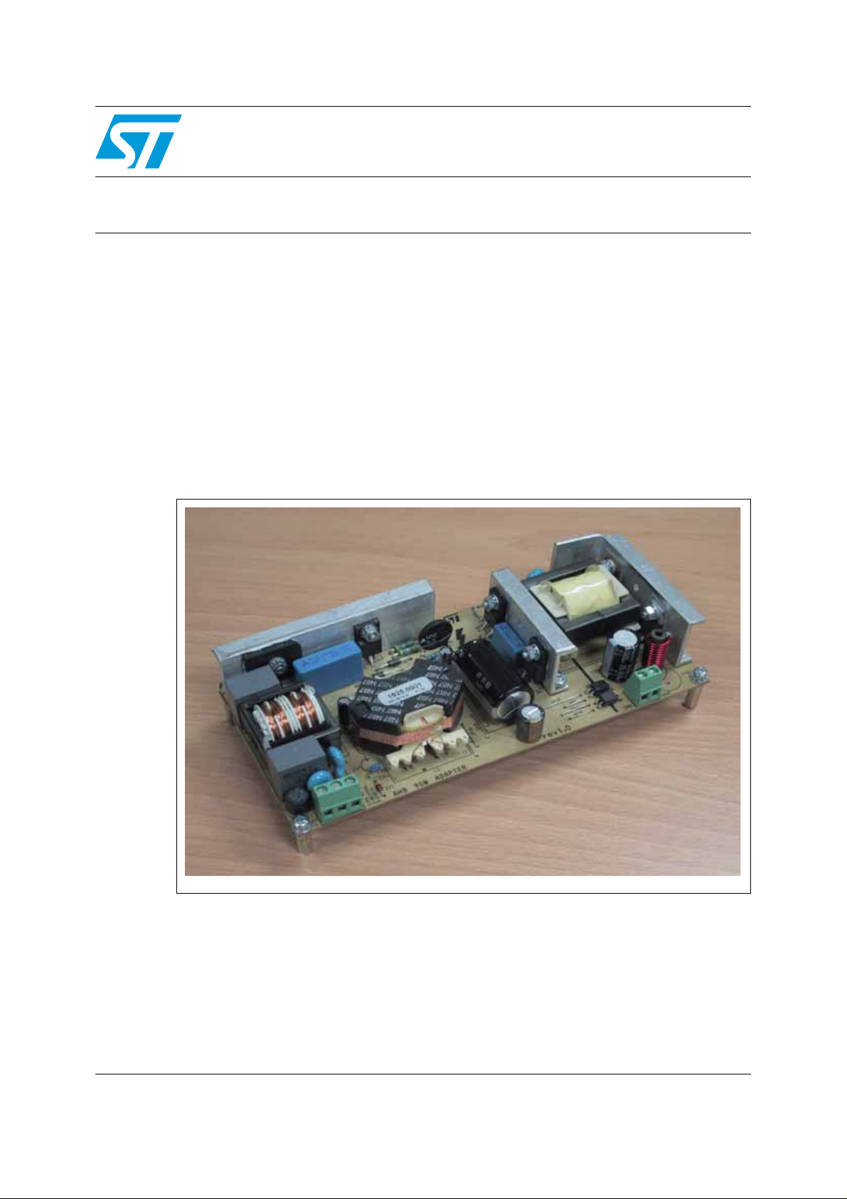
The order code for this de monstration board is EVL6591-90WADP.
Figure 1. EVL6591-90WADP demonstration board
AM01816v1
January 2009 Rev 1 1/35
www.st.com
Page 2

Contents AN2852
Contents
1 Main characteristics and circuit description . . . . . . . . . . . . . . . . . . . . . 4
2 Operating waveforms . . . . . . . . . . . . . . . . . . . . . . . . . . . . . . . . . . . . . . . . 7
2.1 Asymmetrical half-bridge (AHB) typical waveforms . . . . . . . . . . . . . . . . . . 7
2.2 Low-load operation . . . . . . . . . . . . . . . . . . . . . . . . . . . . . . . . . . . . . . . . . . 10
2.3 Short-circuit protection . . . . . . . . . . . . . . . . . . . . . . . . . . . . . . . . . . . . . . . 12
2.4 Overvoltage protection . . . . . . . . . . . . . . . . . . . . . . . . . . . . . . . . . . . . . . . 13
2.5 Startup sequence . . . . . . . . . . . . . . . . . . . . . . . . . . . . . . . . . . . . . . . . . . . 15
3 Electrical performance . . . . . . . . . . . . . . . . . . . . . . . . . . . . . . . . . . . . . . 17
3.1 Efficiency measurement and no-load consumption . . . . . . . . . . . . . . . . . 17
3.2 Harmonic content measurement . . . . . . . . . . . . . . . . . . . . . . . . . . . . . . . 20
4 Thermal measurements . . . . . . . . . . . . . . . . . . . . . . . . . . . . . . . . . . . . . 22
5 Conducted noise measurements (pre-compliance test) . . . . . . . . . . . 24
6 Bill of material . . . . . . . . . . . . . . . . . . . . . . . . . . . . . . . . . . . . . . . . . . . . . 25
7 PFC coil specifications . . . . . . . . . . . . . . . . . . . . . . . . . . . . . . . . . . . . . . 29
7.1 Electrical characteristics . . . . . . . . . . . . . . . . . . . . . . . . . . . . . . . . . . . . . . 29
7.2 Mechanical aspect and pin numbering . . . . . . . . . . . . . . . . . . . . . . . . . . . 30
8 AHB transformer specifications . . . . . . . . . . . . . . . . . . . . . . . . . . . . . . 31
8.1 Electrical characteristics . . . . . . . . . . . . . . . . . . . . . . . . . . . . . . . . . . . . . . 31
8.2 Mechanical aspect and pin numbering . . . . . . . . . . . . . . . . . . . . . . . . . . . 32
9 PCB layout . . . . . . . . . . . . . . . . . . . . . . . . . . . . . . . . . . . . . . . . . . . . . . . . 33
10 Revision history . . . . . . . . . . . . . . . . . . . . . . . . . . . . . . . . . . . . . . . . . . . 34
2/35
Page 3

AN2852 List of figures
List of figures
Figure 1. EVL6591-90WADP demonstration board. . . . . . . . . . . . . . . . . . . . . . . . . . . . . . . . . . . . . . . 1
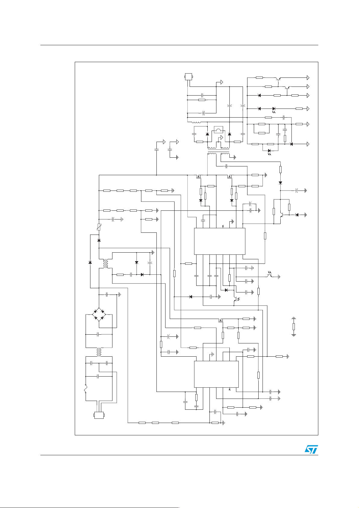
Figure 2. EVL6591-90WADP schematic . . . . . . . . . . . . . . . . . . . . . . . . . . . . . . . . . . . . . . . . . . . . . . . 6
Figure 3. AHB primary side key waveforms at full load . . . . . . . . . . . . . . . . . . . . . . . . . . . . . . . . . . . . 7
Figure 4. Detailed AHB zero-voltage switching at full load . . . . . . . . . . . . . . . . . . . . . . . . . . . . . . . . . 8
Figure 5. Detailed AHB zero-voltage switching at half load. . . . . . . . . . . . . . . . . . . . . . . . . . . . . . . . . 9
Figure 6. AHB secondary side key waveforms at full load. . . . . . . . . . . . . . . . . . . . . . . . . . . . . . . . . . 9
Figure 7. Burst mode at no load. . . . . . . . . . . . . . . . . . . . . . . . . . . . . . . . . . . . . . . . . . . . . . . . . . . . . 10
Figure 8. Detailed burst mode at no load. . . . . . . . . . . . . . . . . . . . . . . . . . . . . . . . . . . . . . . . . . . . . . 11
Figure 9. Load transitions . . . . . . . . . . . . . . . . . . . . . . . . . . . . . . . . . . . . . . . . . . . . . . . . . . . . . . . . . 11
Figure 10. Detailed short-circuit behavior . . . . . . . . . . . . . . . . . . . . . . . . . . . . . . . . . . . . . . . . . . . . . . 12
Figure 11. HICCUP mode . . . . . . . . . . . . . . . . . . . . . . . . . . . . . . . . . . . . . . . . . . . . . . . . . . . . . . . . . . 13
Figure 12. Detailed OVP intervention . . . . . . . . . . . . . . . . . . . . . . . . . . . . . . . . . . . . . . . . . . . . . . . . . 14
Figure 13. OVP intervention: system is latched. . . . . . . . . . . . . . . . . . . . . . . . . . . . . . . . . . . . . . . . . . 14
Figure 14. Complete startup sequence at 115Vac and full load . . . . . . . . . . . . . . . . . . . . . . . . . . . . . 15
Figure 15. Detailed startup sequence at 115Vac and full load . . . . . . . . . . . . . . . . . . . . . . . . . . . . . . 16
Figure 16. Efficiency vs. O/P power. . . . . . . . . . . . . . . . . . . . . . . . . . . . . . . . . . . . . . . . . . . . . . . . . . . 18
Figure 17. No-load consumption . . . . . . . . . . . . . . . . . . . . . . . . . . . . . . . . . . . . . . . . . . . . . . . . . . . . . 19
Figure 18. EN61000-3-2 measurements at full load . . . . . . . . . . . . . . . . . . . . . . . . . . . . . . . . . . . . . . 20
Figure 19. JEIDA-MITI measurements at full load. . . . . . . . . . . . . . . . . . . . . . . . . . . . . . . . . . . . . . . . 20
Figure 20. EN61000-3-2 measurements at 75 W input . . . . . . . . . . . . . . . . . . . . . . . . . . . . . . . . . . . . 20
Figure 21. JEIDA-MITI measurements at 75 W input . . . . . . . . . . . . . . . . . . . . . . . . . . . . . . . . . . . . . 20
Figure 22. PF vs. input voltage . . . . . . . . . . . . . . . . . . . . . . . . . . . . . . . . . . . . . . . . . . . . . . . . . . . . . . 21
Figure 23. THD vs. input voltage . . . . . . . . . . . . . . . . . . . . . . . . . . . . . . . . . . . . . . . . . . . . . . . . . . . . . 21
Figure 24. Thermal map at 115Vac - full load . . . . . . . . . . . . . . . . . . . . . . . . . . . . . . . . . . . . . . . . . . . 22
Figure 25. Thermal map at 230Vac - full load . . . . . . . . . . . . . . . . . . . . . . . . . . . . . . . . . . . . . . . . . . . 22
Figure 26. CE peak measure at 115Vac and full load . . . . . . . . . . . . . . . . . . . . . . . . . . . . . . . . . . . . . 24
Figure 27. CE peak measure at 230Vac and full load . . . . . . . . . . . . . . . . . . . . . . . . . . . . . . . . . . . . . 24
Figure 28. Electrical diagram . . . . . . . . . . . . . . . . . . . . . . . . . . . . . . . . . . . . . . . . . . . . . . . . . . . . . . . . 29
Figure 29. Bottom view . . . . . . . . . . . . . . . . . . . . . . . . . . . . . . . . . . . . . . . . . . . . . . . . . . . . . . . . . . . . 30
Figure 30. Electrical diagram . . . . . . . . . . . . . . . . . . . . . . . . . . . . . . . . . . . . . . . . . . . . . . . . . . . . . . . . 31
Figure 31. Windings position . . . . . . . . . . . . . . . . . . . . . . . . . . . . . . . . . . . . . . . . . . . . . . . . . . . . . . . . 32
Figure 32. Top view . . . . . . . . . . . . . . . . . . . . . . . . . . . . . . . . . . . . . . . . . . . . . . . . . . . . . . . . . . . . . . . 32
Figure 33. Topside silk screen. . . . . . . . . . . . . . . . . . . . . . . . . . . . . . . . . . . . . . . . . . . . . . . . . . . . . . . 33
Figure 34. Bottomside silk screen . . . . . . . . . . . . . . . . . . . . . . . . . . . . . . . . . . . . . . . . . . . . . . . . . . . . 33
Figure 35. Copper traces (bottomside) . . . . . . . . . . . . . . . . . . . . . . . . . . . . . . . . . . . . . . . . . . . . . . . . 33
3/35
Page 4

Main characteristics and circuit description AN2852
1 Main characteristics and circuit description
The main characteristics of the SMPS adapter are as follows:
● Input mains range
–Vin: 88 ~ 264 Vrms
– f: 45 ~ 66 Hz
● Output: 12Vdc ± 2% - 7.5 A
● No-load: Pin below 0.35 W
● Protections
– Short-circuit
–Overload
– Ouput overvoltage
– Brownout
● PCB type and size
–CEM-1
– Single-side 70 µm
– 174 x 78 mm
● Safety: according to EN60065
● EMI: according to EN50022 - class B
The adapter implements a two-stage solution. The front-end PFC uses a boost topology
working in transition mode (TM). The IC used is the L6563, advanced TM PFC controller,
which integrates all the functions an d protection needed to control the stage and an
interface with the downstream DC-DC converter.
The power stage of the PFC comprises inductor L2, MOSFET Q1, diode D4 and capacitor
C9. The PFC circuit is quite standard and already well described in previous ST application
notes. Therefore this note will f ocus on the AHB stage and its controller, the L6591. This DCDC converter comprises a half-bridge (MOSFET Q3 and Q4) connected to the output
voltage of the PFC stage that driv es the se ries connection of a DC blocking capacitor (C44)
and the primary of the transformer (T1). The tran sf ormer has two secondary windings with a
center tap connection tied to ground. The other ends are connected to the output diodes
D12 and D13. The output inductor is betw ee n th e co mmo n cathod e of diod es D1 2 and D1 3
and the output. The L6591 includes a current mode PWM control ler (fixed-frequency
solution), gate drivers for both low and high-side MOSFETs with integrated bootstrap diode
and all the functions and protections tailored for this topology. The device is housed in an
SO-16 narrow package.
This adapter uses the magnetizing current and the output inductor current ripple to obtain
the correct primary current direction to achieve zero-voltage switching (ZVS) at turn-on of
both MOSFETs. The transformer construction is quite simple as it is a layer type with the
primary winding split in two parts (sandwich configuration) and two secondary windings.
The primary leakage inductance is about 3% of the magnetizing inductance. The h alf-bridge
is operated at fixed frequency with complementary duty cycles on the two MOSFETs. The
high-side FET is on during the D time and the low-side FET is on for the 1-D time. C44 is
calculated in order to have a resonance frequency due to Lm and C44 well below the
switching frequency (t hat, in this applicat ion, has bee n set at abou t 100 kHz). In this way the
voltage on C44 is nearly constant and equal to Vin x D where Vin is the high-voltage input
4/35
Page 5

AN2852 Main characteristics and circuit description
bus and D is the duty cycle. For stability reasons related to the topology, the IC limits the
maximum duty cycle at 50%. The current in the primary tank circuit is read by the controller
thanks to the sense resistors R81 and R82. The self supply is basically obtained thanks to
an auxiliary winding on the AHB transformer. A small charge pump on the auxiliary windings
of the PFC inductor helps during the startup phase. A pin dedicated to startup sequencing, a
spare latched protection (dedicated here to out put overvoltage protecti on), the soft-start
function, the overload protection, an interface with the PFC controller and the integrated
high-voltage startup generator complete the features of the L6591. All the functions and
protections are detailed in the following sections.
5/35
Page 6
Main characteristics and circuit description AN2852
Figure 2. EVL6591-90WADP schematic
R30
J2
1
2
Output connector
12V-7.5A
C56
100NF
R97
N.M.
C46
25V
1000uF
+
L3
3.3uH
D12
STPS16L40CT
C58
1N8
9
R94
C21
C20
2N2
2N2
12R
T1
AHB Trafo
2
+
+
C62
N.M.
N.M.
C61
JP9
N.M.
10
12
4
5
C59
470PF
D13
STPS30100ST
14
R95
47R
6
R29
100K
BZV55-B11
D28
BZV55-B13
U5A
PC817
12
D25
R87
N.M.
R86
33K
C53
N.M.
R85
220K
R88
2K2
R83
6K8
12
U3A
2K2
BC847C
2 3
1 Q11
Q10
BC847C
2 3
R24
1.8K
1
R25
4.7K
R96
470
C55
N.M.
R93
3K3
C54
1uF
1
R91
U4
75K
TS3431
3 2
PC817
D3
1N4005
D1
F1
T4A
J1
R11
R7
2R5
R6
D4
STTH2L 06
L2
GBU6J
-+
C4
470NF
L1
86A-5163
4 8
1 5
C2
2N2
C1
470nF
1
2
3
Input connector
STP12NM50FP
C44
220NF
250V
Q3
R53
3M0
680K
+
C9
47uF
10 3
8 5
700uH
C5
470NF
400V
C3
2N2
88 - 264Vac
0R0
R12
3M0
680K
R8
450V
R70
33R
R13
8.2K
R28
24K9
10R
R72
D23
100NF
C14
LL4148
16
HVSTAR T
U2
L6591
LINE1DIS2ISEN3SS4OSC
R71
10R
C41
4N7
D27
LL4148
R19
56K
R100
0R0
14
VCC
INV
U1
1
R18
56K
C13
1uF
C42
100NF
15
BOOT
13
GD
COMP
2
R10
15K
R3
680K
R9
82K
C17
N.M.
D21
+
1N4148
D22
C40
10NF
LL4148
R98
220K
+
C15
22uF
0R0
R54
100NF
C39
R1
1M0
R2
R55
1M2
0R0
Q4
R73
100K
STP12N M50FP
R74
R75
14
HVG
C45 220PF
12
GND
MULT3CS4VFF5TBO6PFC_OK
10R
56R
D24
LL4148
11
12
13
N.C.
GND
FGND
VREF
6
5
C43 10NF
R78 19K6
LL4148
D29
2.2NF
U5B
C47
PC817
STP12NM50FP
Q1
R46
100K
R21
27R
10
11
9
ZCD
RUN
PWM_STOP
R15
C11
10NF
R14
18K
4
3
150K
10
LVG
COMP7PFC_STOP
8
PWM_LATCH
7
R82
0R82
R81
0R82
R79
100K
R77
56R
C51
22uF
+
C50
100NF
9
Vcc
8
C52
100NF
C48
6.8NF
C49
330PF
R23
0R47
R22
0R47
R20
0R0
C16
1N0
R80
1K0
R27
470
L6563
R26
240K
C12
470NF
R17
0R0
D26
R90
0R0
R84
220R
U3B
PC817
43
R99
15K
C10
1N0
C22
220PF
C57
STPS1L60A
R89
100uF
+
R69
N.M.
1
2 3
D20
N.M.
NM
Q9
R101
0R0
100K
AM01817v1
6/35
Page 7
AN2852 Operating waveforms
2 Operating waveforms
2.1 Asymmetrical half-bridge (AHB) typical waveforms
As mentioned before, this application note f ocuses on the AHB stage . This DC-DC conv erter
has the 400 V PFC bus as input and delivers 12 V at the output.
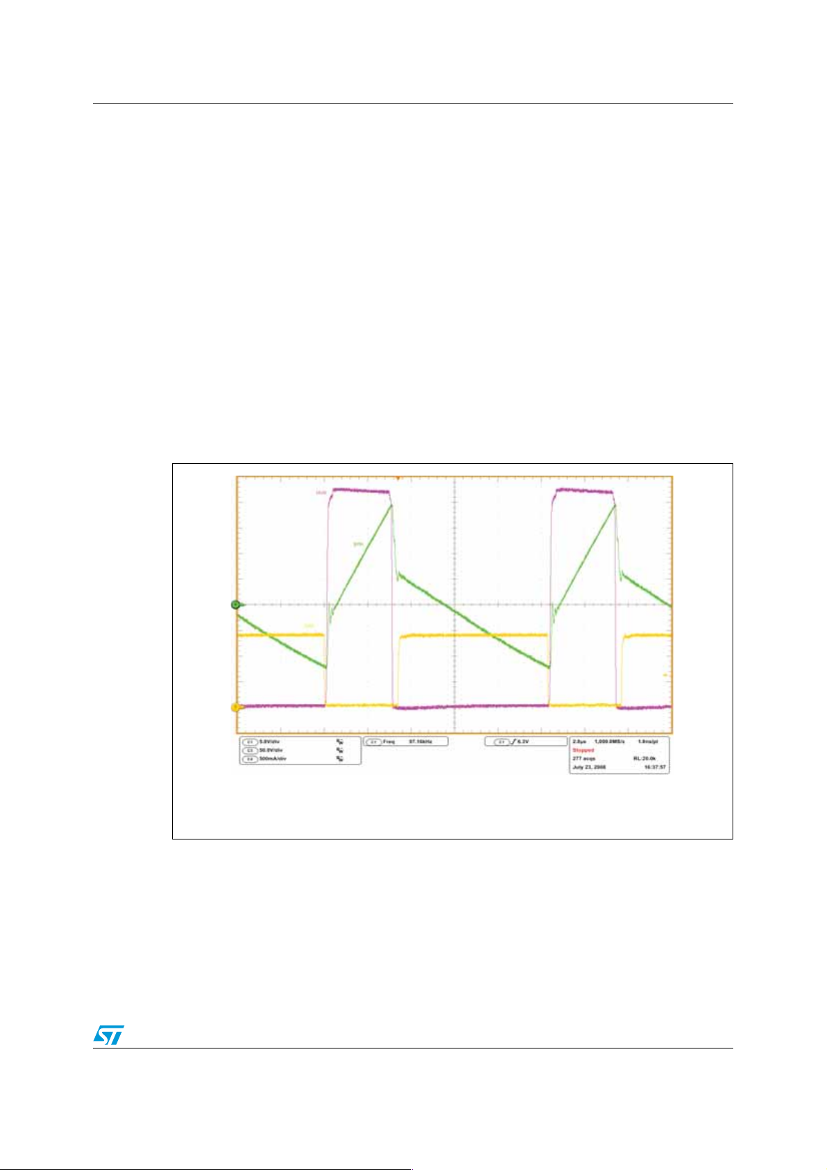
In Figure 3 the primary side key waveforms with full load applied are shown. Figure 4 shows
the detail of the two transition s during one s witching cycle. Wh en the LVG signal goes do wn,
the current is negative and so the half- bridge node (that has a certain capacitance value due
to the Coss of the MOSFETs and the stra y ca pacitance of the circuit) is cha rged up to 400 V.
After the deadtime has elapsed the high-side driver is turned on with zero volts across the
high-side MOSFET drain-source pins. The driver activation is visible on the HVG signal
when there is the small voltage step on the high part of the waveform.
When the high-side driver is turned off, the primary current is positive, so the half-bridge
node is discharged down to zero volts and the body diode of Q4 is activated. After the
deadtime the LVG turns on in ZVS condition.
Figure 3. AHB primary side key waveforms at full load
Ch1: LVG pin voltage (yellow)
Ch3: HVG pin voltage (purple)
Ch4: primary winding current (green)
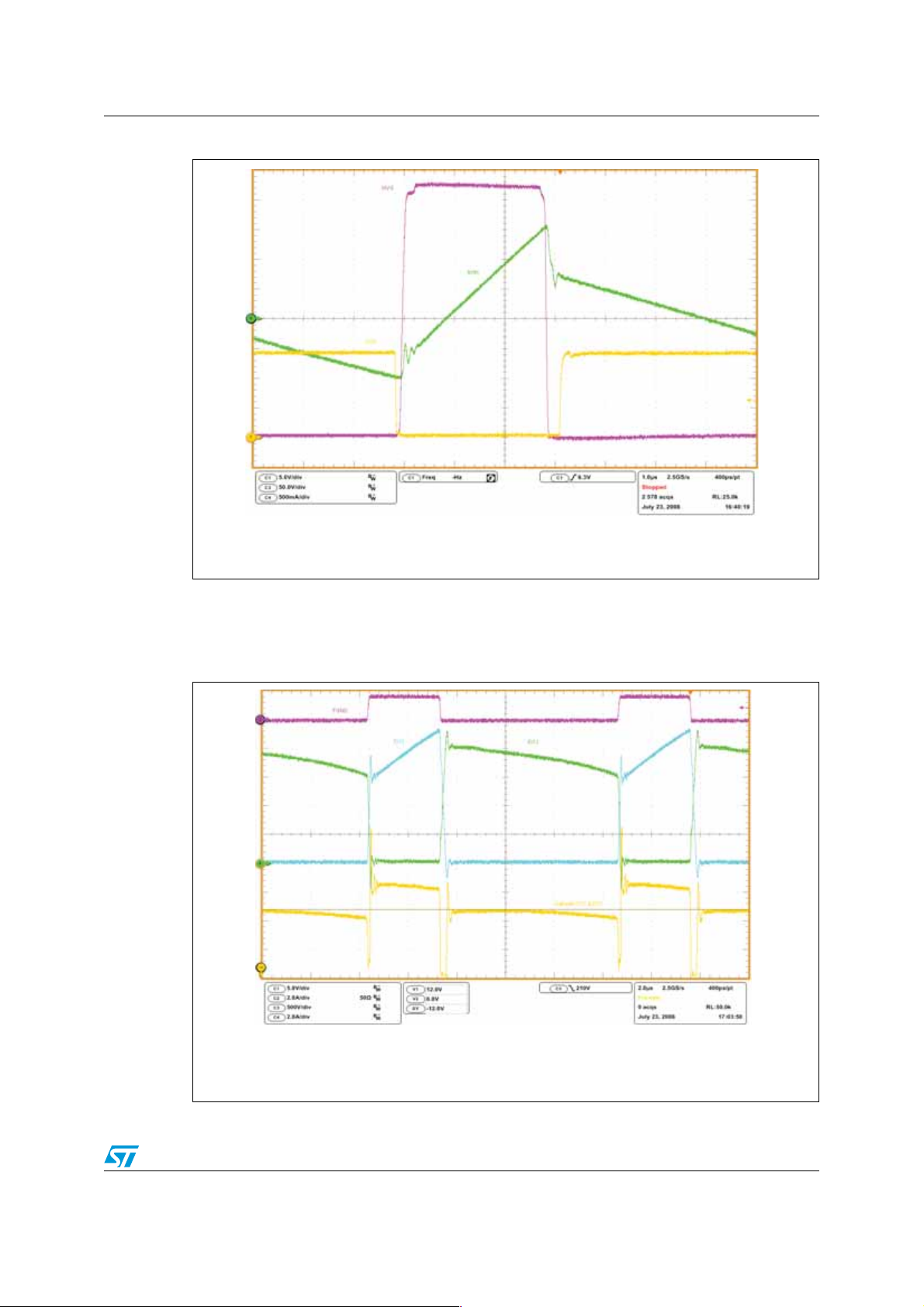
Typically, in the AHB topology, the most critical transition is the one between LVG turn-off
and HVG turn-on. In f act it is visibl e that the current a v ailable to mov e the half-bridge point is
less with respect to the other transition. This is due to the magnetizing current that is not
symmetrical with an average value of zero amps but has a certain offset due to the
asymmetrical driving of the tank circuit.
The fast current variation during transitions is due to the reversal of the current direction in
the secondary windings. The effort in this design was to maintain a negative current after
AM01818v1
7/35
Page 8
Operating waveforms AN2852
the positive variation at LVG turn-off. This was done by a correct design of the magnetizing
current, output inductor current ripple and choice of turns ratio.
Figure 4. Detailed AHB zero-voltage switching at full load
Ch1: LVG pin voltage (yellow)
Ch3: HVG pin voltage (purple)
Ch4: primary winding current (green)
AM01819v1
The ZVS condition is harder to meet as the load increases , so full load is the w orst condition
to have for a correct ZVS operation. In Figure 5 the same waveforms are shown with half
load. Since the output current is reduced, the fast primary side current variations are also
reduced and so the magnetizing current (that remains basically the same if the load
changes) becomes proportionally higher. The result is that there is more current available
for moving the half-bridge node.
8/35
Page 9
AN2852 Operating waveforms
Figure 5. Detailed AHB zero-voltage switching at half load
Ch1: LVG pin voltage (yellow)
Ch3: HVG pin voltage (purple)
Ch4: primary winding current (green)
AM01820v1
The key w av ef orms at the secondary side are shown in Figure 6. It is interesting to note that,
while the current is swapped between the two diodes, the voltage at their cathode is nearly
zero.
Figure 6. AHB secondary side key waveforms at full load
Ch1: D12 and D13 common cathode voltage (yellow)
Ch2: diode D12 current (blue)
Ch3: FGND pin voltage (purple)
Ch4: diode D13 current (green)
AM01821v1
9/35
Page 10
Operating waveforms AN2852
Another peculiarity of this topology is that, since it is asymmetrical, the diode D13 has to
carry higher average and RMS current and sustain higher reverse voltage with respect to
diode D12. This implies that D13 dissipates a lot mor e t han D12 an d ma kes sense, in order
to improve efficiency and save money, to have a synchronous rectification only on D13.
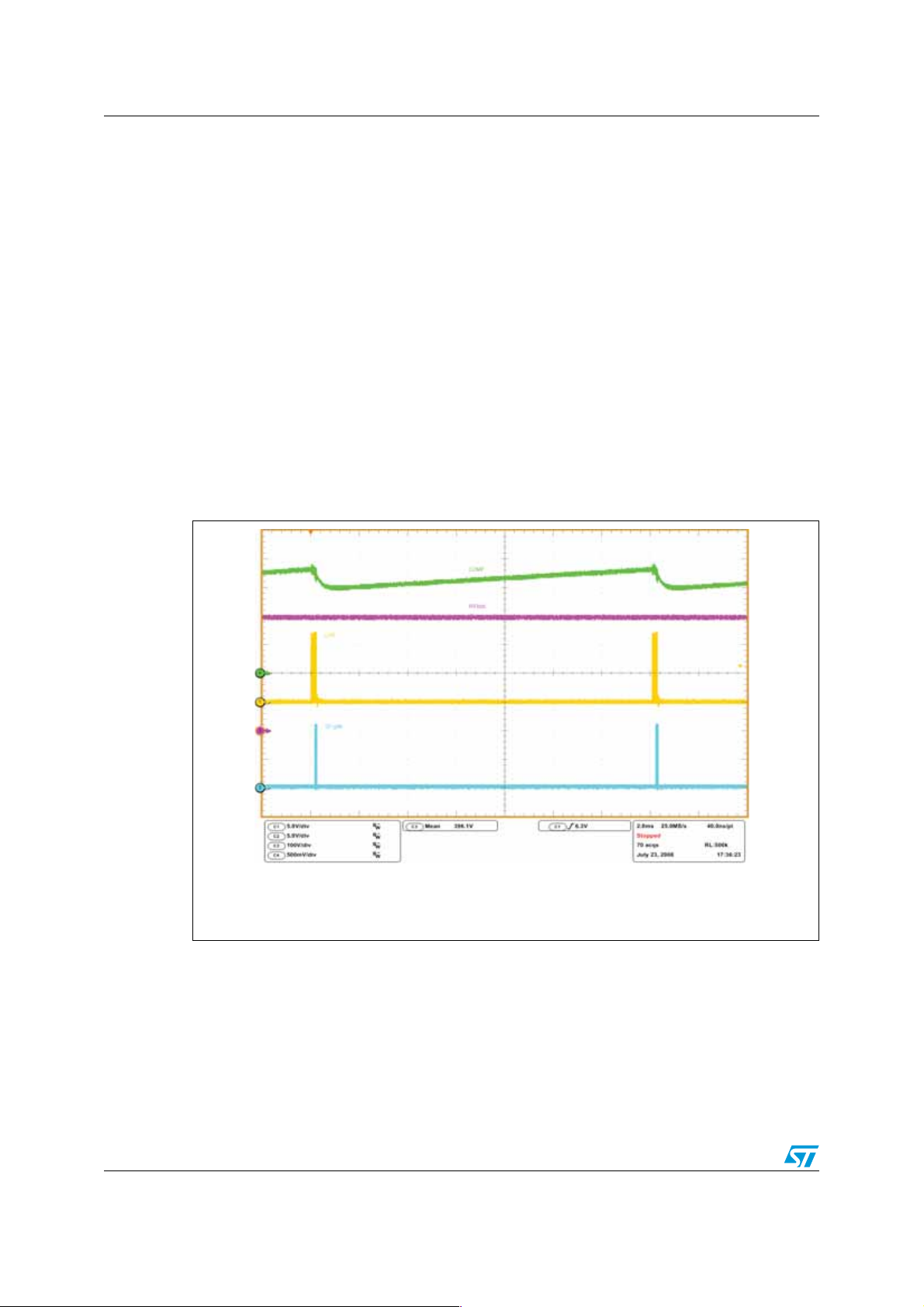
2.2 Low-load operation
At light loads (and no-load) conditions the system enters a controlled burst mode operation,
allowing input power reduction. The burst mode is activated according to the COMP pin
level.
In Figure 7 and Figure 8 the burst mode operation with no load is shown. Under a certain
load also the PFC stage works in burst mode operat ion (sp ecifically t he PFC enters in b ur st
mode for a load value higher than the one for the AHB). Using the PFC_STOP pin of the
L6591 and the PFC_OK pin of the L6563, a simple interface is built in order to keep the
burst modes of the two ICs synchronized. This operation allows fast response to a heavy
load transition since the PFC is already on when the power is needed. This avoids output
voltage dips. The load transition from 0 to 100% and vice versa can be seen in Figure 9.
Figure 7. Burst mode at no load
Ch1: LVG pin voltage (yellow)
Ch2: Q1 (PFC MOSFET) gate (blue)
Ch3:PFC output voltage
Ch4: COMP pin voltage (green)
10/35
AM01822v1
Page 11
AN2852 Operating waveforms
Figure 8. Detailed burst mode at no load
Ch1: LVG pin voltage (yellow)
Ch2: Q1 (PFC MOSFET) gate (blue)
Ch3:PFC output voltage
Ch4: L6563 PFC_OK pin voltage (green)
AM01823v1
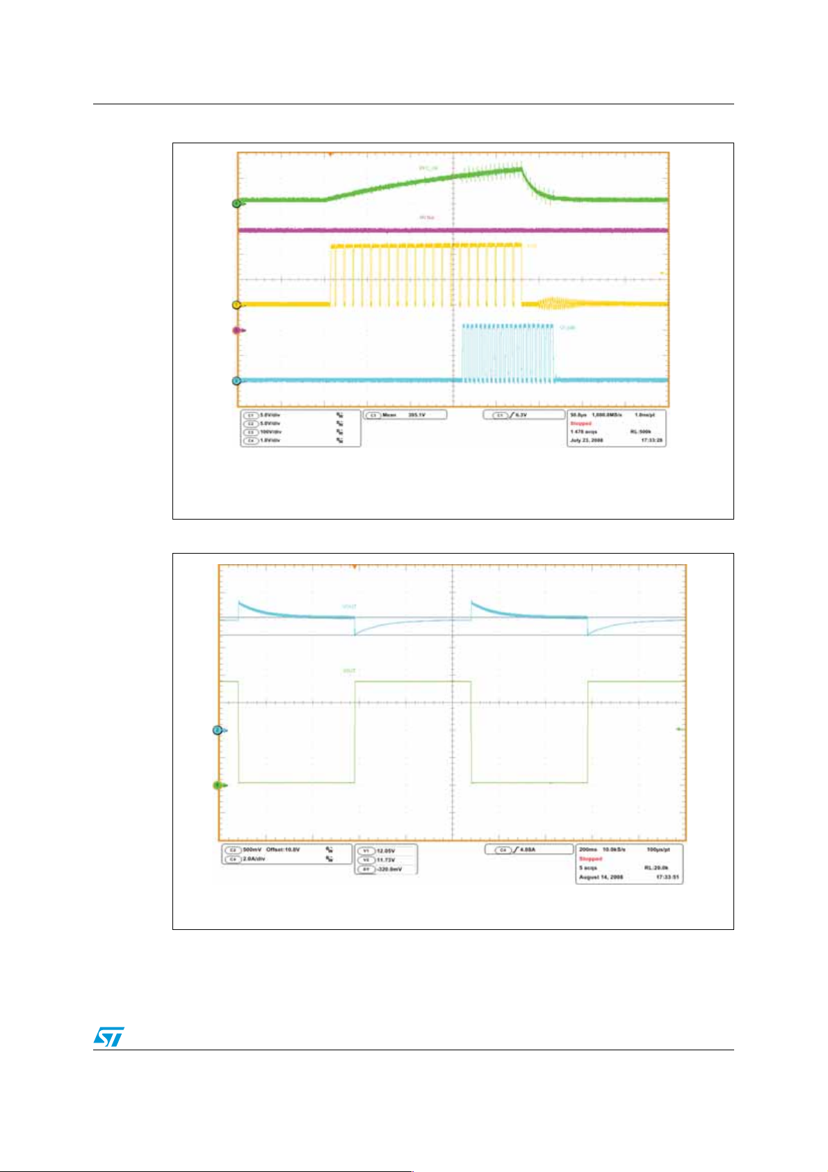
Figure 9. Load transitions
Ch2: output voltage (blue)
Ch4: output current (green)
AM01824v1
11/35
Page 12

Operating waveforms AN2852
2.3 Short-circuit protection
A short-circuit at the output activates the overload protection (OLP). Figure 10 shows the
pins involved in this function. When the short-circuit is applied, the COMP pin saturates
high. The IC detects this condition and starts charging the SS capacitor. When the SS
voltage reaches 5 V, the system shuts down. Diode D29 allows the SS voltage to be
clamped at about 5.4 V and the protection has an auto-restart behavior. If the short circuit is
not removed, the IC enters the HICCUP mode (Figure 11). When the IC is stopped by the
OLP, the high-voltage startup generator is invoked only when Vcc falls to 5 V (V
CCrestart
Thanks to this approach, the period between tw o restart trials is quite long which reduces
the stress on power components.
Figure 10. Detailed short-circuit behavior
).
Ch1: SS pin voltage (yellow)
Ch2: COMP pin voltage (blue)
Ch3: FGND pin voltage (purple)
Ch4: PFC_STOP pin voltage (green)
12/35
AM01825v1
Page 13

AN2852 Operating waveforms
Figure 11. HICCUP mode
Ch1: SS pin voltage (yellow)
Ch2: COMP pin voltage (blue)
Ch3: FGND pin voltage (purple)
Ch4: PFC_STOP pin voltage (green)
AM01826v1
2.4 Overvoltage protection
Since it is impossible to sense the output v oltage fr om the primary side in all load conditions,
the OVP senses such voltage directly on the output. A Zener diode (D25 ) is used as the
threshold to activate the protection. The information is passed to the controller using
optocoupler U5 that increases the di sable pin voltage over the intervention threshold of
4.5 V. In Figure 12 a loop failure is simulated by shorting R93. The overvoltage protection is
invoked and the output voltage reache s a maximum voltage of 14.8 V.
Since this protection uses the disab le pin, it is la tched. Hence, after PWM is stop ped, the HV
generator is invoked to keep Vcc voltage between 14 V and 13.5 V. Diode D27 brings the
PFC_OK pin voltage over 2.5 V, so the L6563 is also shut down and its consumption goes
almost to the startup level. The PWM_LATCH goes high which also keeps the disable pin
high. The latched operation is shown in Figure 13.
13/35
Page 14

Operating waveforms AN2852
Figure 12. Detailed OVP intervention
Ch1: output voltage (yellow)
Ch2: Vcc pin voltage (blue)
Ch3: FGND pin voltage (purple)
Ch4: DISABLE pin voltage (green)
AM01827v1
Figure 13. OVP intervention: system is latched
Ch2: Vcc pin voltage (blue)
Ch4: DISABLE pin voltage (green)
AM01828v1
14/35
Page 15

AN2852 Operating waveforms
2.5 Startup sequence
In this converter the startup sequence is quite particular and merits a detailed explanation.
When the mains is plugged in, the rectified input voltage is present on bulk capacitor C9.
Since this value is greater than 80 V , the HV sta rtup generator of the L6591 is turned on and
Vcc capacitors are charged with a constant current of about 0.75 mA. This charge time is
therefore independent of input voltage level. The L6563 has a turn-on threshold lower than
that of L6591, so the PFC controller starts first. The HV startup current is insufficient to
power the L6563, so a small charge pump (R70, C40, D21 and D22) is connected to the
PFC inductor auxiliary winding. With this circuit, when the L6563 starts, both Vcc voltage
and PFC output voltage increase.
Once Vcc > 14 V and line pin voltage is greater than 1.25 V , the L6591 also turns on. At this
point the charge pump is insufficient to sustain Vcc current of both ICs and so an auxiliary
winding on the AHB transformer is used to provide, together with the charge pump, the
power requested by the devices. The complete sequence is shown in Figure 14, while the
details of the turn-on of both ICs ar e sh own in Figure 15. Both figures show the startup at
115V ac mains inpu t. The startup at 230Vac is very similar, the only difference is that the Vcc
voltage during steady state operation is a little higher since the charge pump delivers more
current.
Figure 14. Complete startup sequen ce at 115Vac and full load
Ch1: LVG voltage (yellow)
Ch2: Vcc pin voltage (blue)
Ch3: PFC output voltage (purple)
Ch4: output voltage (green)
AM01829v1
15/35
Page 16

Operating waveforms AN2852
Figure 15. Detailed startup sequence at 115Vac and full load
Ch1: LVG voltage (yellow)
Ch2: Vcc pin voltage (blue)
Ch3: PFC output voltage (purple)
Ch4: output voltage (green)
AM01830v1
16/35
Page 17

AN2852 Electrical performance
3 Electrical performance
3.1 Efficiency measurement and no-load consumption
Table 1 and 2 give the efficiency measurements taken at the two nominal voltages.
Table 1. Efficiency at 115Vrms
Load [%] Iout [A] Vout [V] Pout [W] Pin [W] Eff [%]
5% 0.3746 12.12 4.54 6.80 66.77%
10% 0.7507 12.11 9.09 12.10 75.13%
20% 1.5037 12.10 18.19 21.9882.78%
25% 1.8787 12.09 22.71 26.83 84.66%
40% 3.0037 12.09 36.31 41.49 87.53%
50% 3.7537 12.08 45.34 51.41 88.20%
60% 4.5037 12.08 54.40 61.44 88.55%
75% 5.6287 12.07 67.94 76.67 88.61%
80% 6.0037 12.07 72.46 81.77 88.62%
100% 7.5037 12.06 90.49 102.4888.30%
Table 2. Efficiency at 230Vrms
Load [%] Iout [A] Vout [V] Pout [W] Pin [W] Eff [%]
5% 0.3746 12.12 4.54 6.58 68.97%
10% 0.7507 12.11 9.09 12.41 73.26%
20% 1.5037 12.10 18.19 22.30 81.59%
25% 1.8787 12.09 22.71 27.02 84.06%
40% 3.0037 12.08 36.28 41.37 87.71%
50% 3.7537 12.08 45.34 51.05 88.82%
60% 4.5037 12.07 54.36 60.83 89.36%
75% 5.6287 12.07 67.94 75.60 89.87%
80% 6.0037 12.07 72.46 80.56 89.95%
100% 7.5037 12.06 90.49 100.55 90.00%
17/35
Page 18

Electrical performance AN2852
The efficiency taken at 25%, 50%, 75% and 100% of rated load allows calculating the
average efficiency required by the ENERGY STAR
®
specification.
Table 3. Average efficiency for EPA
Vin [Vrms] Average efficiency for EPA
115 87.44%
230 88.19%
Table 4 shows the no-load consumption. The adapter has good values (about 300 mW at
230Vac), considering that it is a two-stage system with the PFC stage always on.
Table 4. No-load consumption
Vin [Vac] 90 115 135 180 230 264
Pin [W] 0.215 0.225 0.235 0.255 0.290 0.315
This adapter meets the two conditions required by ENERGY STAR
®
specification version
2.0 (average efficiency > 87% and no-load input power < 0.5 W) for an external power
supply (EPS). Therefore this SMPS is EPA 2.0 compliant.
Figure 16 shows the graph of the efficiency vs. output power while Figure 17 shows the
graph of the input power vs. input voltage with no load applied.
Figure 16. Efficiency vs. O/P power
92.00%
90.00%
88.00%
86.00%
84.00%
82.00%
80.00%
78.00%
76.00%
74.00%
72.00%
70.00%
68.00%
66.00%
020406080100
Efficiency
115Vac
230Vac
Output power [W]
AM01831v1
18/35
Page 19

AN2852 Electrical performance
Input voltage [Vac]
Input power [W]
Figure 17. No-load consumption
0.350
0.300
0.250
0.200
0.150
0.100
0.050
0.000
50 100 150 200 250 300
AM01832v1
Some measurements with low output loads were also taken, refer to Table 5 and Table 6.
Table 5. Low-load efficiency at 115Vrms
Pout [W] Iout [mA] Vout [V] Pin [W] Eff [%]
1.50 124.50 12.12 2.696 55.97%
1.00 82.50 12.12 1.883 53.10%
0.50 42.02 12.12 1.076 47.31%
0.25 21.05 12.11 0.654 38.98%
Table 6. Low-load efficiency at 230Vrms
Pout [W] Iout [mA] Vout [V] Pin [W] Eff [%]
1.50 124.50 12.12 2.598 58.08%
1.00 82.50 12.12 1.802 55.49%
0.50 42.02 12.12 1.08746.83%
0.25 21.05 12.11 0.704 36.21%
19/35
Page 20

Electrical performance AN2852
Harmonic order (n)
Harmonic current (A)
Measurements @ 230Vac Full load EN61000-3-2 class D limits
0.0001
0.001
0.01
0.1
1
1 3 5791113 15 17 19 21 23 25 27 29 31 33 35 37 39
Harmonic order (n)
Harmonic current (A)
Measurements @ 230Vac 75W in EN61000-3-2 class D limits
0.0001
0.001
0.01
0.1
1
1 3 5791113 15 17 19 21 23 25 27 29 31 33 35 37 39
Harmonic order (n)
Harmonic current (A)
Measurements @ 100Vac 75W in JEIDA-MITI class D limits
3.2 Harmonic content measurement
The front-end PFC stage provides the reduction of the mains harmonic, allowing meeting
European EN61000-3-2 and Japanese JEIDA-MITI standards for class D equipment.
Figure 18 and 19 show the harmonic contents of the mains current at full load.
A measure has been done also with 75 W input power which is the lower limit for using
harmonic reduction techniques.
Figure 18. EN61000-3-2 measurements at full
0.0001
load
1
0.1
0.01
0.001
1 3 5791113 15 17 19 21 23 25 27 29 31 33 35 37 39
AM01833v1
Figure 20. EN61000-3-2 measur ements at 75 W
input
Figure 19. JEIDA-MITI measurements at full
load
10
Measurements @ 100Vac Full load JEIDA-MITI class D limits
1
0.1
0.01
Harmonic current (A)
0.001
0.0001
1 3 5791113 15 17 19 21 23 25 27 29 31 33 35 37 39
Harmonic order (n)
AM01834v1
Figure 21. JEIDA-MITI measurements at 75 W
input
20/35
AM01835v1
AM01836v1
Page 21

AN2852 Electrical performance
0.850
0.875
0.900
0.925
0.950
0.975
1.000
80 120 160 200 240 280
Vin [Vrms]
PF
Full load 75 W in
0.00
1.00
2.00
3.00
4.00
5.00
6.00
7.00
8.00
9.00
Vin [Vrms]
THD [%]
Full load 75 W in
To evaluate the performance of the PFC stage also, the PF and THD vs. input voltage
graphs are shown in Figure 22 and 23 at full load and 75 W input power.
Figure 22. PF vs. input voltage
AM01837v1
Figure 23. THD vs. input voltage
80 120 160 200 240 280
AM01838v1
21/35
Page 22

Thermal measurements AN2852
4 Thermal measurements
A thermal analysis of the board was performed using an IR camera, refer to Figure 24 and
25.
Figure 24. Thermal map at 115Vac - full load
Figure 25. Thermal map at 230Vac - full load
°C
°C
90.0
81.9
73.8
65.6
57.5
49.4
41.3
33.1
25.0
90.0
81.9
73.8
65.6
57.5
49.4
AM01839v1
Table 7. T emperature of key components (T
points)
Point Reference T [°C] at 115Vac T [°C] at 230Vac
A D1 (Input bridge) 49.5 39.5
B Q1 (PFC MOSFET) 46.4 37.9
C D4 (PFC diode) 56.8 49.1
D R6 (NTC) 55.9 47.1
E L2 (PFC coil) 38.1 35.7
F Q4 (AHB low-side MOSFET) 43.8 39.2
22/35
41.3
33.1
25.0
= 25 °C, emissivity = 0.95 for all
amb
AM01840v1
Page 23

AN2852 Thermal measurements
Table 7. T emperature of key components (T
= 25 °C, emissivity = 0.95 for all
amb
points) (continued)
Point Reference T [°C] at 115Vac T [°C] at 230Vac
G Q3 (AHB high side MOSFET) 40.2 39.3
H T1 (AHB transformer ferrite) 64.8 63.4
I T1 (AHB transformer winding) 81.2 80.1
J D13 (AHB output diode) 83.1 81.8
K D12 (AHB output diode) 73.7 72.8
L L3 (Output inductor) 58.7 57.9
23/35
Page 24

Conducted noise measurements (pre-compliance test) AN2852
5 Conducted noise measurements (pre-compliance
test)
Figure 26 and 27 show the conducted noise measurements performed at the two nominal
voltages with peak detect ion and considering only the w or st phase. Both measures are well
below the average limit (taken from EN55022 CLASS B norm).
Figure 26. CE peak measure at 115Vac and full load
Figure 27. CE peak measure at 230Vac and full load
AM01841v1
AM01842v1
24/35
Page 25

AN2852 Bill of material
6 Bill of material
Table 8. EVL6591-90WADP bill of materials
Ref Value Description Manufacturer
C1 470 NF Polypropylene X2 capacitor - R46 KI 3470--02 M Arcotronics
C10 1N0 SMD ceramic capacitor X7R - 50 V AVX
C11 10 NF SMD ceramic capacitor X7R - 50 V AVX
C12 470 NF SMD ceramic capacitor X7R - 25 V AVX
C13 1 µF SMD ceramic capacitor X7R - 25 V AVX
C14 100 NF SMD ceramic capacitor X7R - 50 V AVX
C15 22 µF Electrolytic capacitor YXF - 50 V Rubycon
C16 1N0 SMD ceramic capacitor X7R - 50 V AVX
C17 N.M. Electrolytic capacitor
C2 2N2 Ceramic Y1 capacitor - DE1E3KX222M Murata
C20 2N2 Ceramic Y1 capacitor - DE1E3KX222M Murata
C21 2N2 Ceramic Y1 capacitor - DE1E3KX222M Murata
C22 220 PF SMD ceramic capacitor NP0 - 50 V AVX
C3 2N2 Ceramic Y1 capacitor - DE1E3KX222M Murata
C39 100 NF SMD ceramic capacitor X7R - 50 V AVX
C4 470 NF Polypropylene X2 capacitor - R46 KI 3470--02 M Arcotronics
C40 10 NF Ceramic capacitor X7R - 50 V AVX
C41 4N7 SMD ceramic capacitor X7R - 50 V AVX
C42 100 NF SMD ceramic capacitor X7R - 50 V AVX
C43 10 NF SMD ceramic capacitor X7R - 50 V AVX
C44 220 NF Polypropylene capacitor - B32652A3224J EPCOS
C45 220 PF SMD ceramic capacitor NP0 - 50 V AVX
C46 1000 µF Electrolytic capacitor ZL - 25 V Rubycon
C47 2.2 NF SMD ceramic capacitor X7R - 50 V AVX
C48 6.8 NF SMD ceramic capacitor X7R - 50 V AVX
C49 330 PF SMD ceramic capacitor NP0 - 50 V - 2% AVX
C5 470 NF Polypropylene capacitor - PHE426KD6470JR06L2 EVOX-RIFA
C50 100 NF SMD ceramic capacitor X7R - 50 V AVX
C51 22 uF Electrolytic capacitor YXF - 50 V Rubycon
C52 100 NF SMD ceramic capacitor X7R - 50 V AVX
C53 N.M. SMD ceramic capacitor X7R - 50 V
C54 1 uF SMD ceramic capacitor X7R - 25 V AVX
25/35
Page 26

Bill of material AN2852
Table 8. EVL6591-90WADP bill of materials (continued)
Ref Value Description Manufacturer
C55 N.M. SMD ceramic capacitor X7R - 50 V
C56 100 NF SMD ceramic capacitor X7R - 50 V AVX
C57 100 µF Electrolytic capacitor YXF - 35 V Rubycon
C58 1N8 SMD ceramic capacitor X7R - 50 V AVX
C59 470 PF SMD ceramic capacitor X7R - 50 V AVX
C61 N.M. Electrolytic capacitor
C62 N.M. Electrolytic capacitor
C9 47 µF Electrolytic capacitor - 450 V - EEUED2W470 Panasonic
D1 GBU6J Bridge rectifier Vishay
D12 STPS16L40CT Power Schottky rectifier STMicroelectronics
D13 STPS30100ST Power Schottky rectifier STMicroelectronics
D20 N.M. Zener diode
D21 1N4148 Diode
D22 LL4148 SMD diode
D23 LL4148 SMD diode
D24 LL4148 SMD diode
D25 BZV55-B13 Zener diode - 2% Vishay
D26 STPS1L60A SMD Schottky diode STMicroelectronics
D27 LL4148 SMD diode
D28 BZV55-B11 Zener diode - 2% Vishay
D29 LL4148 SMD diode
D3 1N4005 Diode Vishay
D4 STTH2L06 Ultrafast diode STMicroelectronics
F1 T4 A PCB fuse TR5 Wickmann
J1 IN connector Screw connector - MKDS 1,5/3-5.08 Phoenix Contact
J2 OUT connector Screw connector - MKDS 1,5/2-5.08 Phoenix Contact
JP9 N.M. Wire jumper
L1 2x25 mH Input EMI filter - HF2826-253Y1R2-T01 TDK
L2 700 µH PFC inductor - 1825.0001 Magnetica
L3 3.3 µH Power inductor - PCV-0-332-10L Coilcraft
Q1 STP12NM50FP Power MOSFET STMicroelectronics
Q10 BC847C Small signal BJT
Q11 BC847C Small signal BJT
Q3 STP12NM50FP Power MOSFET STMicroelectronics
Q4 STP12NM50FP Power MOSFET STMicroelectronics
26/35
Page 27

AN2852 Bill of material
Table 8. EVL6591-90WADP bill of materials (continued)
Ref Value Description Manufacturer
Q9 N.M. Small signal BJT
R1 1M0 SMD film resistor - 5% - 250 ppm/°C - 1206 Vishay
R10 15 kΩ SMD film resistor - 1% - 100 ppm/°C - 0805 Vishay
R100 0R0 SMD film resistor - 1206 Vishay
R101 0R0 SMD film resistor - 1206 Vishay
R11 3M0 Film resistor - 1% - 100 ppm/°C - 0.4W Vishay
R12 3M0 Film resistor - 1% - 100 ppm/°C - 0.4W Vishay
R13 8.2 kΩ SMD film resistor - 1% - 100 ppm/°C - 0805 Vishay
R14 18 kΩ SMD film resistor - 5% - 250 ppm/°C - 1206 Vishay
R15 150 kΩ SMD film resistor - 5% - 250 ppm/°C - 1206 Vishay
R17 0R0 SMD film resistor - 1206 Vishay
R18 56 kΩ SMD film resistor - 5% - 250 ppm/°C - 0805 Vishay
R19 56 kΩ SMD film resistor - 5% - 250 ppm/°C - 0805 Vishay
R2 1M2 SMD film resistor - 5% - 250 ppm/°C - 1206 Vishay
R20 0R0 SMD film resistor - 1206 Vishay
R21 27 Ω SMD film resistor - 5% - 250 ppm/°C - 1206 Vishay
R22 0R47 Film resistor – 5% – 250 ppm/°C - 0.4W Vishay
R23 0R47 Film resistor – 5% – 250 ppm/°C - 0.4W Vishay
R24 1.8 kΩ SMD film resistor - 1% - 100 ppm/°C - 0805 Vishay
R25 4.7 kΩ SMD film resistor - 1% - 100 ppm/°C - 0805 Vishay
R26 240 kΩ SMD film resistor - 5% - 250 ppm/°C - 0805 Vishay
R27 470 SMD film resistor - 5% - 250 ppm/°C - 1206 Vishay
R28 24K9 SMD film resistor - 1% - 100 ppm/°C - 0805 Vishay
R29 100 kΩ SMD film resistor - 5% - 250 ppm/°C - 0805 Vishay
R3 680 kΩ Film resistor - 1% - 100 ppm/°C - 1206 Vishay
R30 2K2 SMD film resistor - 1% - 100 ppm/°C - 1206 Vishay
R46 100 kΩ SMD film resistor - 5% - 250 ppm/°C - 0805 Vishay
R53 0R0 SMD film resistor - 1206 Vishay
R54 0R0 SMD film resistor - 1206 Vishay
R55 0R0 SMD film resistor - 1206 Vishay
R6 2R5 NTC resistor S237 - B57237S0259M000 EPCOS
R69 N.M. SMD resistor - 0805 Vishay
R7 680 kΩ Film resistor - 1% - 100 ppm/°C - 0.4 W Vishay
R70 33 Ω SMD film resistor - 5% - 250 ppm/°C - 1206 Vishay
R71 10
Ω SMD film resistor - 5% - 250 ppm/°C - 1206 Vishay
27/35
Page 28

Bill of material AN2852
Table 8. EVL6591-90WADP bill of materials (continued)
Ref Value Description Manufacturer
R72 10 Ω SMD film resistor - 5% - 250 ppm/°C - 0805 Vishay
R73 100 kΩ SMD film resistor - 5% - 250 ppm/°C - 0805 Vishay
R74 10 Ω SMD film resistor - 5% - 250 ppm/°C - 0805 Vishay
R75 56 Ω SMD film resistor - 5% - 250 ppm/°C - 0805 Vishay
R77 56 Ω SMD film resistor - 5% - 250 ppm/°C - 0805 Vishay
R78 19K6 SMD film resistor - 1% - 100 ppm/°C - 0805 Vishay
R79 100 kΩ SMD film resistor - 5% - 250 ppm/°C - 0805 Vishay
R8 680 kΩ Film resistor - 1% - 100 ppm/°C - 0.4 W Vishay
R80 1K0 SMD film resistor - 5% - 250 ppm/°C - 0805 Vishay
R810R82 SMD film resistor - 5% - 250 ppm/°C - 1206 Vishay
R820R82 SMD film resistor - 5% - 250 ppm/°C - 1206 Vishay
R836K8 SMD film resistor - 5% - 250 ppm/°C - 0805 Vishay
R84 220 Ω SMD film resistor - 5% - 250 ppm/°C - 1206 Vishay
R85220 kΩ SMD fi lm resistor - 1% - 100 ppm/°C - 0805 Vishay
R86 33 kΩ SMD film resistor - 1% - 100 ppm/°C - 0805 Vishay
R87 N.M. SMD resistor - 0805 Vishay
R88 2K2 SMD film resistor - 5% - 250 ppm/°C - 0805 Vishay
R89100 kΩ SMD fi lm resistor - 5% - 250 ppm/°C - 1206 Vishay
R9 82 k
R90 0R0 SMD film resistor – 0805 Vishay
R91 75 kΩ SMD film resistor - 5% - 250 ppm/°C - 0805 Vishay
R93 3K3 SMD film resistor - 1% - 100 ppm/°C - 0805 Vishay
R94 12 Ω SMD film resistor - 5% - 250 ppm/°C - 1206 Vishay
R95 47 Ω SMD film resistor - 5% - 250 ppm/°C - 1206 Vishay
R96 470 SMD film resistor - 1% - 100 ppm/°C - 1206 Vishay
R97 N.M. SMD resistor - 1206 Vishay
R98 220 Ω SMD film resistor - 5% - 250 ppm/°C - 1206 Vishay
R99 15 kΩ SMD film resistor - 5% - 250 ppm/°C - 1206 Vishay
T1 Transformer AHB transformer 1754.0004 Magnetica
U1 L6563 Advanced TM PFC controller STMicroelectronics
U2 L6591 PWM controller for ZVS half-bridge STMicroelectronics
U3 PC817 Optocoupler - PC817X1J000F Sharp
U4 TS3431AILT SMD voltage reference - 1% STMicroelectronics
Ω SMD film resistor - 1% - 100 ppm/°C - 0805 Vishay
U5 PC817 Optocoupler - PC817X1J000F Sharp
28/35
Page 29

AN2852 PFC coil specifications
8
10
7 PFC coil specifications
● Application type: consumer, IT
● Transformer type: open
● Coil former: vertical type, 6+6 pins
● Max. temp. rise: 45°C
● Max. operating ambient temp.: 60°C
● Mains insulation: N.A.
7.1 Electrical characteristics
● Converter topology: boost, transition mode
● Core type: RM14 - N87 or equivalent
● Min. operating frequency: 20 kHz
● Primary inductance: 700 µH 10% at 1 kHz - 0.25 V (see Note 1)
● Peak primary current: 3.5 A
●
RMS primary curre n t: 1. 25 A
Note: 1 measured between pins 3-5
pk
RMS
.
Figure 28. Electrical diagram
3
AUXPRIM
5
Table 9. Winding characteristics
Pins Winding RMS current Nr. of turns Wire type
3 – 5 Primary 1.25 A
8 – 10 AUX
1. Auxiliary winding is wound on top of primary winding
(1)
0.05 A
RMS
RMS
53 Stranded 7 x Ø 0.28 mm – G2
4 spaced Ø 0.28 mm – G2
AM01843v1
29/35
Page 30

PFC coil specifications AN2852
7.2 Mechanical aspect and pin numbering
● Maximum height from PCB: 22 mm
● Coil former type: vertical, 6+6 pins
● Pin distance: 5.08 mm
● Row distance: 35.56 mm
● Pins removed: # 1, 4, 6, 7, 9, 11, 12
● External copper shield: bare, wound around the ferrite core including the windings a nd
coil former. Height is 7 mm. Connected by a solid wire soldered to pin 10
● Manufacturer: Magnetica
● P/N: 1825.0001.
Figure 29. Bottom view
6
1
7
12
AM01844v1
30/35
Page 31

AN2852 AHB transformer specifications
8 AHB transformer specifications
● Application type: consumer, IT
● Transformer type: open
● Coil former: horizontal type, 7+7 pins
● Max. temp. rise: 45°C
● Max. operating ambient temp.: 60°C
● Mains insulation: compliance with EN60950.
8.1 Electrical characteristics
● Converter topology: asymmetrical half-bridge
● Core type: ETD34 - N87 or equivalent
● Operating frequency: 100 kHz
● Primary inductance: 400 µH 10% at 1 kHz - 0.25 V (see Note 1)
● Air gap: 2.32 mm on central leg
● Leakage inductance: 10 µH max. at 100 kHz - 0.25 V (see Note 2)
● Primary capacitance: 6 pF typ. (see Note 3)
● Max. peak primary current: 1.93 A
●
RMS primary curre n t: 0. 75 A
Note: 1 measured between pins 2-4
2 measured between pins 2-4 with secondaries and auxiliary windings shorted
3 calculated considering primary inductance and resonance frequency
pk
RMS
Figure 30. Electrical diagram
PRIM.
AUX
2
4
5
6
9
10
12
14
SEC.
SEC.
AM01845v1
31/35
Page 32

AHB transformer specifications AN2852
Table 10. Winding characteristics
Pins Winding RMS current Nr. of turns Wire type
2 – 3 Primary A 0.75 A
9 – 10 Secondary 1 3.81 A
12 – 14 Secondary 2 6.57 A
3 – 4 Primary B 0.75 A
5 – 6 Auxiliary 0.0 5 A
Note: Primaries A and B are in series
Cover wires ends with silicon sleeve
Figure 31. Windings position
3mm
COIL FORMER
RMS
RMS
RMS
RMS
RMS
AUX
PRIMARY - B
SECONDARY 2
SECONDARY 1
PRIMARY - A
35 Ø 0.355 mm – G2
4 Stranded 90 x Ø 0.1 mm – G1
7 Stranded 135 x Ø 0.1 mm – G1
35 Ø 0.355 mm – G2
3 spaced Ø 0.355 mm – G2
3mm
INSULATING
TAPE
AM01846v1
8.2 Mechanical aspect and pin numbering
● Maximum height from PCB: 30 mm
● Coil former type: vertical, low profile, 7+7 pins, NORWE ETD34lr/h14/-1/rtg
● Pin distance: 5.08 mm
● Row distance: 25.4 mm
● Pin removed: # 7
● Manufacturer: Magnetica
● P/N: 1754.0004
Figure 32. Top view
1
7
14
8
AM01847v1
32/35
Page 33

AN2852 PCB layout
9 PCB layout
Figure 33. Topside silk screen
AM01848v1
Figure 34. Bottomside silk screen
Figure 35. Copper traces (bottomside)
AM01849v1
AM01850v1
33/35
Page 34

Revision history AN2852
10 Revision history
Table 11. Document revision history
Date Revision Changes
28-Jan-2009 1 Initial release
34/35
Page 35

AN2852
Please Read Carefully:
Information in this document is provided solely in connection with ST products. STMicroelectronics NV and its subsidiaries (“ST”) reserve the
right to make changes, corrections, modifications or improvements, to this document, and the products and services described herein at any
time, without notice.
All ST products are sold pursuant to ST’s terms and conditions of sal e.
Purchasers are solely res ponsibl e fo r the c hoic e, se lecti on an d use o f the S T prod ucts and s ervi ces d escr ibed he rein , and ST as sumes no
liability whatsoever relati ng to the choice, selection or use of the ST products and services de scribed herein.
No license, express or implied, by estoppel or otherwise, to any intellectual property rights is granted under this document. If any part of this
document refers to any third pa rty p ro duc ts or se rv ices it sh all n ot be deem ed a lice ns e gr ant by ST fo r t he use of su ch thi r d party products
or services, or any intellectua l property c ontained the rein or consi dered as a warr anty coverin g the use in any manner whats oever of suc h
third party products or servi ces or any intellectual property contained therein.
UNLESS OTHERWISE SET FORTH IN ST’S TERMS AND CONDITIONS OF SALE ST DISCLAIMS ANY EXPRESS OR IMPLIED
WARRANTY WITH RESPECT TO THE USE AND/OR SALE OF ST PRODUCTS INCLUDING WITHOUT LIMITATION IMPLIED
WARRANTIES OF MERCHANTABILITY, FITNESS FOR A PARTICUL AR PURPOS E (AND THEIR EQUIVALE NTS UNDER THE LAWS
OF ANY JURISDICTION), OR INFRINGEMENT OF ANY PATENT, COPYRIGHT OR OTHER INTELLECTUAL PROPERTY RIGHT.
UNLESS EXPRESSLY APPROVED IN WRITING BY AN AUTHORIZED ST REPRESENTATIVE, ST PRODUCTS ARE NOT
RECOMMENDED, AUTHORIZED OR WARRANTED FOR USE IN MILITARY, AIR CRAFT, SPACE, LIFE SAVING, OR LIFE SUSTAINING
APPLICATIONS, NOR IN PRODUCTS OR SYSTEMS WHERE FAILURE OR MALFUNCTION MAY RESULT IN PERSONAL INJ URY,
DEATH, OR SEVERE PROPERTY OR ENVIRONMENTAL DAMAGE. ST PRODUCTS WHICH ARE NOT SPECIFIED AS "AUTOMOTIVE
GRADE" MAY ONLY BE USED IN AUTOMOTIVE APPLICATIONS AT USER’S OWN RISK.
Resale of ST products with provisions different from the statements and/or technical features set forth in this document shall immediately void
any warranty granted by ST fo r the ST pro duct or serv ice describe d herein and shall not cr eate or exten d in any manne r whatsoever , any
liability of ST.
ST and the ST logo are trademarks or registered trademarks of ST in various countries.
Information in this document su persedes and replaces all info rmation previously supplied .
The ST logo is a registered trademark of STMicroelectronics. All other names are the property of their respective owners.
© 2009 STMicroelectronics - All rights reserved
STMicroelectronics group of compan ie s
Australia - Belgium - Brazil - Canada - China - Czech Republic - Finland - France - Germany - Hong Kong - India - Israel - Italy - Japan -
Malaysia - Malta - Morocco - Singapore - Spain - Sweden - Switzerland - United Kingdom - United States of America
www.st.com
35/35
 Loading...