

Page 1

AN2847
Application note
LIS331DLH: ±2 g /±4 g /±8 g digital output
high performance ultra low-power 3-axis accelerometer
Introduction
This document provides application information for the low-voltage 3-axis digital output
linear MEMS accelerometer provided in the LGA package.
The LIS331DLH is a high performance ultra low-power 3-axis linear accelerometer, which
belongs to the “nano” family of MEMS accelerometers, with digital I
standard output.
The device features ultra low-power operational modes that allow advanced power saving
and smart Sleep to Wakeup functions.
The LIS331DLH has dynamically user-selectable full scales of ±2 g /±4 g /±8 g and is
capable of measuring acceleration with output data rates from 0.5 Hz to 1 kHz.
The self-test capability allows the user to check the functioning of the sensor in the final
application.
The device can be configured to generate interrupt signals in response to inertial wakeup/free-fall events, or based on the position of the device itself.
The thresholds and timing of interrupt generators are programmable by the end user while
fully operational. The LIS331DLH is available in a small, thin plastic land grid array (LGA)
package, and is guaranteed to operate over a wide temperature range of -40 °C to +85 °C.
2
C/SPI serial interface
September 2010 Doc ID 15136 Rev 2 1/31
www.st.com
Page 2

Contents AN2847
Contents
1 Register table . . . . . . . . . . . . . . . . . . . . . . . . . . . . . . . . . . . . . . . . . . . . . . . 6
2 Start-up sequence . . . . . . . . . . . . . . . . . . . . . . . . . . . . . . . . . . . . . . . . . . . 7
2.1 Reading acceleration data . . . . . . . . . . . . . . . . . . . . . . . . . . . . . . . . . . . . . 8
2.1.1 Using the status register . . . . . . . . . . . . . . . . . . . . . . . . . . . . . . . . . . . . . 8
2.1.2 Using the data-ready signal . . . . . . . . . . . . . . . . . . . . . . . . . . . . . . . . . . . 8
2.1.3 Using the block data update feature . . . . . . . . . . . . . . . . . . . . . . . . . . . . 8
2.2 Output data rate selection and reading timing . . . . . . . . . . . . . . . . . . . . . . 9
2.3 Data ready vs. interrupt signal . . . . . . . . . . . . . . . . . . . . . . . . . . . . . . . . . 10
2.4 Understanding acceleration data . . . . . . . . . . . . . . . . . . . . . . . . . . . . . . . 11
2.4.1 Data alignment . . . . . . . . . . . . . . . . . . . . . . . . . . . . . . . . . . . . . . . . . . . . 11
2.4.2 Big-little endian selection . . . . . . . . . . . . . . . . . . . . . . . . . . . . . . . . . . . . 11
2.4.3 Example of acceleration data . . . . . . . . . . . . . . . . . . . . . . . . . . . . . . . . 11
3 Operating modes . . . . . . . . . . . . . . . . . . . . . . . . . . . . . . . . . . . . . . . . . . . 13
3.1 Normal mode . . . . . . . . . . . . . . . . . . . . . . . . . . . . . . . . . . . . . . . . . . . . . . 14
3.2 Power down mode . . . . . . . . . . . . . . . . . . . . . . . . . . . . . . . . . . . . . . . . . . 14
3.3 Low power mode . . . . . . . . . . . . . . . . . . . . . . . . . . . . . . . . . . . . . . . . . . . 15
3.4 Sleep to wake . . . . . . . . . . . . . . . . . . . . . . . . . . . . . . . . . . . . . . . . . . . . . . 15
3.4.1 Entering the sleep to wake mode . . . . . . . . . . . . . . . . . . . . . . . . . . . . . 16
3.4.2 Exiting the sleep to wake mode . . . . . . . . . . . . . . . . . . . . . . . . . . . . . . . 16
4 High pass filter . . . . . . . . . . . . . . . . . . . . . . . . . . . . . . . . . . . . . . . . . . . . 17
4.1 Filter configuration . . . . . . . . . . . . . . . . . . . . . . . . . . . . . . . . . . . . . . . . . . 17
4.1.1 Normal mode . . . . . . . . . . . . . . . . . . . . . . . . . . . . . . . . . . . . . . . . . . . . . 18
4.1.2 Reference mode . . . . . . . . . . . . . . . . . . . . . . . . . . . . . . . . . . . . . . . . . . 18
5 Interrupt generation . . . . . . . . . . . . . . . . . . . . . . . . . . . . . . . . . . . . . . . . 20
5.1 Duration . . . . . . . . . . . . . . . . . . . . . . . . . . . . . . . . . . . . . . . . . . . . . . . . . . 20
5.2 Threshold . . . . . . . . . . . . . . . . . . . . . . . . . . . . . . . . . . . . . . . . . . . . . . . . . 21
5.3 Free-fall and wake-up interrupts . . . . . . . . . . . . . . . . . . . . . . . . . . . . . . . . 21
5.4 Inertial wake-up . . . . . . . . . . . . . . . . . . . . . . . . . . . . . . . . . . . . . . . . . . . . 24
5.4.1 HP filter bypassed . . . . . . . . . . . . . . . . . . . . . . . . . . . . . . . . . . . . . . . . . 24
2/31 Doc ID 15136 Rev 2
Page 3

AN2847 Contents
5.4.2 Using the HP filter . . . . . . . . . . . . . . . . . . . . . . . . . . . . . . . . . . . . . . . . . 25
5.5 Free-fall detection . . . . . . . . . . . . . . . . . . . . . . . . . . . . . . . . . . . . . . . . . . . 25
5.6 6D direction . . . . . . . . . . . . . . . . . . . . . . . . . . . . . . . . . . . . . . . . . . . . . . . 26
6 Revision history . . . . . . . . . . . . . . . . . . . . . . . . . . . . . . . . . . . . . . . . . . . 30
Doc ID 15136 Rev 2 3/31
Page 4

List of tables AN2847
List of tables
Table 1. Register table . . . . . . . . . . . . . . . . . . . . . . . . . . . . . . . . . . . . . . . . . . . . . . . . . . . . . . . . . . . . 6
Table 2. Output data rate . . . . . . . . . . . . . . . . . . . . . . . . . . . . . . . . . . . . . . . . . . . . . . . . . . . . . . . . . . 9
Table 3. Timing value to prevent data loss . . . . . . . . . . . . . . . . . . . . . . . . . . . . . . . . . . . . . . . . . . . . . 9
Table 4. Data signal on INT 1 and INT 2 pads . . . . . . . . . . . . . . . . . . . . . . . . . . . . . . . . . . . . . . . . . 10
Table 5. Output data register content vs. acceleration (FS = 2 g) . . . . . . . . . . . . . . . . . . . . . . . . . . 12
Table 6. Power mode and low-power output data rate configurations . . . . . . . . . . . . . . . . . . . . . . . 13
Table 7. CTRL_REG1 - data rate . . . . . . . . . . . . . . . . . . . . . . . . . . . . . . . . . . . . . . . . . . . . . . . . . . . 13
Table 8. CTRL_REG5 - sleep to wake configuration . . . . . . . . . . . . . . . . . . . . . . . . . . . . . . . . . . . . 14
Table 9. Power consumption - normal mode (µA) . . . . . . . . . . . . . . . . . . . . . . . . . . . . . . . . . . . . . . 14
Table 10. Power consumption - low power mode (µA) . . . . . . . . . . . . . . . . . . . . . . . . . . . . . . . . . . . . 14
Table 11. Turn on time . . . . . . . . . . . . . . . . . . . . . . . . . . . . . . . . . . . . . . . . . . . . . . . . . . . . . . . . . . . . 15
Table 12. High-pass filter mode configuration . . . . . . . . . . . . . . . . . . . . . . . . . . . . . . . . . . . . . . . . . . 17
Table 13. High-pass filter cut-off frequency configuration . . . . . . . . . . . . . . . . . . . . . . . . . . . . . . . . . 18
Table 14. Reference mode LSB value . . . . . . . . . . . . . . . . . . . . . . . . . . . . . . . . . . . . . . . . . . . . . . . . 18
Table 15. Interrupt mode configuration . . . . . . . . . . . . . . . . . . . . . . . . . . . . . . . . . . . . . . . . . . . . . . . . 20
Table 16. Duration LSB value in normal mode . . . . . . . . . . . . . . . . . . . . . . . . . . . . . . . . . . . . . . . . . . 20
Table 17. Duration LSB value in low power mode . . . . . . . . . . . . . . . . . . . . . . . . . . . . . . . . . . . . . . . 21
Table 18. Threshold LSB value . . . . . . . . . . . . . . . . . . . . . . . . . . . . . . . . . . . . . . . . . . . . . . . . . . . . . 21
Table 19. INTx_SRC register in 6D position . . . . . . . . . . . . . . . . . . . . . . . . . . . . . . . . . . . . . . . . . . . . 29
Table 20. Document revision history . . . . . . . . . . . . . . . . . . . . . . . . . . . . . . . . . . . . . . . . . . . . . . . . . 30
4/31 Doc ID 15136 Rev 2
Page 5

AN2847 List of figures
List of figures
Figure 1. Reading timing . . . . . . . . . . . . . . . . . . . . . . . . . . . . . . . . . . . . . . . . . . . . . . . . . . . . . . . . . . . 9
Figure 2. Interrupt and DataReady signal generation block diagram . . . . . . . . . . . . . . . . . . . . . . . . . 10
Figure 3. Data-ready signal . . . . . . . . . . . . . . . . . . . . . . . . . . . . . . . . . . . . . . . . . . . . . . . . . . . . . . . . 11
Figure 4. Sleep to wake mode . . . . . . . . . . . . . . . . . . . . . . . . . . . . . . . . . . . . . . . . . . . . . . . . . . . . . . 16
Figure 5. High pass filter connections block diagram . . . . . . . . . . . . . . . . . . . . . . . . . . . . . . . . . . . . 17
Figure 6. HP_FILTER_RESET readings . . . . . . . . . . . . . . . . . . . . . . . . . . . . . . . . . . . . . . . . . . . . . . 18
Figure 7. Reference mode . . . . . . . . . . . . . . . . . . . . . . . . . . . . . . . . . . . . . . . . . . . . . . . . . . . . . . . . . 19
Figure 8. Free-fall, wake-up interrupt generator . . . . . . . . . . . . . . . . . . . . . . . . . . . . . . . . . . . . . . . . 22
Figure 9. FF_WU_CFG high and low. . . . . . . . . . . . . . . . . . . . . . . . . . . . . . . . . . . . . . . . . . . . . . . . . 23
Figure 10. Inertial wake-up interrupt . . . . . . . . . . . . . . . . . . . . . . . . . . . . . . . . . . . . . . . . . . . . . . . . . . 24
Figure 11. Free-fall interrupt . . . . . . . . . . . . . . . . . . . . . . . . . . . . . . . . . . . . . . . . . . . . . . . . . . . . . . . . 26
Figure 12. ZH, ZL, YH, YL, XH, XL behavior . . . . . . . . . . . . . . . . . . . . . . . . . . . . . . . . . . . . . . . . . . . . 27
Figure 13. 6D movement vs. 6D position . . . . . . . . . . . . . . . . . . . . . . . . . . . . . . . . . . . . . . . . . . . . . . . 28
Figure 14. 6D recognized positions . . . . . . . . . . . . . . . . . . . . . . . . . . . . . . . . . . . . . . . . . . . . . . . . . . . 28
Doc ID 15136 Rev 2 5/31
Page 6

Register table AN2847
1 Register table
Table 1. Register table
Register name Address Bit7 Bit6 Bit5 Bit4 Bit3 Bit2 Bit1 Bit0
WHO_AM_I 0Fh 0 0 1 1 0 0 1 0
CTRL_REG1 20h PM2 PM1 PM0 DR1 DR0 Zen Yen Xen
CTRL_REG2 21h BOOT HPM1 HPM0 FDS HPen2 HPen1 HPCF1 HPCF0
CTRL_REG3 22h IHL PP_OD LIR2 I2_CF1 I2_CF0 LIR1 I1_CF1 I1_CF0
CTRL_REG4 23h BDU BLE FS1 FS0 STsign 0 ST SIM
CTRL_REG5 24h - - - - - - TurnOn1 TurnOn0
HP_FILTER_RESET 25h - - - - - - - -
REFERENCE 26h REF7 REF6 REF5 REF4 REF3 REF2 REF1 REF0
STATUS_REG 27h ZYXOR ZOR YOR XOR ZYXDA ZDA YDA XDA
OUTX_L 28h XD7 XD6 XD5 XD4 XD3 XD2 XD1 XD0
OUTX_H 29h XD15 XD14 XD13 XD12 XD11 XD10 XD9 XD8
OUTY_L 2Ah YD7 YD6 YD5 YD4 YD3 YD2 YD1 YD0
OUTY_H 2Bh YD15 YD14 YD13 YD12 YD11 YD10 YD9 YD8
OUTZ_L 2Ch ZD7 ZD6 ZD5 ZD4 ZD3 ZD2 ZD1 ZD0
OUTZ_H 2Dh ZD15 ZD14 ZD13 ZD12 ZD11 ZD10 ZD9 ZD8
INT1_CFG 30h AOI 6D ZHIE ZLIE YHIE YLIE XHIE XLIE
INT1_SRC 31h - IA ZH ZL YH YL XH XL
INT1_THS 32h 0 THS6 THS5 THS4 THS3 THS2 THS1 THS0
INT1_DURATION 33h 0 D6 D5 D4 D3 D2 D1 D0
INT2_CFG 34h AOI 6D ZHIE ZLIE YHIE YLIE XHIE XLIE
INT2_SRC 35h - IA ZH ZL YH YL XH XL
INT2_THS 36h 0 THS6 THS5 THS4 THS3 THS2 THS1 THS0
INT2_DURATION 37h 0 D6 D5 D4 D3 D2 D1 D0
6/31 Doc ID 15136 Rev 2
Page 7

AN2847 Start-up sequence
2 Start-up sequence
Once the device is powered up it automatically downloads the calibration coefficients from
the embedded Flash memory to the internal registers. When the boot procedure is complete
(i.e. after about 5 milliseconds), the device automatically enters power-down mode.
To turn on the device and gather acceleration data, it is necessary to select one of the
operating modes through the CTRL_REG1 register, and to enable at least one of the axes.
The following general-purpose sequence can be used to configure the device:
1. write CTRL_REG1
2. write CTRL_REG2
3. write CTRL_REG3
4. write CTRL_REG4
5. write Reference
6. write INT1_THS
7. write INT1_DUR
8. write INT2_THS
9. write INT2_DUR
10. read HP_FILTER_RESET (if filter is enabled)
11. write INT1_CFG
12. write INT2_CFG
13. write CTRL_REG5
Register values can be changed at any time, and with the device in any operating mode.
Modifications take effect immediately.
Note that in case of changes in full scale, ODR or enabling/disabling of self-test, the output
of the device will require 1 ms + 1/ODR to settle (see Table 11). If the HP filter cut-off
frequency is changed, the filter can be reset by reading the HP_FILTER_RESET register.
Doc ID 15136 Rev 2 7/31
Page 8

Start-up sequence AN2847
2.1 Reading acceleration data
2.1.1 Using the status register
The device features a STATUS_REG register which should be polled to check when a new
set of data is available. The reading procedure is the following:
1 read STATUS_REG
2 if STATUS_REG(3) = 0 then goto 1
3 if STATUS_REG(7) = 1 then some data have been overwritten
4 read OUTX_L
5 read OUTX_H
6 read OUTY_L
7 read OUTY_H
8 read OUTZ_L
9 read OUTZ_H
10 data processing
11 goto 1
The check performed at step 3 determines whether the reading rate is adequate compared
to the data production rate. In cases where one or more acceleration samples have been
overwritten by new data due to an excessively slow reading rate, the ZYXOR bit of the
STATUS_REG register is set to 1.
The overrun bits are automatically cleared when all the data present inside the device have
been read and new data have not been produced in the meantime.
2.1.2 Using the data-ready signal
The device may be configured to have one HW signal to determine when a new set of
measurement data is available for reading. This signal is represented by the XYZDA bit of
the STATUS_REG register. The signal can be driven to the INT1 or INT2 pins and its polarity
set to active-low or active-high through the CTRL_REG3 register. The interrupt is reset
when the higher part of the data of all the enabled channels has been read.
2.1.3 Using the block data update feature
If the reading of the acceleration data is particularly slow and cannot be (or does not need to
be) synchronized with either the XYZDA bit within the STATUS_REG or with the RDY signal,
it is strongly recommended to set the BDU (block data update) bit in CTRL_REG4 to 1.
This feature prevents the need to read the values (most significant and least significant parts
of the acceleration data) related to different samples. In particular, when the BDU is
activated, the data registers related to each channel always contain the most recent
acceleration data produced by the device. But if the reading of a given pair (i.e. OUTX_H
and OUTX_L, OUTY_H and OUTY_L, OUTZ_H and OUTZ_L) is initiated, the refresh for
that pair is blocked until both the MSB and LSB parts of the data are read.
8/31 Doc ID 15136 Rev 2
Page 9
AN2847 Start-up sequence
Note: BDU only guarantees that OUTX(Y, Z)_L and OUTX(X,Z)_H have been sampled at the
same moment. If the reading speed is too low, it is possible, for example, to read X and Y
sampled at T1 and Z sampled at T2.
2.2 Output data rate selection and reading timing
The output data rate is user selectable through the DRx bits of the CTRL_REG1 (20h)
register. At power-on-reset, the DRx are reset to 0, thus providing a default output data rate
of 50 Hz.
The analog signal coming from the mechanical sensor is filtered by a low pass filter before
being converted by the internal ADC. The frequency at -3 dB of the low pass filter
determines the effective system resolution. The cut-off frequency depends on the DR<1:0>
bits in the CTRL_REG1 (20h) register (Table 2).
Table 2. Output data rate
DR1, DR0 Output data rate
00 50 Hz 37 Hz
01 100 Hz 74 Hz
10 400 Hz 292 Hz
11 1000 Hz 780 Hz
Analog filter
cut-off frequency (-3 dB)
Note: The output data rate precision is related to the internal oscillator; an error of +/- 10% should
be taken into account.
A typical reading period is defined which is 616 µs shorter than the output data rate period,
in order to prevent the loss of any data produced. During this time period the reading of the
data must be performed and the DataReady signal can be used as a trigger to begin the
reading sequence. At the end of the complete sequence, the DataReady signal goes down
and the rising edge that follows signals that new data are available. If this minimum reading
frequency is not observed, some data loss is possible and the DataReady signal is no
longer considered a trigger signal. The status register can be used to infer the occurrence of
an overrun.
Figure 1. Reading timing
4
44
.EWDATAAVAILABLE
$ATA2EADY
Table 3. Timing value to prevent data loss
Time Description Typ
T0 Data rate 1/ODR
Doc ID 15136 Rev 2 9/31
".W
Page 10
Start-up sequence AN2847
Table 3. Timing value to prevent data loss
Time Description Typ
T1 Reading period T0-T2
T2 New data generation 616 µs
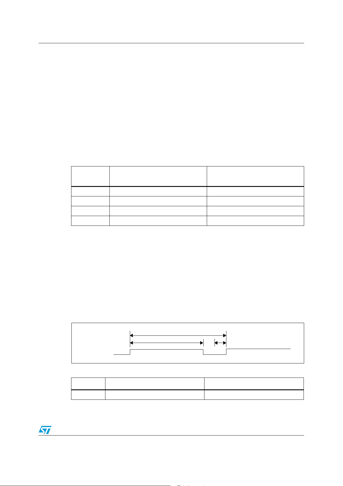
2.3 Data ready vs. interrupt signal
The device has two pins which can be activated to generate either the data-ready signal or
the interrupt signal. The functionality of the pins is selected acting on bit I1(2)_CFGx bits of
the CTRL_REG3 register, according to Table 4 and the block diagram shown in Figure 2.
Table 4. Data signal on INT 1 and INT 2 pads
I1(2)_CFG1 I1(2)_CFG0 INT 1(2) Pin
0 0 Interrupt 1 (2) source
0 1 Interrupt 1 source OR Interrupt 2 source
1 0 Data ready
1 1 Boot running
Figure 2. Interrupt and DataReady signal generation block diagram
/$2#LOCK
&REE&ALL
7AKE5P
)NTERRUPT
'ENERATOR
&REE&ALL
7AKE5P
)NTERRUPT
'ENERATOR
)!
).4?32#
/$2#LOCK
)!
).4?32#
#OUNTER
).4X?$52!4 )/.
#OUNTER
).4X?$52!4)/.
,ATCH
#42,?2%',)2
,ATCH
#42,?2%',)2
$ATA2EADY
3IGNAL
'ENERATOR
$ATA2EADYSIGNAL
"//4
TO
).4
0AD
)?#&'
)?#&'
".W
In particular, the data-ready (DR) signal rises to 1 when a new set of acceleration data has
been generated and is available for reading. The signal is reset after all the enabled
channels are read through the serial interface.
10/31 Doc ID 15136 Rev 2
Page 11

AN2847 Start-up sequence
Figure 3. Data-ready signal
.ELPMA3LECC!.ELPMA3LECC!!4!$,%##!
2$9
$!4!2%!$
89:89:
".W
2.4 Understanding acceleration data
The measured acceleration data are sent to the OUTX_H, OUTX_L, OUTY_H, OUTY_L,
OUTZ_H and OUTZ_L registers. These registers contain, respectively, the most significant
part and the least significant part of the acceleration signals acting on the X, Y and Z axes.
The complete acceleration data for the X (Y, Z) channel is given by the concatenation
OUTX_H & OUTX_L (OUTY_H & OUTY_L, OUTZ_H & OUTZ_L) and is expressed as a 2’s
complement number.
2.4.1 Data alignment
Acceleration data are represented as 16-bit numbers and are left justified.
2.4.2 Big-little endian selection
The LIS331DLH allows the swapping of the content of the lower and the upper part of the
acceleration registers (i.e. OUTX_H with OUTX_L), to be compliant with both little-endian
and big-endian data representations.
“Little endian” means that the low-order byte of the number is stored in memory at the
lowest address, and the high-order byte at the highest address (the little end comes first).
This mode corresponds to bit BLE in the CTRL_REG4 reset to 0 -default configuration-.
Conversely, “big endian” means that the high-order byte of the number is stored in memory
at the lowest address, and the low-order byte at the highest address.
2.4.3 Example of acceleration data
The following table provides a few basic examples of the data that will be read in the data
registers when the device is subject to a given acceleration. The values listed in the table
are based on the assumption that the device is perfectly calibrated (i.e., no offset, no gain
error, etc.) and show the effect of the BLE bit.
Doc ID 15136 Rev 2 11/31
Page 12

Start-up sequence AN2847
Table 5. Output data register content vs. acceleration (FS = 2 g)
BLE = 0 BLE = 1
Acceleration
values
28h 29h 28h 29h
0 g 00h 00h 00h 00h
350 mg E0h 15h 15h E0h
1 g 00h 40h 40h 00h
-350 mg 20h EAh EAh 20h
-1g 00h C0H C0H 00h
Register address
12/31 Doc ID 15136 Rev 2
Page 13

AN2847 Operating modes
3 Operating modes
The LIS331DLH can operate in the following four modes, which can be selected through the
configuration of CTR_REG1 and CTRL_REG5:
● Normal mode
● Power down
● Low power
● Sleep to wake
With reference to the datasheet of the device, the PowerMode (PM) and DataRate (DR) bits
of CTRL_REG1 register are used to select the basic operating modes (Power Down, Normal
mode and Low Power). The TurnOn bits of the CTRL_REG5 register are used to enable
Sleep to Wake, which is an advanced mode involving the interrupt configuration also.
Note: The PMx bits are disabled if the TurnOnx bits of the CTRL_REG5 are not configured as
zeros.
Table 6. Power mode and low-power output data rate configurations
PM2 PM1 PM0 Power mode selection
000 Power Down --
0 0 1 Normal mode ODR
0 1 0 Low Power 0.5
011 Low Power 1
100 Low Power 2
101 Low Power 5
110 Low Power 10
Output data rate [Hz]
ODR
Table 7. CTRL_REG1 - data rate
DR! DR0
00 50
01 100
10 400
1 1 1000
Data rate generation [Hz]
ODR
LP
Doc ID 15136 Rev 2 13/31
Page 14

Operating modes AN2847
Table 8. CTRL_REG5 - sleep to wake configuration
TurnOn1 TurnOn0 Sleep to wake status
0 0 Sleep to wake function disabled
01
1 0 Not allowed
1 1 Sleep to wake function enabled
An interrupt event has occurred and the system is generating data at
ODR
Table 9 and Table 10 show the typical power consumption values for the different operating
modes.
Note: Higher data rates correspond to lower device resolution.
Table 9. Power consumption - normal mode (µA)
ODR 50 Hz 100 Hz 400 Hz 1000 Hz
Power consumption 250 255 290 370
Table 10. Power consumption - low power mode (µA)
ODR\ODR
100 Hz 10 15 20 40 80
400 Hz 10 15 20 40 80
1000 Hz 5 10 15 30 60
LP
50 Hz 10 20 30 60 99
0.5 Hz 1 Hz 2 Hz 5 Hz 10 Hz
3.1 Normal mode
In Normal mode, data are generated at the data rate (ODR) selected through the DR bits
and for the axis enabled through the Zen, Yen and Xen bits of the CTRL_REG1 register.
Data generated for a disabled axis is 00h.
Data interrupt generation is active and configured through the INT1_CFG and INT2_CFG
registers.
3.2 Power down mode
When the device is in Power Down mode, almost all internal blocks of the device are
switched off to minimize power consumption. Digital interfaces (I
to allow communication with the device. The content of the configuration register is
preserved and output data registers are not updated, thus keeping in memory the last data
sampled before going to Power Down mode.
2
C and SPI) are still active
Typical turn-on time to return to Normal mode is 1 ms + 1/ODR.
14/31 Doc ID 15136 Rev 2
Page 15

AN2847 Operating modes
Table 11. Turn on time
Data rate generation (Hz) Turn on time - TYP (ms)
50 21
100 11
400 3.5
1000 2
3.3 Low power mode
When the device is in Low Power mode data are produced at the ODRLP selected by the PM
bits of CTRL_REG1.
Turn on time follows the same rules as for power down mode (Table 11).
3.4 Sleep to wake
The sleep to wake function, in conjunction with Low Power mode, allows further reduction of
system power consumption and the development of new smart applications. The
LIS331DLH can be set in a low-power operating mode, characterized by lower date rate
refreshments. In this way the device, even if “sleeping”, continues sensing acceleration and
generating interrupt requests.
When the sleep to wake function is activated, the LIS331DLH is able to automatically wake
up as soon as the interrupt event has been detected, increasing the output data rate and
bandwidth. With this feature the system can be efficiently switched from Low Power mode to
full performance, depending on user-selectable positioning and acceleration events, thus
ensuring power saving and flexibility.
The sleep to wake function is activated through TurnOnx bits of CTRL_REG5 (Table 8).
When the device is in Sleep to Wake mode, it automatically samples the acceleration data at
ODR
to verify if interrupt conditions are reached. When an interrupt event occurs, the
LP
device goes back to generate data at ODR (Figure 4). In case interrupt conditions are not
reached, the device remains in Low Power mode at ODR
LP
.
The device is ready to immediately generate valid samples as soon as it exits from Sleep to
Wake mode.
Note: When an interrupt event occurs, the content of CTR_REG5 changes to 0x01 while the
content of CTRL_REG1 is left untouched. The PMx bits are ignored. To return to Normal
Mode or Low Power mode, the TurnOnx bits of CTRL_REG5 must be set to zero.
Doc ID 15136 Rev 2 15/31
Page 16

Operating modes AN2847
Figure 4. Sleep to wake mode
7!+%50
4(2%3(/,$
G
7AKE5P
)NTERRUPT
$2 $2 $2 $2 $2 $2 $2
$2 $2 $2
/$2
3.4.1 Entering the sleep to wake mode
Perform the following procedure to set up the Sleep to Wake function:
1. Configure the desired interrupt event (Free-fall, Wake-up, 6D position or 6D
movement).
2. Select the desired low power mode (ODR
3. Enable the sleep to wake mode through CTRL_REG5 (TurnOn1 = TurnOn0 = 1).
Once an interrupt event occurs, the TurnOn bits change to TurnOn1 = 0 and TurnOn0 = 1
and the system generates data at ODR. The user can re-activate the Sleep to Wake function
by executing step 3 again.
3.4.2 Exiting the sleep to wake mode
To return to normal mode or to Low Power mode, the user must disable the sleep to wake
function by setting TurnOn1 = TurnOn0 = 0.
/$2
,0
) and Data Rate (ODR) in CTRL_REG1.
LP
".W
16/31 Doc ID 15136 Rev 2
Page 17

AN2847 High pass filter
4 High pass filter
The LIS331DLH provides embedded high-pass filtering capability to easily remove the DC
component of the measured acceleration. As shown in Figure 5, it is possible to
independently apply the filter on the output data and/or on the interrupts data through the
FDS, HPen1 and HPen2 bits of the CTRL_REG2 register configuration. This means that it is
possible, for example, to obtain filtered data while interrupt generation works on unfiltered
data.
Figure 5. High pass filter connections block diagram
2EGS!RRAY
$!4!
&),4%2%$$!4!
4.1 Filter configuration
As shown in Table 12, two operating modes are possible for the high-pass filter:
:
Table 12. High-pass filter mode configuration
#42,?2%'&$3
)NTERRUPT
#42,?2%'(0EN
)NTERRUPT
#42,?2%'(0EN
3OURCE
3OURCE
/UTPUTREGS
32#REG
32#REG
".W
HPM1 HPM0
0 0 Normal mode (reset reading HP_RESET_FILTER)
0 1 Reference mode
1 0 Same as configuration 00h
1 1 Not allowed
The bandwidth of the high-pass filter depends on the selected ODR and on the settings of
the HPCFx bits of CTRL_REG2. The high-pass filter cut-off frequencies (f
) are shown in
t
Table 13.
Doc ID 15136 Rev 2 17/31
Page 18

High pass filter AN2847
Table 13. High-pass filter cut-off frequency configuration
HPcoeff2,1
00 1 2 8 20
01 0.5 1 4 10
10 0.25 0.5 2 5
11 0.125 0.25 1 2.5
Data rate = 50 Hz
4.1.1 Normal mode
In this configuration the high-pass filter can be reset by reading the HP_FILTER_RESET
register, instantly matching the output data to the input acceleration.
Figure 6. HP_FILTER_RESET readings
ft [Hz]
ft [Hz]
Data rate = 100 Hz
)NPUT!CCELERATION
&ILTERED$ATA
ft [Hz]
Data rate = 400 Hz
ft [Hz]
Data rate = 1000 Hz
4.1.2 Reference mode
In Reference mode configuration the output data is calculated as the difference between the
input acceleration and the content of the REFERENCE register. This register is in 2’s
complement representation and the value of 1LSB of these 7-bit registers depends on the
selected full scale (Table 14).
Table 14. Reference mode LSB value
Full scale Reference mode LSB value (mg)
2~16
4~31
8~63
18/31 Doc ID 15136 Rev 2
".W
Page 19

AN2847 High pass filter
Figure 7. Reference mode
)NPUT!CCELERATION
&ILTERED$ATA
2%&%2%.#%
2%&%2%.#%ENABLE
".W
Doc ID 15136 Rev 2 19/31
Page 20

Interrupt generation AN2847
5 Interrupt generation
The LIS331DLH can provide two interrupt signals and offers several possibilities for
personalizing these signals. The registers involved in the interrupt generation behavior are
CTRL_REG3, INT1_CFG, INT2_CFG, INT1_THS, INT2_THS, INT1_DURATION, and
INT2_DURATION.
The LIS331DLH interrupt signal can behave as Free-Fall, Wake-Up or 6D orientation
detection.
Table 15. Interrupt mode configuration
AOI 6D Interrupt mode
0 0 OR combination of interrupt events
0 1 6 direction movement recognition
1 0 AND combination of interrupt events
1 1 6 direction position recognition
Whenever an interrupt condition is verified, the interrupt signal is generated and by reading
the INT1_SRC and INT2_SRC registers it is possible to detect which condition has
occurred.
5.1 Duration
The content of the duration registers set the minimum duration of the interrupt event to be
recognized. Duration steps and maximum values depend on the ODR chosen.
When in Normal mode, duration time is measured in N/ODR, where N is the content of the
duration register and ODR is 50, 100, 400, 1000 Hz.
Table 16. Duration LSB value in normal mode
ODR (Hz) Duration LSB value (ms)
When in low power mode, duration time is measured in N/ODR
the duration register and ODR
50 20
100 10
400 2.5
1000 1
is 0.5, 1, 2, 5, 10 Hz.
LP
, where N is the content of
LP
20/31 Doc ID 15136 Rev 2
Page 21

AN2847 Interrupt generation
Table 17. Duration LSB value in low power mode
ODR (Hz) Duration LSB value (s)
0.5 2
11
20.5
50.2
10 0.1
5.2 Threshold
Threshold registers define the reference accelerations used by the interrupt generation
circuitry. The value of 1LSB of these 7-bit registers depends on the selected full scale
(Table 18).
Table 18. Threshold LSB value
Full scale Threshold LSB value (mg)
2~16
4~31
8~63
5.3 Free-fall and wake-up interrupts
The LIS331DLH interrupt signals can behave as free-fall, wake-up or 6D orientation
detection. When an interrupt condition is verified, the interrupt signal is generated and by
reading the INT1_SRC and INT2_SRC registers it is possible to determine which condition
has occurred.
The Free-Fall signal (FF) and Wake-Up signal (WU) interrupt generation block is
represented in Figure 8.
FF or WU interrupt generation is selected through the AOI bit in INTx_CFG register. If the
AOI bit is ‘0’, signals coming from comparators are put in logical “OR”. Depending on the
values written in the INT1_CFG register, every time the value of at least one of the enabled
axes exceeds the threshold written in module in INTx_THS registers, a WU interrupt is
generated. Otherwise, if the AOI bit is ‘1’, signals coming from the comparators go into a
“NAND” port. In this case, an interrupt signal is generated only if all the enabled axes
exceed the threshold written in the INTx_THS register.
The LIRx bits of the CTRL_REG3 can be used to determine whether or not the interrupt
request must be latched. If the LIRx bit is ‘0’ (default value), the interrupt signal goes high
when the interrupt condition is satisfied and immediately returns low if the interrupt condition
is no longer verified. Otherwise, if the LIRx bit is ‘1’, when an interrupt condition is applied,
the interrupt signal remains high even if the condition returns to a non-interrupt status, until
a reading of the INTx_SRC register is performed.
Doc ID 15136 Rev 2 21/31
Page 22

Interrupt generation AN2847
The ZHIE, ZLIE, YHIE, YLIE, XHIE and HLIE bits of the INTx_CFG register select on which
axis the interrupt decision must be performed, and in which direction the threshold must be
exceeded to generate the interrupt request.
Figure 8. Free-fall, wake-up interrupt generator
THS reg
Accel_X
Accel_Y
Accel_Z
|b|>a?
|b|<a?
|b|>a?
|b|<a?
|b|>a?
|b|<a?
XHE
XLE
YHE
YLE
ZHE
a
ZLE
WU
0
1
FF
INTx_CFG(AOI)
b
a
0
0
1
1
1
0
INTx_CFG(AOI)
The threshold module which is used by the system to detect free-fall or inertial wake-up
events is defined by the INTx_THS registers. The threshold value is expressed over 7 bits as
an unsigned number and is symmetrical around the zero-g level. XH (YH, ZH) is true when
the unsigned acceleration value of the X (Y, Z) channel is higher than INTx_THS. Similarly,
XL, (YL, ZL) low is true when the unsigned acceleration value of the X (Y, Z) channel is
lower than INTx_THS. Refer to Figure 9 for additional details.
22/31 Doc ID 15136 Rev 2
b
Page 23

AN2847 Interrupt generation
Figure 9. FF_WU_CFG high and low
&ULL3CALE
89:HIGH
4HRESHOLDMODULE
0OSITIVE
ACCELERATION
89 :LOW
89:HIGH
GLEVEL
4HRESHOLDMODULE
&ULL3CALE
.EGATIVE
ACCELERATION
!-V
Doc ID 15136 Rev 2 23/31
Page 24
Interrupt generation AN2847
5.4 Inertial wake-up
The wake-up interrupt refers to a specific configuration of the INTx_CTRL registers that
allow the interrupt generation when the acceleration on the configured axis exceeds a
defined threshold (Figure 10).
Figure 10. Inertial wake-up interrupt
WAKE UP
WAKE UP
THRESHOLD
0 g
0 g
WU Interrupt
WKP Interrupt
WKP Interrupt
THRESHOLD
5.4.1 HP filter bypassed
This paragraph provides a basic algorithm which shows the practical use of the inertial
wake-up feature. In particular, with the code below, the device is configured to recognize
when the absolute acceleration along either X or Y axis exceeds a preset threshold (250 mg
used in the example). The event which triggers the interrupt is latched inside the device and
its occurrence is signaled through the usage of the INT1 pin.
1 write 2Fh into CTRL_REG1
2 write 00h into CTRL_REG2 // High pass filter disabled
3 write 00h into CTRL_REG3 // Latched interrupt active high on INT1 pad
4 write 00h into CTRL_REG4 // FS = 2 g
5 write 00h into CTRL_REG5 // Sleep to Wake disabled
6 write10h into INT1_THS // Threshold = 250 mg
7 write 00h into INT1_DURATION // Duration = 0
8 write 0Ah into INT1_CFG // Enable XH and YH interrupt generation
9 poll INT1 pad; if INT1=0 then goto 8
10 read INT1_SRC
// Turn on the sensor and enable X, Y and Z
// ODR = 100 Hz
// Poll RDY/INT pin waiting for the
// wake-up event
// Return the event that has triggered the
// interrupt
11
12 goto 8
24/31 Doc ID 15136 Rev 2
(Wake-up event has occurred; insert
your code here)
// Event handling
Page 25

AN2847 Interrupt generation
5.4.2 Using the HP filter
The code which follows provides a basic routine showing the practical use of the inertial
wake-up feature performed on high-pass filtered data. In particular, the device is configured
to recognize when the high-frequency component of the acceleration applied along either
the X, Y or Z axis exceeds a preset threshold (250 mg is used in the example). The event
which triggers the interrupt is latched inside the device and its occurrence is signalled
through the INT1 pin.
1 write 2Fh into CTRL_REG1
2 write 15h into CTRL_REG2 // High pass filter enabled on data and interrupt1
3 write 00h into CTRL_REG3 // Latched interrupt active high on INT1 pad
4 write 00h into CTRL_REG4 // FS = 2 g
5 write 00h into CTRL_REG5 // Sleep to Wake disabled
6 write10h into INT1_THS // Threshold = 250 mg
7 write 00h into INT1_DURATION // Duration = 0
8 read HP_FILTER_RESET
9 write 2Ah into INT1_CFG // Configure desired wake-up event
10 poll INT1 pad; if INT1 = 0 then goto 9
11
12 read INT1_SRC
13 (Insert your code here) // Event handling
14 goto 9
(Wake-up event has occurred; insert
your code here)
// Turn on the sensor, enable X, Y and Z
// ODR = 100 Hz
// Dummy read to force the HP filter to
// actual acceleration value
// (i.e. set reference acceleration/tilt value)
// Poll INT1 pin waiting for the
// wake-up event
// Event handling
// Return the event that has triggered the
// interrupt and clear interrupt
At step 8, a dummy read at the HP_FILTER_RESET register is performed to set the
current/reference acceleration/tilt state against which the device performed the threshold
comparison.
This read may be performed any time it is required to set the orientation/tilt of the device as
a reference state without waiting for the filter to settle.
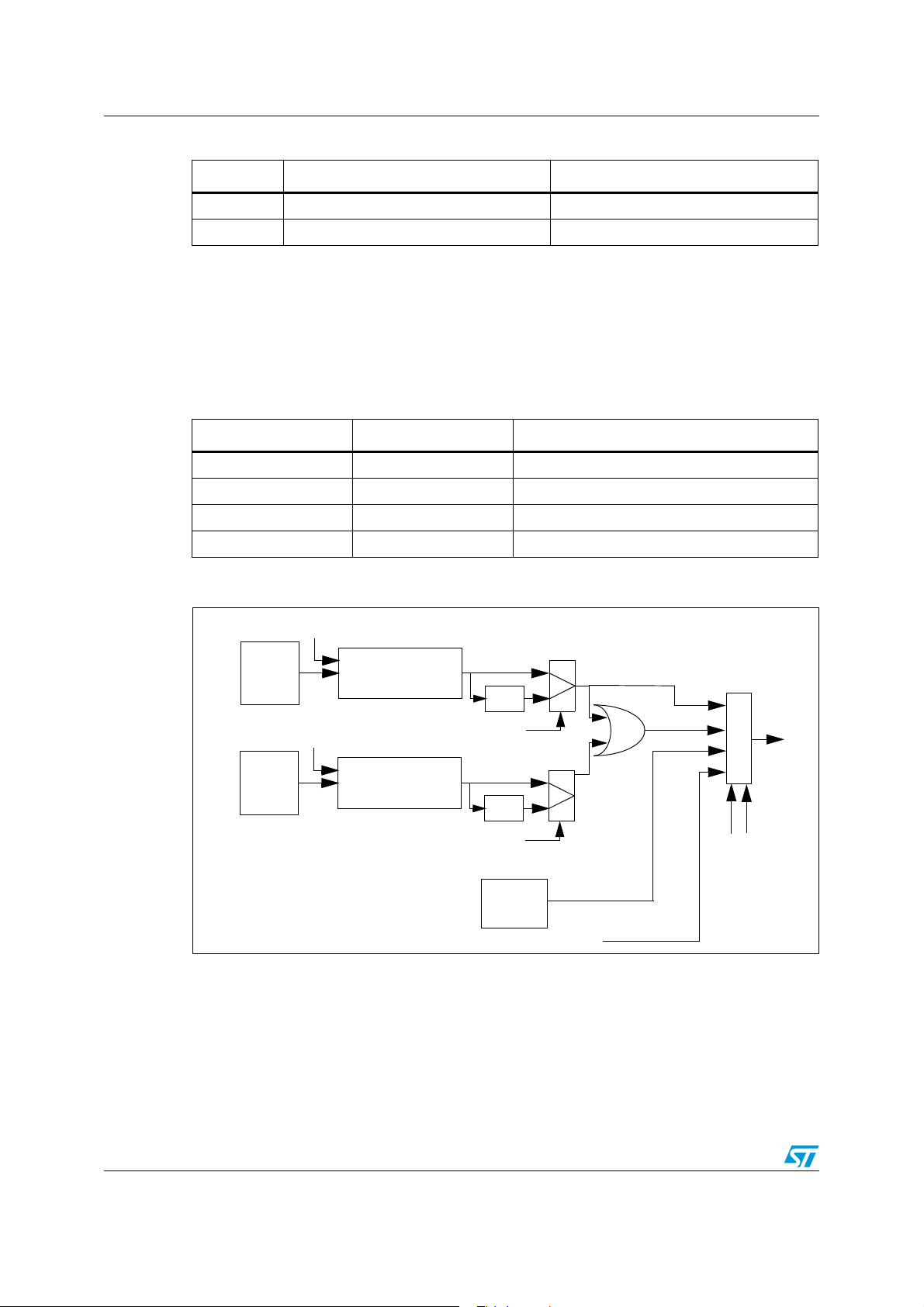
5.5 Free-fall detection
Free-fall detection refers to a specific configuration of the INTx_CTRL registers that allows
the recognition of device free-fall: the acceleration measurements along all the axes go to
zero. In real cases, a “free-fall zone” is defined around the zero-g level, where all
accelerations are small enough to generate the interrupt (Figure 11).
Doc ID 15136 Rev 2 25/31
Page 26

Interrupt generation AN2847
Figure 11. Free-fall interrupt
:
9
G
8
&&)NTERRUPT
&2%%&!,,
:/.%
!-V
This paragraph provides the fundamentals for using the free-fall detection feature. In
particular, the software routine which configures the device to detect and signal free-fall
events is as follows:
1 write 2Fh into CTRL_REG1
2 write 00h into CTRL_REG2 // High pass filter disabled
// Turn on the sensor, enable X, Y and Z
// ODR = 100 Hz
3 write 04h into CTRL_REG3 // Latched interrupt on INT1
4 write 16h into INT1_THS // Set free-fall threshold = 350mg
5 write 03h into INT1_DURATION // Set minimum event duration
6 write 95h into INT1_CFG // Configure free-fall recognition
7 poll INT1 pad; if INT1 = 0 then goto 8 // Poll INT1 pin waiting for the free-fall event
8
9 read INT1_SRC register // Clear interrupt request
10 goto 7
(Free-fall event has occurred; insert your
code here)
The code sample exploits a threshold set at 350 mg for free-fall recognition and the event is
notified by the hardware signal INT1. At step 5, the INT1_DURATION register is configured
to ignore events that are shorter than 3/DR = 3/100 ~= 30 ms in order to avoid false
detections.
Once the free-fall event has occurred, a read at
the device is ready to recognize other events.
5.6 6D direction
The LIS331DLH features an advanced capability to detect the orientation of the device in
space. The 6D direction function can be enabled through the AOI and 6D bits of the
INT1_CFG register (Table 3). When configured for the 6D function, the ZH, ZL, YH, YL, XH,
// Event handling
the INT1_SRC register clears the request and
26/31 Doc ID 15136 Rev 2
Page 27
AN2847 Interrupt generation
XL bits of INTx_SRC send information about the value of the acceleration generating the
interrupt when it exceeds the threshold, and whether the acceleration value is positive or
negative. More specifically:
● ZH (YH, XH) is 1 when the sensed acceleration is greater than the threshold in the
positive direction.
● ZL, (YL, XL) is 1 when the sensed acceleration is greater than the threshold in the
negative direction.
Figure 12. ZH, ZL, YH, YL, XH, XL behavior
&ULL3CALE
8(9(:(
4HRESHOLDMODULE
8(9(:(
GLEVEL
8,9,:,
4HRESHOLDMODULE
8,9,:,
&ULL3CALE
0OSITIVE
ACCELERATION
.EGATIVE
ACCELERATION
!-V
There are two possible configurations for the 6D direction function:
● 6D movement recognition: In this configuration the interrupt is generated when the
device moves from one direction (known or unknown) to a different, known direction.
The interrupt is active only for 1/ODR.
● 6D position recognition: In this configuration the interrupt is generated when the
device is stable in a known direction. The interrupt is active as long as the position is
maintained, as shown in Figure 13, (a) and (b).
In Figure 13, the 6D Movement line shows the behavior of the interrupt when the device is
configured for 6D Movement recognition on the X and Y axes (INT1_CFG = 0x4Ah), while
the 6D Position line shows the behavior of the interrupt when the device is configured for 6D
Position recognition on the X and Y axes (INT1_CFG = 0xCAh). INT1_THS is set to 0x21.
With reference to Figure 14, the device has been configured for the 6D Position function on
the X, Y and Z axes. Table 19 shows the content of the INT1_SRC register for each
position.
Doc ID 15136 Rev 2 27/31
Page 28

Interrupt generation AN2847
Figure 13. 6D movement vs. 6D position
$-OVEMENT
$0OSITION
8
9
A
:
Figure 14. 6D recognized positions
:
B
!-V
:
:
9
9
8
8
:
:
9
9
8
8
BA
:
:
9
9
:
:
9
9
8
9
:
:
4OP
4OP
28/31 Doc ID 15136 Rev 2
8
8
8
8
DC
:
9
9
"OTTOM
8
8
9
8
FE
!-V
Page 29

AN2847 Interrupt generation
Table 19. INTx_SRC register in 6D position
Case IA ZH ZL YH YL XH XL
(a)1000100
(b)1000010
(c)1000001
(d)1001000
(e)1100000
(f)1010000
Doc ID 15136 Rev 2 29/31
Page 30

Revision history AN2847
6 Revision history
Table 20. Document revision history
Date Revision Changes
26-Jan-2009 1 Initial release.
08-Sep-2010 2
Updated Table 5: Output data register content vs. acceleration (FS =
2 g).
30/31 Doc ID 15136 Rev 2
Page 31

AN2847
Please Read Carefully:
Information in this document is provided solely in connection with ST products. STMicroelectronics NV and its subsidiaries (“ST”) reserve the
right to make changes, corrections, modifications or improvements, to this document, and the products and services described herein at any
time, without notice.
All ST products are sold pursuant to ST’s terms and conditions of sale.
Purchasers are solely responsible for the choice, selection and use of the ST products and services described herein, and ST assumes no
liability whatsoever relating to the choice, selection or use of the ST products and services described herein.
No license, express or implied, by estoppel or otherwise, to any intellectual property rights is granted under this document. If any part of this
document refers to any third party products or services it shall not be deemed a license grant by ST for the use of such third party products
or services, or any intellectual property contained therein or considered as a warranty covering the use in any manner whatsoever of such
third party products or services or any intellectual property contained therein.
UNLESS OTHERWISE SET FORTH IN ST’S TERMS AND CONDITIONS OF SALE ST DISCLAIMS ANY EXPRESS OR IMPLIED
WARRANTY WITH RESPECT TO THE USE AND/OR SALE OF ST PRODUCTS INCLUDING WITHOUT LIMITATION IMPLIED
WARRANTIES OF MERCHANTABILITY, FITNESS FOR A PARTICULAR PURPOSE (AND THEIR EQUIVALENTS UNDER THE LAWS
OF ANY JURISDICTION), OR INFRINGEMENT OF ANY PATENT, COPYRIGHT OR OTHER INTELLECTUAL PROPERTY RIGHT.
UNLESS EXPRESSLY APPROVED IN WRITING BY AN AUTHORIZED ST REPRESENTATIVE, ST PRODUCTS ARE NOT
RECOMMENDED, AUTHORIZED OR WARRANTED FOR USE IN MILITARY, AIR CRAFT, SPACE, LIFE SAVING, OR LIFE SUSTAINING
APPLICATIONS, NOR IN PRODUCTS OR SYSTEMS WHERE FAILURE OR MALFUNCTION MAY RESULT IN PERSONAL INJURY,
DEATH, OR SEVERE PROPERTY OR ENVIRONMENTAL DAMAGE. ST PRODUCTS WHICH ARE NOT SPECIFIED AS "AUTOMOTIVE
GRADE" MAY ONLY BE USED IN AUTOMOTIVE APPLICATIONS AT USER’S OWN RISK.
Resale of ST products with provisions different from the statements and/or technical features set forth in this document shall immediately void
any warranty granted by ST for the ST product or service described herein and shall not create or extend in any manner whatsoever, any
liability of ST.
ST and the ST logo are trademarks or registered trademarks of ST in various countries.
Information in this document supersedes and replaces all information previously supplied.
The ST logo is a registered trademark of STMicroelectronics. All other names are the property of their respective owners.
© 2010 STMicroelectronics - All rights reserved
STMicroelectronics group of companies
Australia - Belgium - Brazil - Canada - China - Czech Republic - Finland - France - Germany - Hong Kong - India - Israel - Italy - Japan -
Malaysia - Malta - Morocco - Philippines - Singapore - Spain - Sweden - Switzerland - United Kingdom - United States of America
www.st.com
Doc ID 15136 Rev 2 31/31
 Loading...