

Page 1

AN2846
Application note
SCLT3-8 - guidelines for use in industrial automation applications
Introduction
The serial current limited termination device SCLT3-8 provides 8 inputs and supports the
data transfer of the input states through a limited opto-transistor count thanks to the digital
SPI (serial peripheral interface).
The purpose of this document is to:
■ Help designers to use the SCLT3-8 in basic operations and to allow them to use it easily
in their own applications by describing the SCLT3-8 behavior in detail (Refer also to the
SCLT3-8 device datasheet and to the User guide for the evaluation board
STEVAL-IFP000V1.)
■ Provide basic schematic diagrams
■ Provide information on the thermal behavior of the SCLT3-8 device
■ Offer recommendations to achieve robust SCLT3-8 designs to optimize EMI protection in
accordance with industry standards (IEC 61000-4-2, 4-4, 4-5 and 4-6)
February 2010 Doc ID 15130 Rev 1 1/35
www.st.com
Page 2

Contents AN2846
Contents
1 Application guidelines . . . . . . . . . . . . . . . . . . . . . . . . . . . . . . . . . . . . . . . 4
1.1 Features of the SCLT3-8 . . . . . . . . . . . . . . . . . . . . . . . . . . . . . . . . . . . . . . 4
1.2 Current-limited inputs . . . . . . . . . . . . . . . . . . . . . . . . . . . . . . . . . . . . . . . . . 5
1.2.1 Maximum input current setting . . . . . . . . . . . . . . . . . . . . . . . . . . . . . . . . . 5
1.2.2 Input characteristics (IEC 61131-2 standard) . . . . . . . . . . . . . . . . . . . . . 6
1.2.3 Digital input filter . . . . . . . . . . . . . . . . . . . . . . . . . . . . . . . . . . . . . . . . . . . 9
1.2.4 Input signal frequency limitation . . . . . . . . . . . . . . . . . . . . . . . . . . . . . . 10
1.2.5 Input state monitoring . . . . . . . . . . . . . . . . . . . . . . . . . . . . . . . . . . . . . . 11
1.3 Monitoring functions and regulator . . . . . . . . . . . . . . . . . . . . . . . . . . . . . . 11
1.3.1 VCC monitoring . . . . . . . . . . . . . . . . . . . . . . . . . . . . . . . . . . . . . . . . . . . 11
1.3.2 Power loss detection . . . . . . . . . . . . . . . . . . . . . . . . . . . . . . . . . . . . . . . 12
1.3.3 Overtemperature detection . . . . . . . . . . . . . . . . . . . . . . . . . . . . . . . . . . 12
1.3.4 Internal voltage regulator 5 V . . . . . . . . . . . . . . . . . . . . . . . . . . . . . . . . . 12
1.4 SPI functional description . . . . . . . . . . . . . . . . . . . . . . . . . . . . . . . . . . . . 13
1.4.1 Input state register and parity bit generator . . . . . . . . . . . . . . . . . . . . . 14
1.4.2 Data shift register and control shift register . . . . . . . . . . . . . . . . . . . . . . 15
1.4.3 Digital inputs and outputs . . . . . . . . . . . . . . . . . . . . . . . . . . . . . . . . . . . 15
1.4.4 SPI functionality . . . . . . . . . . . . . . . . . . . . . . . . . . . . . . . . . . . . . . . . . . . 17
1.4.5 SPI timing definition . . . . . . . . . . . . . . . . . . . . . . . . . . . . . . . . . . . . . . . . 18
2 Thermal dissipation calculation . . . . . . . . . . . . . . . . . . . . . . . . . . . . . . . 19
2.1 Forward inputs polarity case . . . . . . . . . . . . . . . . . . . . . . . . . . . . . . . . . . 19
2.2 Reverse polarity on a single input case . . . . . . . . . . . . . . . . . . . . . . . . . . 20
2.3 Temperature gradient on the SCLT3 and on the board . . . . . . . . . . . . . . 20
3 Application circuit . . . . . . . . . . . . . . . . . . . . . . . . . . . . . . . . . . . . . . . . . 22
3.1 Basic SCLT3-8 board description . . . . . . . . . . . . . . . . . . . . . . . . . . . . . . . 22
3.2 Component definitions . . . . . . . . . . . . . . . . . . . . . . . . . . . . . . . . . . . . . . . 23
3.2.1 Footprint . . . . . . . . . . . . . . . . . . . . . . . . . . . . . . . . . . . . . . . . . . . . . . . . . 24
4 Isolation management . . . . . . . . . . . . . . . . . . . . . . . . . . . . . . . . . . . . . . 25
4.1 Opto-coupler isolation . . . . . . . . . . . . . . . . . . . . . . . . . . . . . . . . . . . . . . . 25
4.2 Magnetic digital isolator . . . . . . . . . . . . . . . . . . . . . . . . . . . . . . . . . . . . . . 27
2/35 Doc ID 15130 Rev 1
Page 3

AN2846 Contents
5 SCLT3-8 link configurations . . . . . . . . . . . . . . . . . . . . . . . . . . . . . . . . . . 28
6 Electromagnetic compatibility (EMC) requirements . . . . . . . . . . . . . . 29
6.1 IEC 61000 4-2 . . . . . . . . . . . . . . . . . . . . . . . . . . . . . . . . . . . . . . . . . . . . . 29
6.2 IEC 61000 4-4 . . . . . . . . . . . . . . . . . . . . . . . . . . . . . . . . . . . . . . . . . . . . . 30
6.3 IEC 61000 4-5 . . . . . . . . . . . . . . . . . . . . . . . . . . . . . . . . . . . . . . . . . . . . . 32
6.3.1 Results on input pins . . . . . . . . . . . . . . . . . . . . . . . . . . . . . . . . . . . . . . . 32
6.3.2 Results on VC pin . . . . . . . . . . . . . . . . . . . . . . . . . . . . . . . . . . . . . . . . . 33
6.4 IEC 61000 4-6 . . . . . . . . . . . . . . . . . . . . . . . . . . . . . . . . . . . . . . . . . . . . . 33
7 Conclusion . . . . . . . . . . . . . . . . . . . . . . . . . . . . . . . . . . . . . . . . . . . . . . . . 34
8 Revision history . . . . . . . . . . . . . . . . . . . . . . . . . . . . . . . . . . . . . . . . . . . 34
Doc ID 15130 Rev 1 3/35
Page 4
Application guidelines AN2846
V
CS
V
DD
Input
state
register
Data
Transfer
logic
shift
register
Parity
bits
gen.
4 lines
8 lines
8
lines
8 lines
Prog.
digital
filters
8 Lines
Current
reference
Oscillator
Undervoltage
alarm
Power
reset
Power
supply
/CS
SPM
SCK
MOSI
/MISO
COM
S
MISO
V
C
DVR
OSC
REF
IN
1
LD
1
IN
8
LD
8
COM
P
V
DD
Overtemperature
alarm
Write
V
DD
Shift
Ctrl
shift
register
8/16
Bits
Shift
Input
protection
and
input current
limiters
MOSI
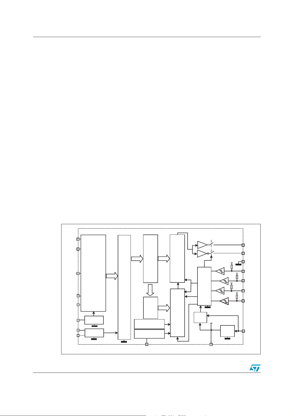
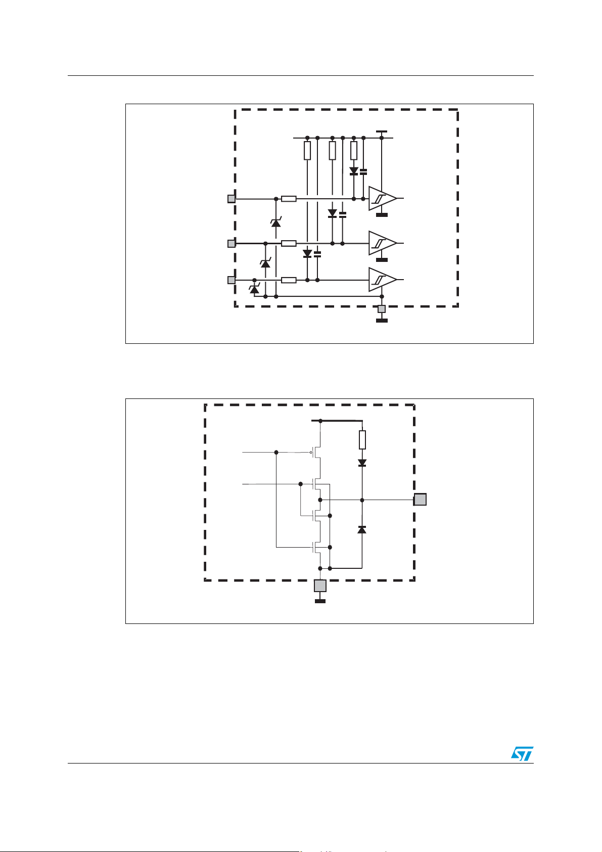
1 Application guidelines
1.1 Features of the SCLT3-8
The SCLT is an octal input active termination device designed for 24 V DC high density input
modules used in industrial automation. Each channel circuit terminates the connection
between a high side proximity sensor and the I/O module.
The advanced features of the SCLT3-8 compared to the basic CLT3-4BT6 device are:
● SPI for digital output count reduction
● Doubling of input terminations: 8 inputs compared to 4
● Input state monitoring by LEDs from the process section
● Undervoltage alarm detection of the power bus
● Power bus loss detection
● 5 V supply source available for external driving circuits like opto-couplers or magnetic
isolators
● Overtemperature detection
● Checksum data transmission through SPI for better data transfer integrity
The SCLT3-8 also features an input overvoltage protection. This input protection makes this
device robust against electromagnetic interference as defined in IEC 61000-4-x standards:
ESD, fast transient bursts, and voltage surges.
It is housed in a very low R
exposed pad, surface mount, HTSS0P38 package to reduce
TH
the circuit board size and the cooling pad.
Figure 1 shows the schematic block diagram for the device.
Figure 1. Schematic block diagram
Transfer
logic
Bits
4/35 Doc ID 15130 Rev 1
Page 5
AN2846 Application guidelines
The SCLT3-8 has been designed to run with SPI protocol C
format is 16 bits or 8 bits long according to SPM pin level. When SPM is grounded, 16 bits
are transmitted - 8 input data bits and 8 control bits. When SPM is connected to V
the 8 input data bits are transmitted.
Ta bl e 1 defines the significance of the16 bits. Bit 15 is the most significant bit. Detailed SPI
functionality is described in Section 1.4.
Table 1. 16-bit frame definition
Bit15 Bit14 Bit13 Bit12 Bit11 Bit10 Bit09 Bit08
Data bits
IN
8
IN
7
Bit07 Bit06 Bit05 Bit04 Bit03 Bit02 Bit01 Bit00
Control Bits
/UVA /OTA PC1 PC2 PC3 PC4 0 1
1.2 Current-limited inputs
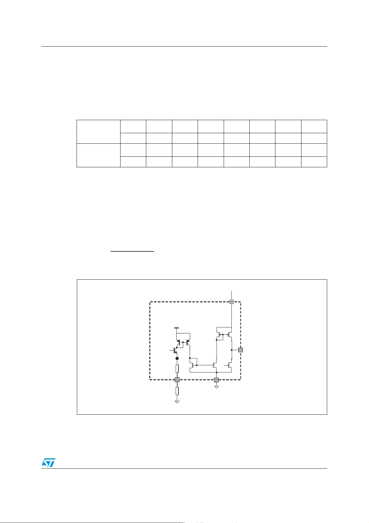
1.2.1 Maximum input current setting
All internal bias currents sources and particularly the input current limiter are defined by the
reference resistor connected to pin REF. A 15 kΩ resistor will assure a typical input limited
current of 2.35 mA (see Figure 2). The typical limited input current I
formula:
V
REF
BG
kR
5.1
+
I
LIM
30
·=
()
IN
= 0 and C
PHA
BG
IN
5
25.1Vcalwith typi
=
6
IN
4
IN
3
LIM
V
= 0. The frame
POL
DD
IN
2
is given by the
only
IN
1
Figure 2. Current limiter diagram
I
LIM
1 : 20
1 : 1
LED
VBG=1.25V
1.5k
REF
R
=15k
REF
2 : 3
LED_ON
COMs
The technology used allows a very low current dispersion according to the different
channels (less than 10%). The reference voltage V
is also compensated over the junction
BG
temperature range from -25 °C to 150 °C enabling a good stability of the limited current (see
Figure 3).
Doc ID 15130 Rev 1 5/35
Page 6
Application guidelines AN2846
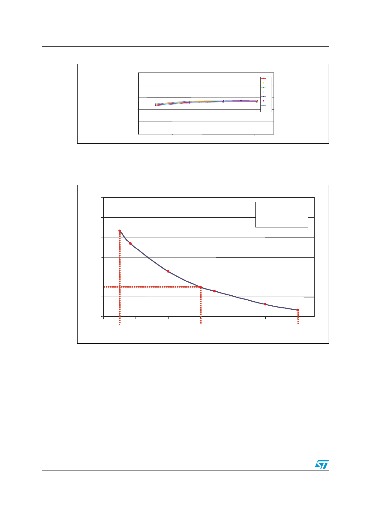
Figure 3. Limited current versus junction temperature
I (mA)
lim
2.6
2.5
2.4
2.3
2.2
2.1
-25°C 25°C 125°C 150°C
Vcc = 24 V, Vi = 11 V
Junction temp (°C)
IN1
IN2
IN3
IN4
IN5
IN6
IN7
IN8
Figure 4 shows the I
trend versus R
LIM
. according to the input current setting and
REF
therefore the dissipated power, the SCLT3-8 should be cooled with a sufficient copper heat
sink area (see Section 2)
Figure 4. Typical limiting input current versus R
I (mA)
lim
8.0
7.0
6.0
5.0
4.0
3.0
2.0
3 5 7 9 11 13 15
9.13.9
REF
Test conditions:
I versus R
LIM REF
V = 24 V, V = 24 V
CC I
R (k)
REF
15
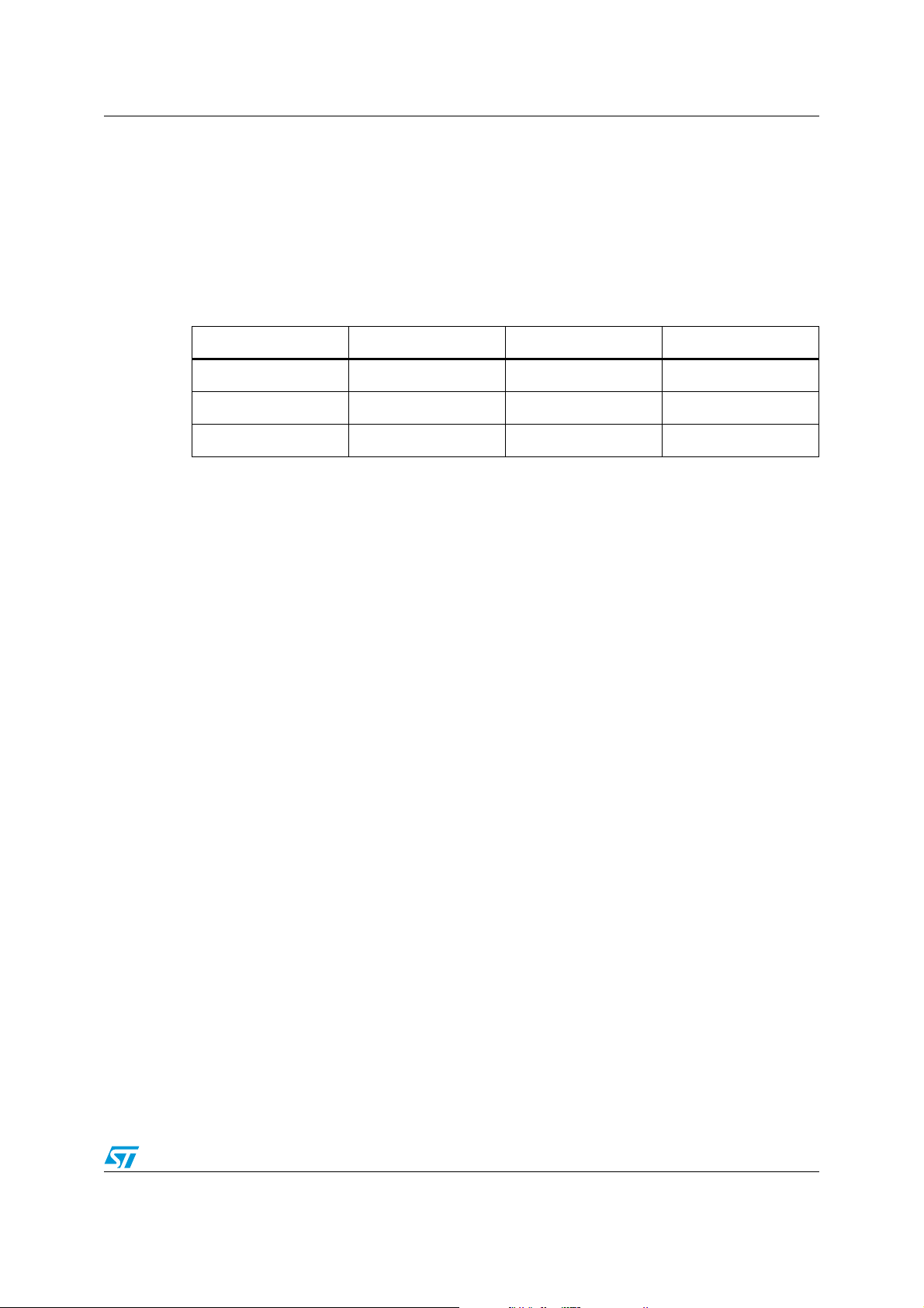
1.2.2 Input characteristics (IEC 61131-2 standard)
According to the IEC 61131-2 standard and referring to type 3, when the input current is less
than 1.5 mA the output circuit passes all the input current, keeping the monitoring LED off
and transmits a low level state to the input state register.
When the module input voltage V
than 11 V (that is, the SCLT3-8 input voltage V
on and the circuit transmits a high level state to the input state register.
Figure 5 gives the input characteristics and operating regions of type 3, defined in the
IEC 61131-2 standard, and the typical SCLT3-8 input characteristic.
6/35 Doc ID 15130 Rev 1
, taking into account the 2.2 kΩ input resistor, is higher
I
is higher than 5 V) the monitoring LED is
IN
Page 7
AN2846 Application guidelines
INPUT STATUS
Figure 5. Input characteristic according to IEC 61131-2 type 3
(V)
IN
V
11V
OFF Region
5V
0.1
Transition Region
OFF
OFF
ON Region
ON
ON
11V
SCLT3-8 (including RIN)
input characteristic
5V
OFF
I
2.01.5
I
LIMIT
(mA)
IN
Current limited inputs allow reduced power dissipation into the device as well as reduced
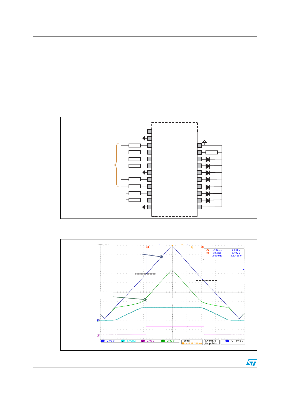
power needed by the external supplies. A typical application circuit schematic is shown in
Figure 31 in the application section.
Figure 6 displays the SCLT3-8 input stage configuration and its typical input threshold
voltages. Low frequency triangular waveform as the input voltage has been used to better
highlight the voltage thresholds. Input current (I
displayed in Figure 6. The V
wave shape shows clearly the on-off states of the SCLT3-8.
LED
) and voltage across the LEDs are also
IN
Figure 6. Input stage
VIN:
2V/div
VI: 2V/div
V
IN_ON
= 9.5 V
I
LIM
= 2.35 mA
V
IN_OFF
IIN: 1mA/div
=8.0 V
R
IN
V
I
IN
V
I
IN
V
LED
TH
2.35 mA
DIGITAL
FILTER
V
LED
Input stage configuration Typical input voltage thresholds
With R
= 2.2 kΩ, the typical V
IN
I_ON
and V
threshold voltages are respectively 9.5 V
I_OFF
and 8.5 V, consistent with the 11 V min. and 5 V max specified in the IEC 61131-2 standard.
The hysteresis (1 V) improves the input noise immunity.
The module input thresholds are the results of drop voltage across the input resistor R
into which flows the input current I
V
TH_OFF
.
The input current limiter is activated typically when V
, and the SCLT3-8 input thresholds V
IN
= 3.7 V, before the V
IN
TH_ON
TH_ON
and
threshold
,
IN
is reached.
In all cases the following formula can be applied:
VIRV+×=
INININI
When the input current limiter is activated, the formula becomes:
VIRV+×=
The typical module input threshold voltage can be calculated as follow:
VIRV
Math Composer 1.1.5
+×=
ONVTHILIMINONIN
__
Doc ID 15130 Rev 1 7/35
Page 8
Application guidelines AN2846
The proposed RIN value of 2.2 kΩ has been calculated to meet the IEC 61131-2 threshold
requirements. Users can set their own particular application threshold voltages by applying,
in the formula given above, the V
value. Take note, the higher the R
they want to achieve and find the corresponding RIN
IN
, the better will be the immunity against voltage surges.
IN
A particular useful application is when an input type 2 is needed. Figure 7 shows the
solution of connecting R
R
= 9.1 kΩ to get 3.5 mA (see Figure 4) in each input branch. Of course corresponding
REF
and input R
IN7
= 1.5 kΩ in parallel and tuning the I
IN8
LIM
with
bits (B14, B15) will be set together at the right state according to the level applied at the
common input. Unused LED outputs must be grounded to maintain the flow of the
current in its corresponding chanel.
Figure 7. IN
The different threshold voltages and the I
and IN8 parallel wired for type 2
7
RIN= 1.5k Ω
Type 3 inputs
Type 2 inputs
R
IN
1
IN
2
IN
3
IN
4
IN
5
IN
6
IN
7
IN
8
= 7.0 mA are shown in Figure 8 below.
LIMIT
R
REF
LED
LED
LED
LED
LED
LED
LED
LED
1
2
3
4
5
6
7
8
REF
= 9.1kΩ
Figure 8. Threshold voltages - type 2 configuration using two inputs in parallel
VI(2V/div)
V
= 9.9 V
I_ON
V
(2V/div)
(5mA/div)
I
IN
V
IN
LED
I
LIMIT
8/35 Doc ID 15130 Rev 1
= 7.0mA
V
I_OFF
= 8.4 V
Page 9
AN2846 Application guidelines
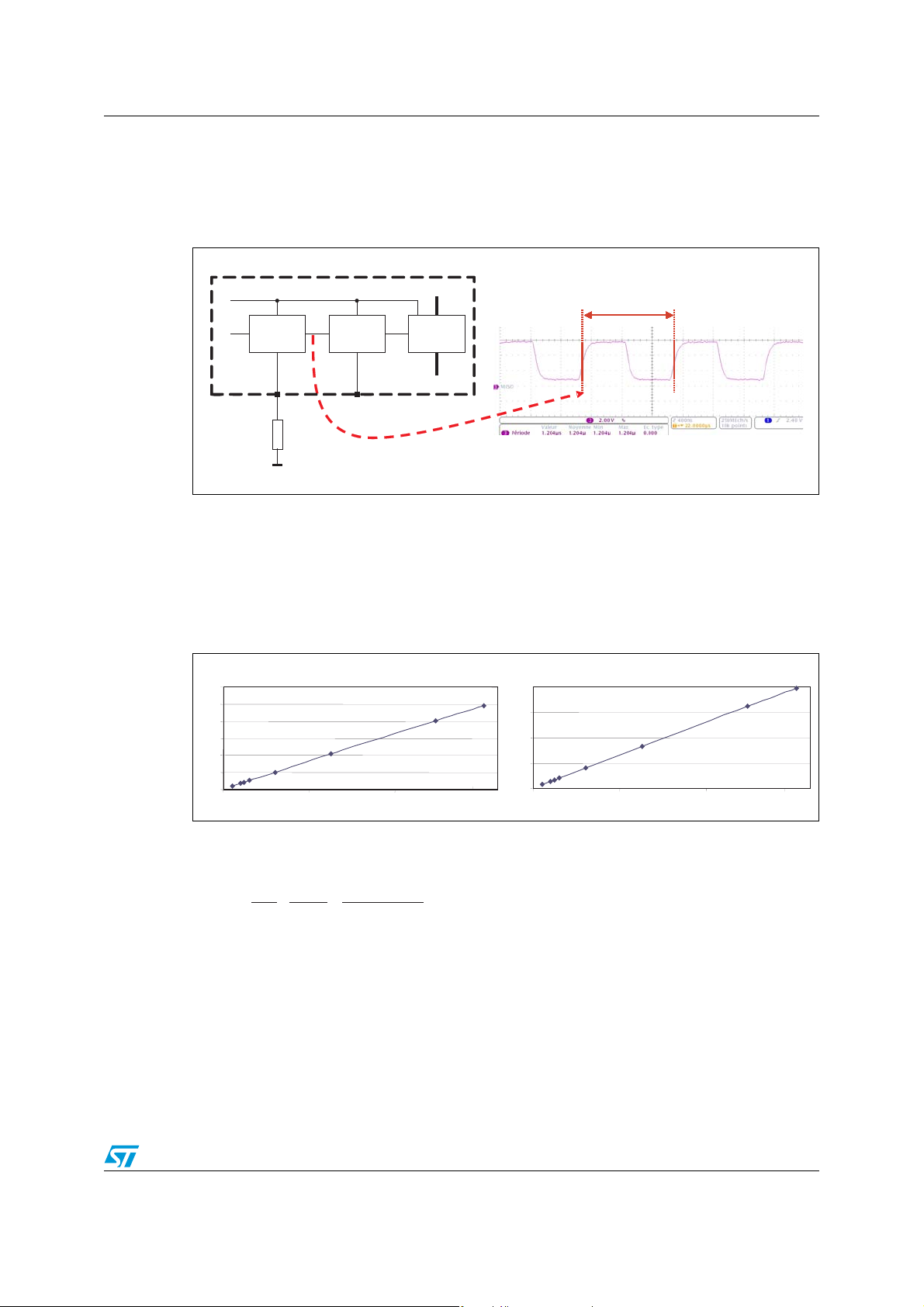
1.2.3 Digital input filter
Input parasitic disturbances can be removed by the programmable input digital filter. It is
based on an RC oscillator, a divider and a two step filter (see Figure 9).
Figure 9. Digital input filter.
CKF
IN<1:8>
OUT<1:8>
OSC period = 1.2 µ s
POR
REF1V
R
OSC
Oscillator
= 51 k
OSC
OSCR DVR
Divider filter_2step
The internal capacitor value is typically 10 pF. The oscillator resistor is connected externally
on pin R
when it is connected to V
least three rising edges as shown in Figure 9. The delay time is between 2 · t
3·t
OSC
. The clock divider is set at 8 when the pin DVR is connected to GND or at 64
OSC
. A wide filter time range, tFT, can be set by using the couple R
. The two step filter validates the input voltage when it sees at
DD
OSC
and DVR as
OSC
and
shown in below in Figure 10.
Figure 10. Minimum t
t (µS)
FT
600
500
400
300
200
100
0
0 500 1000 1500
FT
DVR=8
versus R
OSC
Rosc(k )Ω
t (µS)
FT
4000
3000
2000
1000
0
0 500 1000 1500
DVR=64
Rosc
(K )Ω
The user can also choose a particular typical filter time, tFT, by calculating the corresponding
R
value from the formula:
OSC
Math Composer 1.1.5
t
R
OSC
FT
2
××=
DVR
11
-
12
105.23
×
Doc ID 15130 Rev 1 9/35
Page 10
Application guidelines AN2846
1.2.4 Input signal frequency limitation
The maximum frequency transmitted trough the current limited inputs is limited by 3 factors:
1. The input digital filter, which cuts undesirable frequencies. R
DVR connected to GND ensures that the input signal has to be at a stable level for
more than 20 µs to be taken into account. This allows a maximum input frequency of
25 kHz. It can be reduced to 130 Hz using the combination of R
connected to V
2. The input capacitors C
signal. R
= 2.2 kΩ and CIN = 22 nF ensures a 3.2 kHz low pass filter.
IN
DD
.
are used to increase the EMI immunity filter of the input
IN
3. The SPI sampling effect - the input states are taken into account at each /CS fall (see
Section 1.4.4). This achieves a sampling of inputs at the /CS frequency, as shown in
Figure 11. The input states will be correctly transmitted if the sampling mode meets the
Shannon equation:
F2F
•=
InputCS/
Fwith
/CS
Input
1
=
t
/CS
=
/CS
frequencyinputmaxFwith
/CSthetwith:
periodsignal
Figure 11. Sampling effect
t
INPUT
set to 51 kΩ and
OSC
= 1.5 MΩ and DVR
OSC
Low level capture
missed
Current limited Input signal
/CS
High level capture
missed
t
/CS
As the /CS period is dependant on the frame length, Tab le 2 below gives some useful
combinations of SCK frequency signal, frame length and current limited input frequency.
Table 2. Input frequency versus SCK and length frame
F
SCK
Frame length 8 16 32 64 8 16 32 64 8 16 32 64 bits
t
/CS
F
current limited input
0.1 1.0 2.0 MHz
80 160 320 640 8 16 32 64 4 8 16 32 µs
6.25 3.125 1.56 0.78 62.5 31.25 15.6 7.8 125 62.5 31.25 15.6 kHz
10/35 Doc ID 15130 Rev 1
Page 11
AN2846 Application guidelines
1.2.5 Input state monitoring
The state of each of the 8 monitoring LEDs is an image of the 8 filtered input states. All the
monitoring LED cathodes have to be connected to ground. In the on state a current of I
reduced by 0.15 mA is available for each LED. In case of a LED not being used, the LED
output pin must be connected to the ground COM
to allow the input current to flow back to
P
the ground.
LIM
The LEDs must be chosen with a V
voltage less then 2.7 V (at minimum operating
F
temperature -25 °C).
1.3 Monitoring functions and regulator
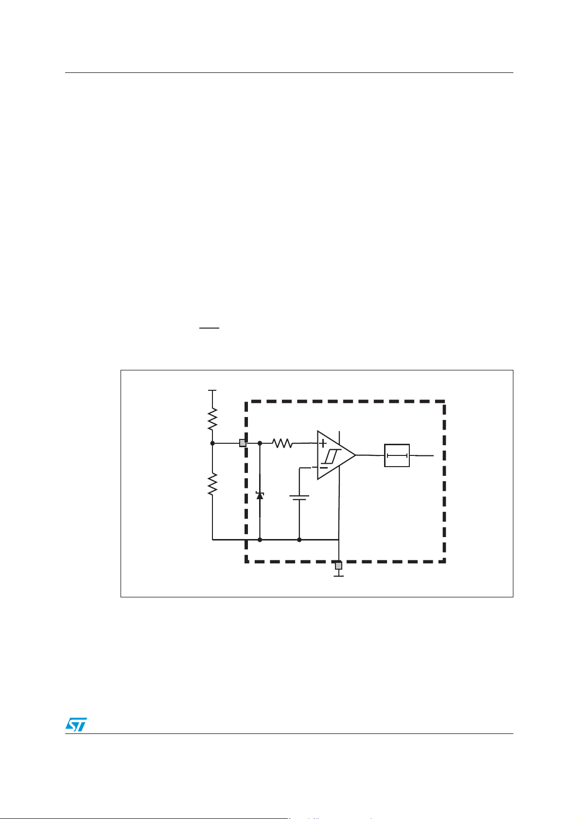
1.3.1 VCC monitoring
The power bus voltage connected to VCC is sensed by the VCS pin through a resistor bridge.
The V
easily set their own alarm detection voltage by an appropriate resistor bridge (see
Figure 12) using the formula:
Figure 12. UVA comparator
threshold voltage is typically 1.25 V with a hysteresis of 100 mV. Designers can
CS
R
VV+=
min_
CSCC
S
)1(
R
PD
V
CC
R
S
V
CS
V
DD
UVA
R
PD
VBG=1.25V
For example, the resistor bridge consisting of R
activation when V
drops below 17 V. The UVA activation has no effect on SCLT3-8
CC
COM
= 1.5 MΩ and R
S
1ms delay
= 120 kΩ produces UVA
PD
behavior but the information is transmitted trough the SPI bus by setting bit 7 to low state in
the control bits register (see Figure 13 and Figure 14).
To eliminate any short voltage disturbances that could trigger the UVA, a 1 ms delay circuit
has been inserted in the output line of the UVA comparator.
Doc ID 15130 Rev 1 11/35
Page 12

Application guidelines AN2846
Figure 13. V
MISO
MISO
SCK
SCK
/CS
/CS
= 24 V, UVA bit not activated Figure 14. VCC = 16 V, UVA bit activated
CC
VCC= 24 V
MISO
MISO
SCK
SCK
/CS
/CS
VCC= 16 V
1.3.2 Power loss detection
For a greater voltage drop on VC, a power supply loss detection has been added. This
immediately sets MISO output at low level state when V
Figure 15 and Figure 16. The MCU can then interpret that if all bits are equal to 0, this
means that V
is too low.
C
Figure 15. Communication stops for VC < 8 V Figure 16. Communication resumes for
is below 8 V, as shown in
C
V
> 8.1 V
C
V
C
/CS
SCK
MISO
8.0 V
MISO goes to L
1.3.3 Overtemperature detection
When the junction temperature exceeds 150 °C an overtemperature alarm sets the MISO
bit 6 at low state in the control bits register. The SCLT3-8 remains operational. The MCU
receiving the alarm has to take the corrective actions. The alarm will be reset when the
junction temperature falls below 135 °C.
1.3.4 Internal voltage regulator 5 V
The input of this voltage regulator is internally connected to the VC pin. The voltage
regulator supplies the digital part of the SCLT3-8 and therefore it defines the high digital
level. It also supplies the sourced current available at pin MISO. It can also supply
application needs (such as opto-couplers and micro transformers) through pin V
current capability is 9 mA for a 3% voltage drop on V
/CS
SCK
MISO
(see Figure 17).
DD
8.1 V
. Its total
DD
12/35 Doc ID 15130 Rev 1
Page 13

AN2846 Application guidelines
Figure 17. Regulator output voltage
V versus I
5.1
5.0
4.9
4.8
4.7
4.6
4.5
V (V)
dd
dd dd
V -3%
dd
I (mA)
dd
9.0
Figure 18 shows the schematic diagram of a solution for applications where greater current
is needed. The bypass transistor allows extra current while maintaining a 5 V regulated
voltage (see Figure 19).
Figure 18. V
V
CC
SMAJ30A
booster schematic Figure 19. Load regulation with V
DD
R
2N2907A
E
R
C
I
RC
V
C
V
CS
IN
1
IN
2
IN
3
IN
4
SCLT3
R
LED
LED
LED
V
REF
DD
1
2
3
I
DD
VV
DD
V (V)
DD
5.100
5.050
5.000
4.950
4.900
4.850
4.800
0.00 5.00 10.00 15.00 20.00 25.00
0.00 5.00 10.00 15.00 20.00 25.00
V
booster
DD
DD
I (mA)
DD
The proposed circuit allows a 25 mA current load capability with a VDD regulation <2%. An
additional input protection device, like SMAJ30A, is needed to comply with voltage surges
because R
has to be reduced to limit the voltage drop across it.
C
The dissipated power in the bypass transistor PZT2N2907A is 550 mW.
Components used:
● PZT2N2907A (SOT223 with 1 cm
● R
= 330 Ω (1/8 W), RE = 51 Ω (1/8 W)
C
1.4 SPI functional description
Three registers (refer to Figure 1) are used to transfer input data and control data to the
16-bit data frame. The data frames are transmitted through four interface signals: /CS, SCK,
MOSI, and MISO.
Doc ID 15130 Rev 1 13/35
2
copper area)
Page 14

Application guidelines AN2846
∑
1N8 1N7 1N6 1N5 1N4 1N3 1N2 1N1
1
0 0
1 1
0 0
1
From
input
state
filter
1.4.1 Input state register and parity bit generator
After filtering, the 8 input termination states are stored in an 8-bit input state register. Its
content is an image of the filtered input states in real time.
Figure 20. Input state register and parity bit generator.
Filtered
Input
states
The SCLT3-8 has been designed to help diagnose incorrect data transmission. The four
parity bits generated by the parity bit generator are computed according to the input states
register content. They are updated each time the input state register content changes.
8 lines
Input state register
Parity
bits gen.
The parity bit 5 of PC1 register controls the 1 to 8 input data states; PC2-bit 4 controls inputs
5 to 8: PC3-bit 3 controls inputs 1 to 4;PC4-bit 2 controls inputs 3 to 6 according to the logic
equation:.
http://www.mathcomposer.com
n
INPUTstate
== odd.if0even,if1PC
See example in Figure 21.
The decoding of all the parity bit results will help the microcontroller detect the possible
corrupted pair of bits occurring during the transmission.
Figure 21. Parity bit generation example.
From
input
8 lines
state
filter
Input state register
8 lines
Parity
Bbits gen.
PC1
PC2
1
2
PC3
3
PC4
4
14/35 Doc ID 15130 Rev 1
Page 15

AN2846 Application guidelines
1.4.2 Data shift register and control shift register
Data and control shift registers are each 8 bits long. At each /CS falling edge all the data is
frozen and the 8 bits of the input states register are transferred to the data shift register (bits
8 to 15) while the control bits, consisting of four parity bits, overtemperature alarm bit,
undervoltage alarm bit and the stop bit, are transferred to the control shift register (bit 0 to
7).
The two last bits (bit 1 and bit 0) are always set respectively to 0 and 1 indicating the end of
data frame except in power loss case where all bits are set to 0.
Bit 15 will be the MSB and Bit 0 the LSB.
Figure 22. Data and control data shift registers.
8 Lines
Overtemperature
alarm
1.4.3 Digital inputs and outputs
These digital pins are involved with the SPI:
● /CS: Chip select input
● SCK: Serial clock input
● MISO: Master-in slave-out output
● /MISO: complementary MISO state
● MOSI: Master-out slave-in input (connected to ground when not used)
To improve the immunity of the digital inputs against noise, the digital inputs /CS, SCK and
MOSI have been designed to use a Schmitt trigger configuration. Each input is connected to
V
through a high impedance pull up resistor to set the input at high level state when no
DD
input signal is applied. Protection diodes are inserted with these pull-up resistors to prevent
the ESD reaching the V
. The digital input diagram is given in Figure 23.
DD
Input state register
8 lines
4 lines
Parity
bits gen.
Data shift register
Control shift register
Undervoltage
alarm
Doc ID 15130 Rev 1 15/35
Page 16
Application guidelines AN2846
Figure 23. Digital inputs diagram.
V
DD
/CS
SCK
MOSI
COM
S
The digital output signal MISO is delivered through a high-Z impedance buffer able to
source or sink 3 mA.
Figure 24. Digital output MOSI
UVA
EN
M1
M2
V
DD
COMCOM
MOSI
S
16/35 Doc ID 15130 Rev 1
Page 17

AN2846 Application guidelines
1.4.4 SPI functionality
At the /CS falling edge the following operations are done:
● The input data states, parity and control bits are frozen and stored in the data and
control shift registers.
● The MSB (Bit 15) is shifted out first to MISO.
The SCLT3-8 data transfer uses SPI protocol with C
POL
= 0, C
= 0 conditions. This
PHA
means the SCK signal must be at low level state when the /CS is falling (communication
starts). In this case the MSB (bit15) is transferred first from MISO as soon as /CS falls, and
all the remaining bits are transferred at each SCK falling edge.
Figure 25. SCK and /CS synchronization security
/CS
/CS
SCK
SCK
MISO
MISO
Bit14
SCK is low when /CS falls
/CS
SCK
MISO
Bit14
SCK is high when /CS falls
For more flexibility the SPI protocol has been enhanced and takes into account the case
where SCK signal is at high level when /CS falls to low level. In this case, as previously the
MSB will be present at MISO pin at the /CS falling edge but the following bit will be available
only at the second SCK falling edge.
In both cases the rule is: a rising SCK edge must occur after the falling /CS edge to validate
the first SCK falling edge. Otherwise the state change duration of MISO may be too short to
correctly trigger the transmission of the MSB (bit 15) (see Figure 25).
In normal operation the two last bits are 0 and 1 indicating the end of the transmission.
The data transmission runs as long as the /CS is at low state. As soon as /CS returns to
high level, the data transfer is disabled and the MISO output is in high impedance - hi-Z.
When MOSI input is used in daisy chain operation, the inputs are captured at each SCK
rising edge and loaded into the shift register. Loaded data has no effect on the SCLT3-8.
Figure 26. 16-bit transmission example
/CS
SCK
MISO
10 1 01111111 0110110 1 01111111 01101
B15 B8 B7 B0
Input data bits Control bits
Doc ID 15130 Rev 1 17/35
Page 18

Application guidelines AN2846
Figure 26 shows a 16-bit transmission example when the application is running in good
conditions:
● Application is correctly supplied: /UVA, Bit 7 not activated
● SCLT3-8 junction temperature less than 150 °C: /OTA, bit 6 not activated
● Correct transmission: parity bits in accordance with input states
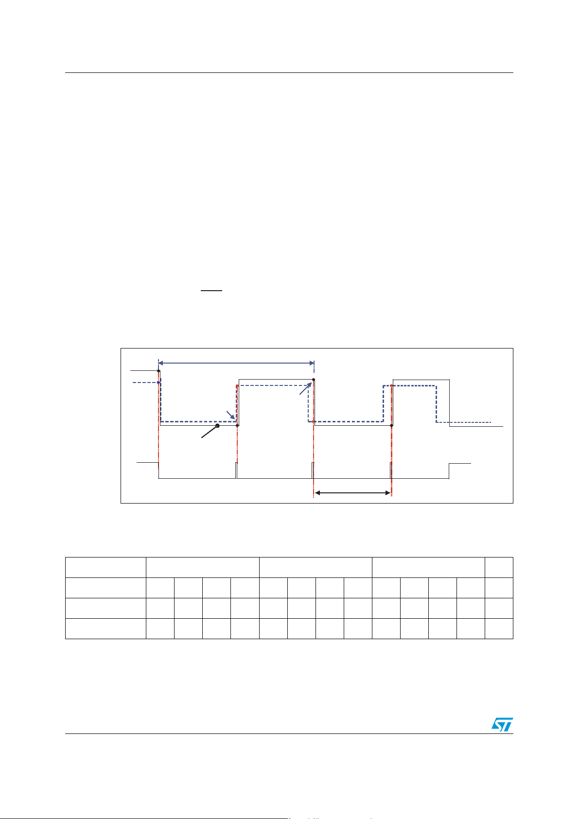
1.4.5 SPI timing definition
The four SPI signals involved: /CS, SCK, MOSI, MISO are described in Figure 27. A fifth
/MISO pin output signal is also present.
The typical SCK frequency is 1 MHz, but the SCLT3 can run at up to 2 MHz. The other more
important timing parameters are:
● t
: Delay time. This is the delay time of MISO between SCK falling edge and MISO
D
change.
● t
: Set up time. This is the minimum holding time of MOSI input data for its capture
S
before the SCK rising edge.
● t
: Holding time. This is the minimum holding time of MOSI input data after the SCK
H
rising edge for its correct capture.
The most important rules to meet to perform a correct data transmission are:
● t
● t
> tD + tS
CL
> tH.
CH
Figure 27. SPI timing definition.
/CS
SCK
MISO
MOSI
t
LD
t
A
12 16
t
t
D
MSB
S
t
C
t
DT
t
CL
CH t
t
t
S
H
LSB
HC
t
DIS
S
MSB
M
18/35 Doc ID 15130 Rev 1
Page 19

AN2846 Thermal dissipation calculation
2 Thermal dissipation calculation
2.1 Forward inputs polarity case
In reference to the application schematic defined in Figure 31, the dissipated power into the
SCLT3-8 P
Consider the worst case where all inputs are connected to 30 V.
P
= P1 - P2
SCLT
where:
P1 is the total power delivered by the supplies
P2 is the total power dissipated by the external components
can be calculated as following:
SCLT
P1 = V
External components are: R
Power dissipated by input resistors = 8 · R
· (IC + IDD + 8 · I
CC
)
LIM
, RC, LEDs, regulator load
IN
IN ·ILIM
2
Power dissipated by supply resistor = RC · (IC + IDD)2
Power dissipated by LEDs = 8 · V
Power supplied by the VDD linear regulator = V
The P
= 560 mW
SCLT
LED
· I
LED
REG
· I
DD
Assuming:
V
= 30 V, I
CC
= 2.35 mA, RIN = 2.2 kΩ, RC = 1.0 kΩ, V
LIM
LED
Note: The current flowing through the LED is almost the same as I
125 µA used to bias the input circuit device.
With the above mentioned conditions and using copper area of 1cm
SCLT3-8 junction temperature will be around 120 °C with an ambient temperature of 85 °C.
Figure 28 below shows the R
variations versus the heat sink area on a 35 µm FR4
TH_JA
epoxy single side board.
Figure 28. R
versus copper area
TH_JA
R (°C/W)
th(j-a)
120
HTSSOP38
= 2 V, VDD = 5 V, IDD = 7MA.
. The difference is about
LIMIT
2
as heat sink, the
SCLT
100
80
60
40
20
0
0 20 40 60 80 100 120 140 160 180
S (mm²)
Doc ID 15130 Rev 1 19/35
CU
Page 20

Thermal dissipation calculation AN2846
2.2 Reverse polarity on a single input case
Each input resistor can be connected to a reverse polarity down to -30 V. This case
corresponds to a connection mistake or a reverse biasing that is generated by the
demagnetization of a monitored inductive solenoid. The involved input can withstand a high
reverse current up to 20 mA. The corresponding state transmitted is low level. The other
inputs remain operational.
The power dissipated into a reverse polarized input is low, but attention has to be paid to
power dissipation into the input resistor which sustains almost all the reverse voltage.
2
P
dis_RIN
dis_RIN
()
=
7.0
-
V
I
R
IN
30
VP
ININ
Ω=-==
k2.2RandVformW390
2.3 Temperature gradient on the SCLT3 and on the board
Figure 29 shows the case top temperature when SCLT3-8 dissipates 600 mW, which
corresponds to maximum supply case with V
is 100 mm
2
, and the ambient temperature is 25 °C. In this example the maximum case top
temperature reaches 68 °C. The case top temperature is a good indication of the junction
temperature, which can be estimated using thermal analysis techniques.
and all module inputs at 32 V. The heat sink
CC
Figure 29. Case top temperature
R = 1.1 k
R = 2.2 k
Lens: G1
(Board paint in black)
Ω
C
IN
Ω
20/35 Doc ID 15130 Rev 1
Page 21

AN2846 Thermal dissipation calculation
Figure 30 shows the temperature gradient of the SCLT3-8 board with the same supply
conditions as above. Almost the totality of the power is concentrated around the SCLT3-8
and its heatsink. No particular temperature hot spot can be detected on the board.
Figure 30. Temperature gradient of the board
Profil 1Profil 1
Profil 1Profil 1
Doc ID 15130 Rev 1 21/35
Page 22

Application circuit AN2846
3 Application circuit
3.1 Basic SCLT3-8 board description
The basic electrical schematic diagram using a single SCLT3-8 fulfills the requirements
defined in the IEC 6131-2 standard. It is easy to duplicate this configuration to meet more
complex applications using many inputs and several SCLT3-8s.
The major settings are:
● Type 3 configuration
● 16-bit frame (SPM grounded)
● 16 µs digital input filtering (R
Figure 31. Type 3 application diagram
51k
33n
1.0k
1.5M
120k
22n
2.2k
22n
2.2k
22n
2.2k
J1
2.2k
2.2k
2.2k
2.2k
2.2k
22n
22n
22n
22n
DVR
OSC
SPM
COM
V
C
V
CS
COM
IN
IN
IN
IN
COM
IN
IN
IN
IN
COM
SCLT3-8
= 51 kΩ, DVR grounded)
OSC
V
DD
P
/CS
SCK
MOSI
P
1
2
3
4
P
5
6
7
8
P
/MISO
MISO
COM
R
REF
LED
LED
LED
LED
LED
LED
LED
LED
S
1
2
3
4
5
6
7
8
33n
10n10n
15k
220
220
470p
470p
J2
22/35 Doc ID 15130 Rev 1
Page 23
AN2846 Application circuit
3.2 Component definitions
The reference resistor R
tolerance gives the accuracy of the input limiters. 1% accuracy
REF
is suggested.
The typical type 3 SCLT3-8 application uses R
= 15 kΩ and RIN = 2.2 kΩ. Type 2 can be
REF
also achieved as shown in Tab le 3 .
The input MELF resistors are used to sustain high voltages occurring during surge tests.
Table 3. Type 2 and 3 configurations
Typ e 3 Type 2 Un it
R
REF
R
IN
Typical I
LIMIT
Using type 2, the power dissipated by the SCLT3-8 reaches 1W with VI = VCC = 24 V. A
copper heat sink area of 1 cm
The R
value has to be chosen with attention. The voltage drop across this resistor is the
C
15 3.9 kΩ
2.2 0.75 kΩ
2.3 6.5 mA
2
will set TJ at 150 °C with an ambient temperature of 65 °C.
product of SCLT3-8 supply current and any load current supplied by VDD: regulator output
current and sourced MISO current. The resulting voltage V
must be in any case above the
C
8 V activation threshold to avoid a spurious power loss detection. 1 kΩ meets this
requirement and allows 2 kV of voltage surge.
The 22 nF input capacitors are used to improve the noise immunity of the whole module.
Their function is to filter the high frequency electrical noise, and to secure the off state of the
module.
Adding a 33 nF capacitor on V
pin ensures high immunity against electrical noise such as
C
that described in the IEC 61131-2 standard.
R
= 51 kΩ and pin DVR grounded set the input digital filter to eliminate pulse widths
OSC
below 20 µs.
A 33 nF capacitor connected on V
output ensures a good output of the voltage regulator.
DD
The LEDs must be chosen according to their input diode drop voltage. LED outputs can
drive LEDs with forward voltage up to 2.7 V.
Low pass RC filters have been inserted into digital inputs /CS and SCK to improve the
immunity against fast transient bursts. R = 220 Ω and C = 470 pF give a good compromise
between immunity result and SCLT-3 speed which can run up to 1 MHz.
Doc ID 15130 Rev 1 23/35
Page 24

Application circuit AN2846
3.2.1 Footprint
The footprint given in Figure 32 allows ground connection optimization of COMP and
COMP
Figure 32. Foot print (not to scale)
. The 1 cm2 heat sink area defines an R
S
TH-JA
of 80 °C/W.
8.80
0.65
1.35
0.6
Pin 1
Package footprint
2.575
6.10
0.4
5.00
11.35
0.25
3.425
1.30
S
= 100 mm
COPPER
Copper thickness : 35
3.50
0.6
Additional copper for extra-cooling
²
µm
24/35 Doc ID 15130 Rev 1
Page 25

AN2846 Isolation management
4 Isolation management
There are two solutions proposed for galvanic isolation between the SCLT3-8 and the
microcontroller.
● Opto-coupler isolation
● Magnetic digital isolation
4.1 Opto-coupler isolation
The first solution is given by opto-couplers which must run at a bit rate compatible with the
SCK frequency and meet SCLT3-8 requirements in terms of consumption.
HCPL4506 or HCPL0466 can be a solution to drive a single SCLT3-8 for a 1 MHz
application.
Figure 33. Single SCLT3-8 and HCPL4506 or 0466
V
DD
Ω
3k
V
CC
V
C
/CS
SCK
MOSI
/MISO
MISO
1 k
If several SCLT3-8s are used, more current is available through V
couplers. The different outputs V
can be tied together but, low serial resistors (22 Ω) must
DD
Ω
3k
Ω
HCPL4506
or 0466
750
750
V
DD2
3 k
DD
Ω
/CS
Ω
SCK
Ω
MISO
pins to supply the opto-
be inserted to balance the different regulated output voltages. The load current is shared
between the two SCLT3s and allows the voltage drop reduction across each R
resistor.
C
Doc ID 15130 Rev 1 25/35
Page 26

Isolation management AN2846
Figure 34 shows two SCLT3s in daisy chain configuration using ACPL-K73L (dual) and
ACPL-W70L (single).
Figure 34. Two daisy-chained SCLT3-8s and ACPL/K73L/W70L
V
V
DD
22
ACPL-K73L
750
750
ΩΩ
/CS
Ω
SCK
/CS
V
V
CC
V
V
CC
V
V
C
V
V
C
/CS
SCK
SCK
MOSI
MOSI
/MISO
/MISO
MISO
MISO
V
V
DD
/CS
/CS
SCK
SCK
MOSI
MOSI
/MISO
/MISO
MISO
MISO
22
1 k
Ω
V
DD2
Ω
MISO
HCPLK73L
HCPW70L
26/35 Doc ID 15130 Rev 1
ACPL-W70L
Page 27

AN2846 Isolation management
4.2 Magnetic digital isolator
The second solution is given by digital isolators. The triple-channel digital isolator
ADUM1301 is convenient for such an SCLT3-8 application. The sending channels V
V
are used for /CS and SCK signals while receiving channel VIC is used for MISO signal.
IB
The V
pin of SCLT3-8 can easily deliver the typical supply current needed by V
DD
is around 2.7 mA at 2 MHz as shown in Figure 35.
Figure 35. Digital isolator
V
V
DD
/CS
V
V
CC
V
V
C
/CS
SCK
SCK
MOSI
MOSI
/MISO
/MISO
MISO
MISO
V
DD
GND
VOA
VOB
VIC
NC
VE
GND
V
2
2
DD
GND
VIA
VIB
VOC
NC
2
2
VE
GND
DD2
1
1
1
1
and
IA
, which
SCLT3 -8
SCLT3 -8
ADuM1301
Doc ID 15130 Rev 1 27/35
Page 28

SCLT3-8 link configurations AN2846
5 SCLT3-8 link configurations
Parallel and daisy chain configurations can be implemented using SCLT3-8 or other devices
compatible with a serial peripheral interface.
In parallel mode the microcontroller selects the SCLT-8 with which it wants to communicate
by setting the corresponding /CS to low state as long as the communication lasts. The
microcontroller should be able to control as many /CS pins as SCLT-8s it wants to address.
While in daisy chain configuration the microcontroller commands at the same time all the
SCLT3-8s connected in series. The data must transit from SCLT3-8 to SCLT3-8 going out
from the MISO pin, going in through MOSI pin till reaching the last one connected to the
microcontroller. Considering n SCLT3-8s connected in daisy chain, the microcontroller has
to read n times 16 bits and the communication time is proportional to n times 16 bits.
Figure 36. Daisy-chain configuration Figure 37. Parallel configuration
MASTER SPI
SCK
MISO
MOSI
/CS
SCLT
SCK
MISO
MOSI
/CS
SCLT
SCK
MISO
MOSI
/CS
1
2
MASTER SPI
SCK
MISO
MOSI
/CS1
/CS2
SCLT
SCK
MISO
MOSI
/CS1
SCLT
SCK
MISO
MOSI
/CS2
1
2
28/35 Doc ID 15130 Rev 1
Page 29

AN2846 Electromagnetic compatibility (EMC) requirements
6 Electromagnetic compatibility (EMC) requirements
The SCLT3-8 has been designed to withstand electromagnetic interference as specified in
the IEC 61131-2 standard. This international standard gives all the requirements and
conditions for tests that must be performed on the programmable logic controllers (PLC) and
their associated peripherals. IEC 61000 4-2, 4-4, 4-5 and 4-6 standards define test
methods.
The current limited inputs and supply pins of SCLT3-8 are protected against high voltage
disturbances by a clamping circuits that are grounded to the common pin COM
with serial input resistances R
or RC (see Figure 38). These clamping circuits are effective
IN
against ESD (±8 kV contact), fast transient burt (±2.5 kV), and voltage surge (±1 kV).
Figure 38. Protection clamping circuits
R
IN
IN
1
IN
V
CC
V
C
Supply
39V
circuit
COM
P
COM
S
IN
IN
IN
IN
IN
IN
39V
2
39V
3
39V
4
39V
5
39V
6
39V
7
39V
8
39V
. Combined
P
Input
circuit
6.1 IEC 61000 4-2
This standard specifies the behavior of the device when subjected to electrostatic
discharges. The discharges must be applied to operator accessible parts. This means that
these tests have to be performed on each connector pin. The required levels are: air
discharge: ±15 kV, contact discharge: ±8 kV.
The system must continue to operate as intended after the discharge. Temporary
degradation of the performance is acceptable during the test, but the system must recover
by itself after the test (B criterion).
All SCLT3-8 pins are ESD protected.
COM
P
COM
S
Doc ID 15130 Rev 1 29/35
Page 30

Electromagnetic compatibility (EMC) requirements AN2846
6.2 IEC 61000 4-4
This standard specifies the behavior of the device when subjected to a fast transient burst.
The fast transient burst must be applied on all the input pins of the system. A capacitive
clamp-coupling device is used as described in the IEC 61000-4-4 standard. The required
sustainable burst voltage level is 2.5 kV. The system must continue to operate as intended.
No temporary degradation of the performance is acceptable during the test (A criterion).
New test methodology has been set up to check the frame integrity against fast transient
bursts. The need to monitor each bit level leads to using a scope isolated from the test
bench through optic fibers. The generation of /CS and SCK input signals are also isolated
through the same way as shown in Figure 39. Current and voltage level adaptation is done
through an optical fiber interface (OFI).
Long frames history can be stored in the monitoring scope for an easier detection of
disrupted bits.
The SCLT3-8 immunity has been increased by adding RC filter networks connected on /CS
and SCK input pins. But these RC filters act as low pass filters and limit the maxim data
transfer speed. For example the filter made of R = 220 Ω, C = 470 pF allows a 1 MHz
transmission frequency and ensures device FTB immunity up to 4 kV.
Table 4. Speed - FTB immunity compromise
RC Values SCK speed FTB immunity
220 Ω - 220 p
F 2 MHz 3 kV
220 Ω – 470 pF 1 MHz 4 kV
The test configuration is shown in Figure 39.
Figure 39. Two supplies configuration
Bat
FTB
generator
Bat
2
Capacitive clamp
SCLT3-8
1
/CS
SCK
MISO
OFI
/CS
SCK
MISO
Fiber optic cable
OFI
Generator
/CS
SCK
MISO
Scope
30/35 Doc ID 15130 Rev 1
Page 31

AN2846 Electromagnetic compatibility (EMC) requirements
Figure 40 shows the output MISO behavior is not disturbed during fast transient bursts. The
FTB signal has been captured through an antenna to observe where the bursts act.
Figure 40. Output MISO behavior during fast transient bursts
+ 4.0 kV
CS
/SCK
FTB
MISO
FTB 200 µs = 5 kHz
=
Figure 41. Test bench
HAEFELY
Bat2
FTB generator
Capacitive cl amp
SCLT3 board
Bat1
SCLT3 inputs, Gnd
OFI
Fiber
optic
cable
Doc ID 15130 Rev 1 31/35
Page 32

Electromagnetic compatibility (EMC) requirements AN2846
6.3 IEC 61000 4-5
This standard specifies the behavior of the device when subjected to voltage surges applied
on all input pins of the system. For all analog inputs, the coupling method is a 42 Ω serial
resistance and a 0.5 µF capacitor. For the DC power line, the coupling is 2 Ω resistor, and
18 µF capacitor. The required voltage surge levels are:
● 1 kV for the input pins with R
● 2.5 kV for the pin V
when RC = 2.2 kΩ or 1 kV when RC = 500 Ω.
C
The system must continue to operate as intended. Temporary degradation of the
performance is acceptable during the test, but the system must recover by itself after the
test (B criterion).
6.3.1 Results on input pins
When a positive surge voltage of 1 kV is applied on the input resistor RIN, the input active
clamp protects the SCLT3-8 input and limits the input voltage at 40 V. The input current
reaches 0.45 A.
When a negative voltage surge is applied the input diode is biased in forward mode and the
current is 0.45 mA (see Figure 42)
= 2.2 kΩ,
IN
Figure 42. V
+ 1.0 kV
V
surge
0.2kV/div
I
IN
0.2A/div
V
IN
20V/div
Positive voltage surge
and IIN behavior
IN
0.45A
40V
V
surge
0.5kV/div
I
0.2A/div
V
1V/div
-1.0 kV
C
0.45A
1V
C
Negative voltage surge
32/35 Doc ID 15130 Rev 1
Page 33

AN2846 Electromagnetic compatibility (EMC) requirements
6.3.2 Results on VC pin
When a positive or negative surge voltage of 1 kV is applied on the supply resistor RC, the
V
active clamp protects the SCLT3-8 input and limits the input voltage at 40 V. The current
C
reaches 0.45 A.
The wave shapes are similar to the previous ones as shown in Figure 43.
Figure 43. V
behavior with RC = 2.2 kΩ
C
+1kV
V
surge
0.5kV/div
I
C
0.2A/div
0.45A
40V
V
C
20V/div
Positive voltage surge
6.4 IEC 61000 4-6
This standard specifies the behavior of the device when subjected to conducted radio
frequency interference in the range 150 kHz to 80 MHz. The RF signal, 80% modulated by
1 kHz sinusoidal waveform, is injected at the inputs I
network (CDN). The required level defined into IEC 61131-2 is 3 V rms. With these stress
conditions, the system must continue to operate with no loss of function (A criterion).
V
surge
-
0.5kV/div
I
C
0.2A/div
V
C
1V/div
-1kV-1kV
0.45A
1V
Negative voltage surge
and VCC through a coupling device
IN
The test configuration used is shown in Figure 44.
Figure 44. RF test configuration
V
CWS500C
-6 dB
V
CC
Vi
CDN-AF2
IN
GND
CC
1-8
DUT
Scope
Reference plane
SCLT3-8 meets IEC 61000 4-6 and IEC 61311-2 standards requirements. Better immunity
can be obtained by decoupling pin SCK with a 470 pF capacitor.
Doc ID 15130 Rev 1 33/35
Page 34

Conclusion AN2846
7 Conclusion
This application note illustrates how designers can maximize SCLT3-8 performances in their
applications especially in the fields of bus controller interface configurations, thermal
behavior and EMI robustness. They will find information that helps them to design new
system boards while saving time.
Designed for digital I/O module in factory automation, the SCLT3-8 is a low-loss EMI-proof
solution showing high usage flexibility. With the SCLT3-8, designers will be able to develop
highly integrated modules interfacing proximity sensors with the following benefits:
● Reduced pin count
● Saved space (only 3 isolation devices for SPI)
● Reduced dissipation
● No need for additional LED supply
● Common SPI availability
● EMI proof
To illustrate its performances and advantages, an evaluation board STEVAL-IFP000V1
using 2 SCLT3-8s configured in daisy chain is available with an optimized layout.
8 Revision history
Table 5. Document revision history
Date Revision Changes
22-Feb-2010 1 Initial release.
34/35 Doc ID 15130 Rev 1
Page 35

AN2846
Please Read Carefully:
Information in this document is provided solely in connection with ST products. STMicroelectronics NV and its subsidiaries (“ST”) reserve the
right to make changes, corrections, modifications or improvements, to this document, and the products and services described herein at any
time, without notice.
All ST products are sold pursuant to ST’s terms and conditions of sale.
Purchasers are solely responsible for the choice, selection and use of the ST products and services described herein, and ST assumes no
liability whatsoever relating to the choice, selection or use of the ST products and services described herein.
No license, express or implied, by estoppel or otherwise, to any intellectual property rights is granted under this document. If any part of this
document refers to any third party products or services it shall not be deemed a license grant by ST for the use of such third party products
or services, or any intellectual property contained therein or considered as a warranty covering the use in any manner whatsoever of such
third party products or services or any intellectual property contained therein.
UNLESS OTHERWISE SET FORTH IN ST’S TERMS AND CONDITIONS OF SALE ST DISCLAIMS ANY EXPRESS OR IMPLIED
WARRANTY WITH RESPECT TO THE USE AND/OR SALE OF ST PRODUCTS INCLUDING WITHOUT LIMITATION IMPLIED
WARRANTIES OF MERCHANTABILITY, FITNESS FOR A PARTICULAR PURPOSE (AND THEIR EQUIVALENTS UNDER THE LAWS
OF ANY JURISDICTION), OR INFRINGEMENT OF ANY PATENT, COPYRIGHT OR OTHER INTELLECTUAL PROPERTY RIGHT.
UNLESS EXPRESSLY APPROVED IN WRITING BY AN AUTHORIZED ST REPRESENTATIVE, ST PRODUCTS ARE NOT
RECOMMENDED, AUTHORIZED OR WARRANTED FOR USE IN MILITARY, AIR CRAFT, SPACE, LIFE SAVING, OR LIFE SUSTAINING
APPLICATIONS, NOR IN PRODUCTS OR SYSTEMS WHERE FAILURE OR MALFUNCTION MAY RESULT IN PERSONAL INJURY,
DEATH, OR SEVERE PROPERTY OR ENVIRONMENTAL DAMAGE. ST PRODUCTS WHICH ARE NOT SPECIFIED AS "AUTOMOTIVE
GRADE" MAY ONLY BE USED IN AUTOMOTIVE APPLICATIONS AT USER’S OWN RISK.
Resale of ST products with provisions different from the statements and/or technical features set forth in this document shall immediately void
any warranty granted by ST for the ST product or service described herein and shall not create or extend in any manner whatsoever, any
liability of ST.
ST and the ST logo are trademarks or registered trademarks of ST in various countries.
Information in this document supersedes and replaces all information previously supplied.
The ST logo is a registered trademark of STMicroelectronics. All other names are the property of their respective owners.
© 2010 STMicroelectronics - All rights reserved
STMicroelectronics group of companies
Australia - Belgium - Brazil - Canada - China - Czech Republic - Finland - France - Germany - Hong Kong - India - Israel - Italy - Japan -
Malaysia - Malta - Morocco - Philippines - Singapore - Spain - Sweden - Switzerland - United Kingdom - United States of America
www.st.com
Doc ID 15130 Rev 1 35/35
 Loading...