

Page 1
AN2844
Applica t ion note
15 W wide range SMPS for metering
based on ESBT™ STC03DE220HV and L6565 PWM controller
1 Introduction
This document describes a 15-W flyback switched mode power supply (SMPS) application
that uses an emitter-switched bipolar transistor (ESBT™) switch (STC03DE220HV) and
L6565 quasi-resonant pulse-width modulation (PWM) controller.
The application is a universal, cost-effective flyback converter used in metering applications,
with an excellent wide-voltage input range from 125 to 1250 VDC, achieved using the ESBT
as the main switch and a quasi-resonant PWM driver.
This document is associated with the release of the demonstration board
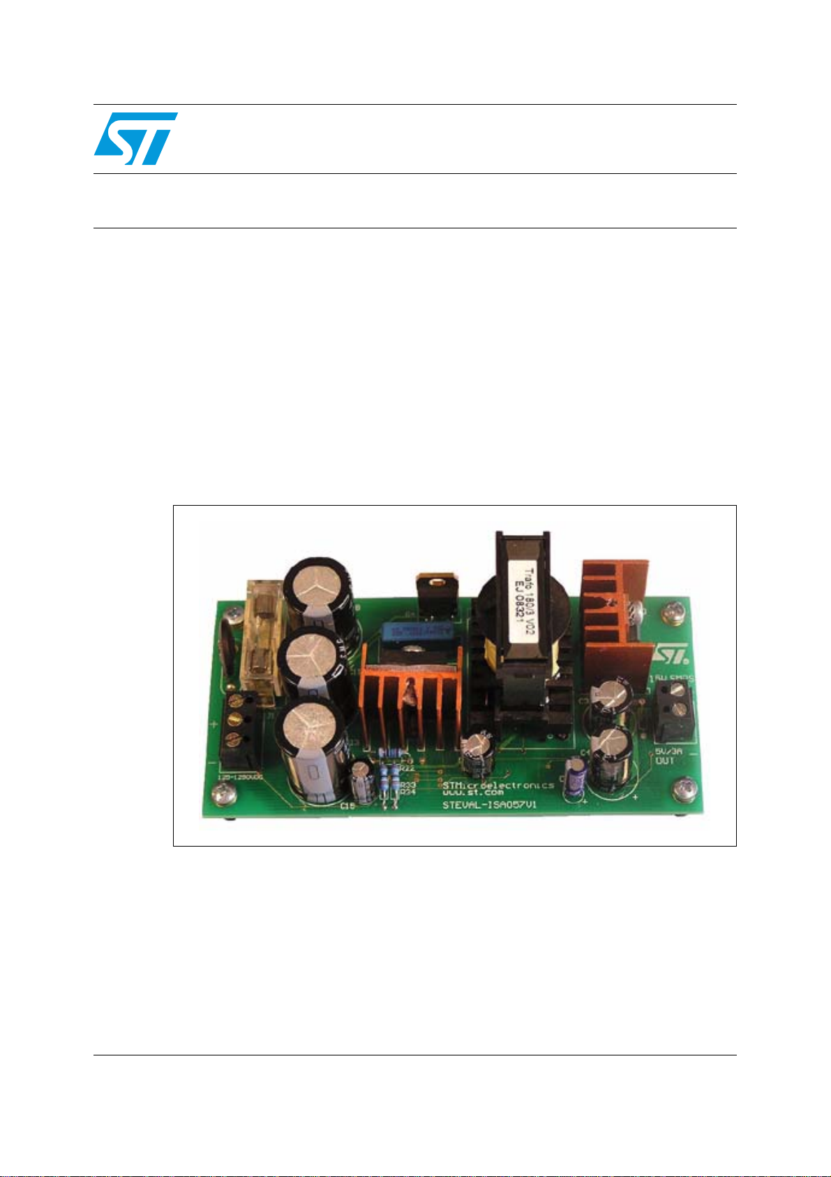
STEVAL-ISA057V1 (Figure 1).
Figure 1. STEV AL- ISA057V1
March 2009 Rev 1 1/37
www.st.com
Page 2

Contents AN2844
Contents
1 Introduction . . . . . . . . . . . . . . . . . . . . . . . . . . . . . . . . . . . . . . . . . . . . . . . . 1
2 Adapter features . . . . . . . . . . . . . . . . . . . . . . . . . . . . . . . . . . . . . . . . . . . . 5
2.1 Main characteristics . . . . . . . . . . . . . . . . . . . . . . . . . . . . . . . . . . . . . . . . . . 5
2.2 Circuit description . . . . . . . . . . . . . . . . . . . . . . . . . . . . . . . . . . . . . . . . . . . . 5
3 Waveforms and results . . . . . . . . . . . . . . . . . . . . . . . . . . . . . . . . . . . . . . 10
4 Electrical performances . . . . . . . . . . . . . . . . . . . . . . . . . . . . . . . . . . . . . 17
5 Functional check . . . . . . . . . . . . . . . . . . . . . . . . . . . . . . . . . . . . . . . . . . . 21
5.1 Startup behavior at full loads . . . . . . . . . . . . . . . . . . . . . . . . . . . . . . . . . . 21
5.2 Power-down . . . . . . . . . . . . . . . . . . . . . . . . . . . . . . . . . . . . . . . . . . . . . . . 22
5.3 Short-circuit tests . . . . . . . . . . . . . . . . . . . . . . . . . . . . . . . . . . . . . . . . . . . 22
6 Thermal measurements . . . . . . . . . . . . . . . . . . . . . . . . . . . . . . . . . . . . . 25
7 Bill of materials . . . . . . . . . . . . . . . . . . . . . . . . . . . . . . . . . . . . . . . . . . . . 26
8 PCB layout . . . . . . . . . . . . . . . . . . . . . . . . . . . . . . . . . . . . . . . . . . . . . . . . 28
9 Transformer specification . . . . . . . . . . . . . . . . . . . . . . . . . . . . . . . . . . . 30
9.1 Electrical characteristics . . . . . . . . . . . . . . . . . . . . . . . . . . . . . . . . . . . . . . 30
9.2 Mechanical aspects . . . . . . . . . . . . . . . . . . . . . . . . . . . . . . . . . . . . . . . . . 31
10 Ordering information . . . . . . . . . . . . . . . . . . . . . . . . . . . . . . . . . . . . . . . 33
11 Conclusion . . . . . . . . . . . . . . . . . . . . . . . . . . . . . . . . . . . . . . . . . . . . . . . . 34
12 References . . . . . . . . . . . . . . . . . . . . . . . . . . . . . . . . . . . . . . . . . . . . . . . . 35
13 Revision history . . . . . . . . . . . . . . . . . . . . . . . . . . . . . . . . . . . . . . . . . . . 36
2/37
Page 3

AN2844 List of tabl es
List of tables
Table 1. Line and load regulation . . . . . . . . . . . . . . . . . . . . . . . . . . . . . . . . . . . . . . . . . . . . . . . . . . . 17
Table 2. Efficiency at 125 VDC . . . . . . . . . . . . . . . . . . . . . . . . . . . . . . . . . . . . . . . . . . . . . . . . . . . . . 19
Table 3. Effic iency at 500 VDC. . . . . . . . . . . . . . . . . . . . . . . . . . . . . . . . . . . . . . . . . . . . . . . . . . . . . 19
Table 4. Efficiency at 1000 VDC. . . . . . . . . . . . . . . . . . . . . . . . . . . . . . . . . . . . . . . . . . . . . . . . . . . . 19
Table 5. Power consumpt ion in no-load conditions . . . . . . . . . . . . . . . . . . . . . . . . . . . . . . . . . . . . . 20
Table 6. Temperature of key componen ts at 125 VDC - full load
(3 A output current). . . . . . . . . . . . . . . . . . . . . . . . . . . . . . . . . . . . . . . . . . . . . . . . . . . . . . . 25
Table 7. Temperature of key componen ts at 1250 VDC - low load
(3 A output current). . . . . . . . . . . . . . . . . . . . . . . . . . . . . . . . . . . . . . . . . . . . . . . . . . . . . . . 25
Table 8. Bill of materials . . . . . . . . . . . . . . . . . . . . . . . . . . . . . . . . . . . . . . . . . . . . . . . . . . . . . . . . . . 26
Table 9. Winding characteristics. . . . . . . . . . . . . . . . . . . . . . . . . . . . . . . . . . . . . . . . . . . . . . . . . . . . 31
Table 10. Document revision history . . . . . . . . . . . . . . . . . . . . . . . . . . . . . . . . . . . . . . . . . . . . . . . . . 36
3/37
Page 4

List of figures AN2844
List of figures
Figure 1. STEVAL- ISA057V1 . . . . . . . . . . . . . . . . . . . . . . . . . . . . . . . . . . . . . . . . . . . . . . . . . . . . . . . 1
Figure 2. Electrical diagram . . . . . . . . . . . . . . . . . . . . . . . . . . . . . . . . . . . . . . . . . . . . . . . . . . . . . . . . . 6
Figure 3. ESBT - internal schematic and symbol. . . . . . . . . . . . . . . . . . . . . . . . . . . . . . . . . . . . . . . . . 7
Figure 4. V
Figure 5. V
Figure 6. V
Figure 7. V
Figure 8. 620 VDC and maximum output power in steady-state conditions . . . . . . . . . . . . . . . . . . . 12
Figure 9. 620 VDC and no output power (no load) in steady-state conditions. . . . . . . . . . . . . . . . . . 13
Figure 10. 620 VDC and maximum output power in steady-state conditions
Figure 11. 620 VDC and maximum output power in steady-state conditions
Figure 12. 1250 VDC and maximum output power in steady-state conditions . . . . . . . . . . . . . . . . . . 14
Figure 13. 1250 VDC and no output power (no load) in steady-state conditions. . . . . . . . . . . . . . . . . 15
Figure 14. 1250 VDC and maximum output power in steady-state conditions
Figure 15. 1250 VDC and maximum output power in steady-state conditions
Figure 16. Efficiency versus output power at V
Figure 17. Efficiency versus output power at V
Figure 18. Efficiency versus output power at V
Figure 19. Connector description. . . . . . . . . . . . . . . . . . . . . . . . . . . . . . . . . . . . . . . . . . . . . . . . . . . . . 21
Figure 20. Startup at 125 VDC. . . . . . . . . . . . . . . . . . . . . . . . . . . . . . . . . . . . . . . . . . . . . . . . . . . . . . . 21
Figure 21. Power-down at 125 VDC . . . . . . . . . . . . . . . . . . . . . . . . . . . . . . . . . . . . . . . . . . . . . . . . . . 22
Figure 22. Short-circuit test at V
Figure 23. Short-circuit test at V
Figure 24. Short-circuit test at V
Figure 25. Silk screen - top side . . . . . . . . . . . . . . . . . . . . . . . . . . . . . . . . . . . . . . . . . . . . . . . . . . . . . 28
Figure 26. Silk screen - bottom side . . . . . . . . . . . . . . . . . . . . . . . . . . . . . . . . . . . . . . . . . . . . . . . . . . 28
Figure 27. Copper tracks - top side . . . . . . . . . . . . . . . . . . . . . . . . . . . . . . . . . . . . . . . . . . . . . . . . . . . 29
Figure 28. Copper tracks - bottom side . . . . . . . . . . . . . . . . . . . . . . . . . . . . . . . . . . . . . . . . . . . . . . . . 29
Figure 29. Electrical diagram of the transformer . . . . . . . . . . . . . . . . . . . . . . . . . . . . . . . . . . . . . . . . . 30
Figure 30. Winding position . . . . . . . . . . . . . . . . . . . . . . . . . . . . . . . . . . . . . . . . . . . . . . . . . . . . . . . . . 31
Figure 31. Hole arrangement. . . . . . . . . . . . . . . . . . . . . . . . . . . . . . . . . . . . . . . . . . . . . . . . . . . . . . . . 32
= 125 VDC and maximum output power in steady-state conditions. . . . . . . . . . . . . . . 10
IN
= 125 VDC and no output power (no load) in steady-state conditions . . . . . . . . . . . . . 11
IN
= 125 VDC and maximum output power in steady-state conditions
IN
- switch-ON highlighted. . . . . . . . . . . . . . . . . . . . . . . . . . . . . . . . . . . . . . . . . . . . . . . . . . . . 11
= 125 VDC and maximum output power in steady-state conditions
IN
- switch-OFF highlighted. . . . . . . . . . . . . . . . . . . . . . . . . . . . . . . . . . . . . . . . . . . . . . . . . . . 12
- switch-ON highlighted. . . . . . . . . . . . . . . . . . . . . . . . . . . . . . . . . . . . . . . . . . . . . . . . . . . . 13
- switch-OFF highlighted. . . . . . . . . . . . . . . . . . . . . . . . . . . . . . . . . . . . . . . . . . . . . . . . . . . 14
- switch-ON highlighted. . . . . . . . . . . . . . . . . . . . . . . . . . . . . . . . . . . . . . . . . . . . . . . . . . . . 15
- switch-OFF highlighted. . . . . . . . . . . . . . . . . . . . . . . . . . . . . . . . . . . . . . . . . . . . . . . . . . . 16
= 125 VDC . . . . . . . . . . . . . . . . . . . . . . . . . . . . . . . 17
IN
= 500 VDC . . . . . . . . . . . . . . . . . . . . . . . . . . . . . . . 18
IN
= 1000 VDC . . . . . . . . . . . . . . . . . . . . . . . . . . . . . . 18
IN
= 125 VDC. . . . . . . . . . . . . . . . . . . . . . . . . . . . . . . . . . . . . . . . . . . 23
IN
= 620 VDC. . . . . . . . . . . . . . . . . . . . . . . . . . . . . . . . . . . . . . . . . . . 23
IN
= 1250 VDC. . . . . . . . . . . . . . . . . . . . . . . . . . . . . . . . . . . . . . . . . . 24
IN
4/37
Page 5

AN2844 Adapter features
2 Adapter features
2.1 Main characteristics
The following is a list of the specifications and main parameters of the demonstration board.
●
Minimum input voltage: 125 VDC
●
Maximum input voltage: 1250 VDC
●
Output voltage: 5 V - 3.0 A
●
Maximum output power: 15 W
●
Short-circuit protection based on auto-res tart feature
●
Minimum switching frequency limited to 30 kHz
●
Overall converter efficiency > 60%
●
Non-galvanic isolated solution used in most metering applications
●
PCB type and size:
– material used for PCB: FR-4
– double-sided layout
– thickness of copper: 35 µm
– total diameter of demonstration board: 58 x 120 mm.
2.2 Circuit description
This device is a flyback converter, a very popular and well-known topology in switch-mode
power supply applications where the required output power is in the range of
5 to 200 W. The popularity of this type of converter comes from the simplicity of its design,
the small number of components and its resulting low cost compared to other topologies in
the same output power range.
The converter is based on the L6565 PWM driver that operates in quasi-resonant mode,
meaning zero voltage or valley switching during the turn-OFF phase. Current mode control
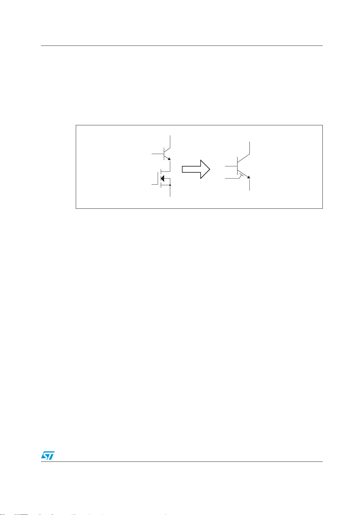
is the pri mary con tr o l method. An ESBT switch must be used for t hi s appl ication. The ESBT
is a cascade configuration of a high-voltage bipolar junction transistor (BJT) and a lowvoltage power MOSFET. STMicroelectronics™ optimizes the performance of both devices
and offers this kind of switch in one single package so as to simplify the application’s design,
reduce electromagnetic interference and price, and increase reliability and performance
(see Figure 3). The ESBT switch, compa r e d to a high-volta ge switch, offers a low ON-state
voltage drop like a BJT. The switch is very robust, easy to drive and has a relatively fast
switching speed similar to that of a MOSFET.
For more detailed information on the design of the discontinuous conduction-mode flyba ck
converter, refer to the application note AN1889 "ESBT STC03DE170HV in
3-phase auxiliary power supply".
5/37
Page 6
Adapter features AN2844
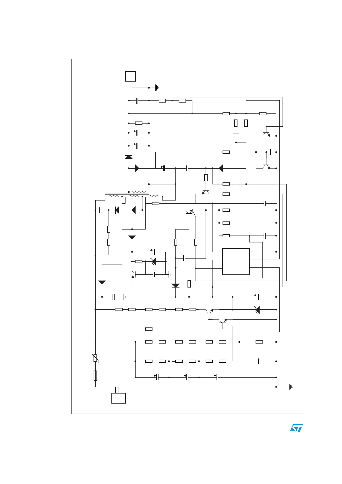
Figure 2. Electrical diagram
GND
+
1
2
5 V / 3 A
J2
OUT
connector
C5
100 nF
AM003536
T1 transf_ETD_29
C1
15 W SMPS 5 V / 3 A
Lp = 5.8 mH
Np / Ns = 70.2
1
Primary
2.2 nF / 2000 V
R3
R2
D1 BAV103
D3
STPS10L60
12
2
3
Primary
D2
STTH112D5STTH112
120 kΩ / 0.6 W
D4 STPS1150
120 kΩ / 0.6 W
Q1 2STF1360
C2
100 nF
C4
C3
R5
D6
Secondary
467
n.c.
BAV103
2.2 kΩ
R7
10
1000 µF
1000 µF
56 kΩ
R12 aux.
C7
D7
15 V
68 nF
C6
R16
C9
47 µF / 50 V
12 kΩ
2.2 µF
D8
12 kΩ
R21
C12
12 nF
Q3
BC847
Q2
STC03DE220HV
1
4
2
3
22 Ω
1.5 ΩR20
R26
C10
10 nF
R22
BAV103
910 Ω / 0.6 W
R27
GND
INV
FF
V
R42
10 kΩ
270 kΩ
Q7
BC847
47 nF
C19
Q6
BC847
C18
33 pF
C17
470 pF
6
1
3
C15
68 µF
/ 25 V
R38
10 kΩ
470 Ω
R39
R40
C14
100 pF
33 kΩ
R37
D9
BAV103
82 kΩ
R34
R36
R35
5
8
7
R33
R32
U1
ZCD
CC
V
OUT
910 Ω
10 kΩ
3.9 Ω
3.9 Ω
1 kΩ
L6565
2
COMP
CS
4
56 kΩR456 kΩ
R6
R10
R1 10 Ω
F1
Fuse 1 A
123
IN
J1
connector
R15
56 kΩ
R11
680 kΩ
R9
1.8
MΩ
R8
R13
200 kΩ
33 µFC8450 V
6/37
D10
Q4
STP03D200
56 kΩ
56 kΩ
R19
R25
1.8 MΩR14
1.8 MΩR18
200 kΩ
200 kΩ
R17
200 kΩ
R23
33 µF
450 V
C11
Q5
56 kΩ
1.8 MΩR24
R28
1.8 MΩR29
200 kΩ
C13
BC847
R30
33 µF
450 V
R31
1.8 MΩ
200 kΩ
18 V
R41
C16
22 kΩ
10 nF
Page 7
AN2844 Adapter features
The operational voltage of the converter ranges from 125 to 1250 VDC, which enables the
demonstration board to be used in various technologies, particular ly in metering
applications. The output voltage is 5 V and the maximum output power is 15 W.
The board is protected with a 1-A fuse in the primary area. A negative temperature
coefficient (NTC) resistor is inserted in series with the input line to protect the demonstration
board from inrush current. For voltage purposes on the input DC line, the main 450 V
filtering capacitors are connected in series.
Figure 3. ESBT - internal schematic and symbol
C
C
B
B
G
G
S
S
AM003535
A non-dissipative active startup circuit has been implemented to optimize the converter’s
efficiency. The alternative option of using a pure resistive startup circuit was rejected due to
unacceptable power losses. The active startup circuit has been design ed with Q4, Q5 and
related passive parts. The R4, R6, R11, R15, R19 and R25 resistors provide the supply
current to the PWM driver during the start-up phases and have been calculated from the
minimal input supply voltage of the converter and required supply current of the PWM
controller L6565, plus the related supply current required to charge the C15 filtering
capacitor within a reasonable time to maintain an acceptable startup time. The balance
resistors R8, R13, R17 and R23 are used to ensure the same voltage drop across each
input capacitor. R28 and R30 supply the current into the base of the Q4 high-voltage
Darlington transistor. When the rising voltage on the C15 capacitor reaches the start-up
threshold of the L6565 PWM controller, the voltage on the transformer's auxiliary winding
turns on the Q5 transistor, which in turn shorts the base of the Q4 transistor. This means
that the active startup is blocked. The main power dissipation under normal working
conditions of the startup circuit is due to the balance resistors. Refer to AN2454 "Universal
input voltage power supply for ESBT-based breaker and metering applications" for more
information on active startup issues.
The self-supply circuit that provides the supply energy to the controller has been built
around Q1, which acts as a linear voltage regulator. This voltage regulator offers a stable
output supply voltage, which guarantees the performance of the converter’s overall input
voltage range at very low or no loads. The voltage regulator is mandatory in such
applications with a wide input voltage range. The value of the auxiliary voltage is set with the
Zener diode D7 and is approximately 14.5 V. The primary side of the converter incorporates
the L6565 PWM controller that includes all the features required for building a complete
system working in QR mode with a minimal number of external components.
Information relating to the zero voltage switching comes from the transformer’s auxiliary
winding. The auxiliary winding is also used for the controller’s self-supply. To k eep a
relatively constant output power across the entire input voltage range, the line voltage is fed
through resistors R9, R14, R18, R24, R29 and R31 into the line voltage feed-forward pin
(V
) of the L6565.
FF
7/37
Page 8

Adapter features AN2844
This information is used to change the set point of the pulse-by-pulse current limitation. In
the standard application circuit with L6565 as U1, an OFF-time limitation circuit with a Q3
transistor has been added. This transistor limits the maximum switching frequency of the
converter to approximately 70 kHz. The input information coming from the OUT pin is fed
into Q3 with a delay. This feature provides some anticipated time dur ing the OFF time by
blocking the ZCD pin of the converter, and enables the reflected voltage on the auxiliary
winding to be sensed after that time. This means that the controller has skipped one or
several v alleys of the flyback voltage during the turn-OFF phases and has limited the
maximum switching frequency . The circuit’s time constant is set with capacitor C12 and
resistor R36. The limitations of the application’s frequency keep power losses on the
primary ESBT switch within reasonable values and contribute to the converter’s overall
stability. Refer to the L6565 datasheet for detailed information on the L6565 and function of
the circuit. All features, including the calculation of all setting components, are described in
STMicroelectronics’ application note AN1326 "L 6565 quasi-resonant controller". This
application note also describes the ZVS concept.
The output voltage is controlled by a non-galvanic isolated primary feedback loop with
resistor dividers R38 and R42, and frequency response compensation components R39,
R40 and C14. All formulas related to the calculation of the frequency response
compensation during first trials and testing in this type of application are described in
STMicroelectronics’ application note AN2495 "8 0 W very wide input voltage range 3-phase
SMPS design based on L6565 and ESBT STC04IE170HV".
In SMPS applications, where the load can vary, the current of the primary switch also
fluctuates. To minimize power losses on the ESBT switch, the base current should be
proportional to the collector current or at least constant with the initial current overpeak of
the switching pulse - this is called the modifying envelope. It is impor tant to avoid radical
over-saturation of the device at low loads and aim to optimize performance at full loads. To
achieve these driving requirements with a cost-effective solution, a simple driving circuit
providing a constant current into the base of the ESBT has been designed. This type of
solution is simple, cost-effective and minimizes power losses. The bias current for the base
of the ESBT is provided directly by the auxiliary power supply through the R22 resistor. For
a related base bias current, the value of this resistor is calculated according to the collector
current. According to the STC03DE220HV datasheet, for a maximum peak collector current
of 0.6 A, the gain and related base current should be 16 mA. During the storage time, when
the collector current for a c ertain period flows trough the B-C junction before this junction
recovers from conduction, the current flows into the C10 capacitor which stores some
energy and provides it again for the next switching cycle to create an initial base current
spike. Current that is not stored can also flow through D8 to the auxiliary supply area. Note
that during the storage time the collector current flows through the base and is stored in the
base capacitor C10, so that the quasi totality of energy is recovered. The R20 resistor limits
the inrush current floating from the C10 capacitor to the base of the Q2 transistor. In this
topology, the base current always has the same value and does not follow the variation of
the collector current, which appears while unloading the output. The constant base bias
current can caus e over-saturation of th e BJT struct u r e in the ESBT in low- or no-load
conditions. However, in a case like this, the driver guarantees the appropriate switching of
the ESBT th r ough the ZVS pin when the device is fully switched OFF and the carriers in the
BJT are fully recombined. This solution – which is very simple and cost-effective – implies
that the ESBT be driven with a constant current.
8/37
Page 9

AN2844 Adapter features
ESBTs with this type of configuration offer very good performance in terms of power losses,
and have a low cost compared to other available switches such as very high voltage power
MOSFETs. For further information on driving networks, refer to STMicroelectronics’
application note AN2454 "Universal input voltage power supply for ESBT-based breaker and
metering applications".
The main T1 transformer used is a layered-type transformer, which uses a standard ETD29
core with a bobbin. The ETD29 bobbin has been chosen because of its strong voltage
isolation capacities at such high input voltages. In terms of just power requirements, an even
smaller core area than the ETD29 could be used. A sandwich topology has been used for
the design of the winding, offering better coupling of windings compared to standard
topologies with only one primary winding.
This transformer has been designed according to STMicroelectronics’ released application
notes, with a flyback voltage of 250 V. The turn ratio between the primary and secondary
side has been calculated and is approximately 70. Refer to AN1326 "Quasi-resonant
controller" and AN2495 "80 W very wide input voltage range 3-phase SMPS design based
on L6565 and ESBT STC04IE170HV" for all necessary calculations.
As is common in flyback applications, the total voltage across the switch can reach very high
voltages. The calculation is done with the formula:
V
= V
OFF
where Vfl is the flyback voltage = (V
the primary side while Ns is the number of turns on the secondary side. V
inmax
+ Vfl + V
spike
+ VF diode) x Np/Ns. Np is the number of turns on
OUT
spike
is the
maximum overvoltage allowed by the clamping network and has been fixed to 200 V.
Allowing for som e m argin, a related switch STC03DE220HV with a breakdown voltage of
2200 V fills the requirements for these types of applicatio n.
A clamp network is used for leakage inductance demagnetization. In this particular case,
a C1 capacitor with related passive resistors R2, R3 and bl ocking diodes D2 and D5 used in
series because of voltage stresses, has been selected for this purpose.
The secondary side comprises a S chot tky barri er diode D3 as rectifier, and filtering
capacitors C3 and C4 featuring low serial resistance. The short-circuit protection features for
the converter have been designed with transistors Q7 and Q6 and related passive parts.
The Q7 transistor senses the output voltage through the resistor dividers R38 and R42. In
normal conditions, the Q7 transistor keeps the Q6 transistor turned off. During a short-circuit
condition where the output voltage is very low or e qual to zero, the Q7 transistor is closed.
Energy stored in the tank capacitor C9 can start to provide the supply current for Q6, which
starts to block the function of the converter through the L6565’s ZCD pin. This condition
continues until all the energy from the C9 capacitor has been discharged. The time cycle is
set with the R37 resistor and capacity of C9. Once all the energy in C9 has been
discharged, the converter star ts to work again. If the short connection on the output is still
present, the short-circuit protection repeats until the short circuit is removed.
9/37
Page 10
Waveforms and results AN2844
3 Waveforms and results
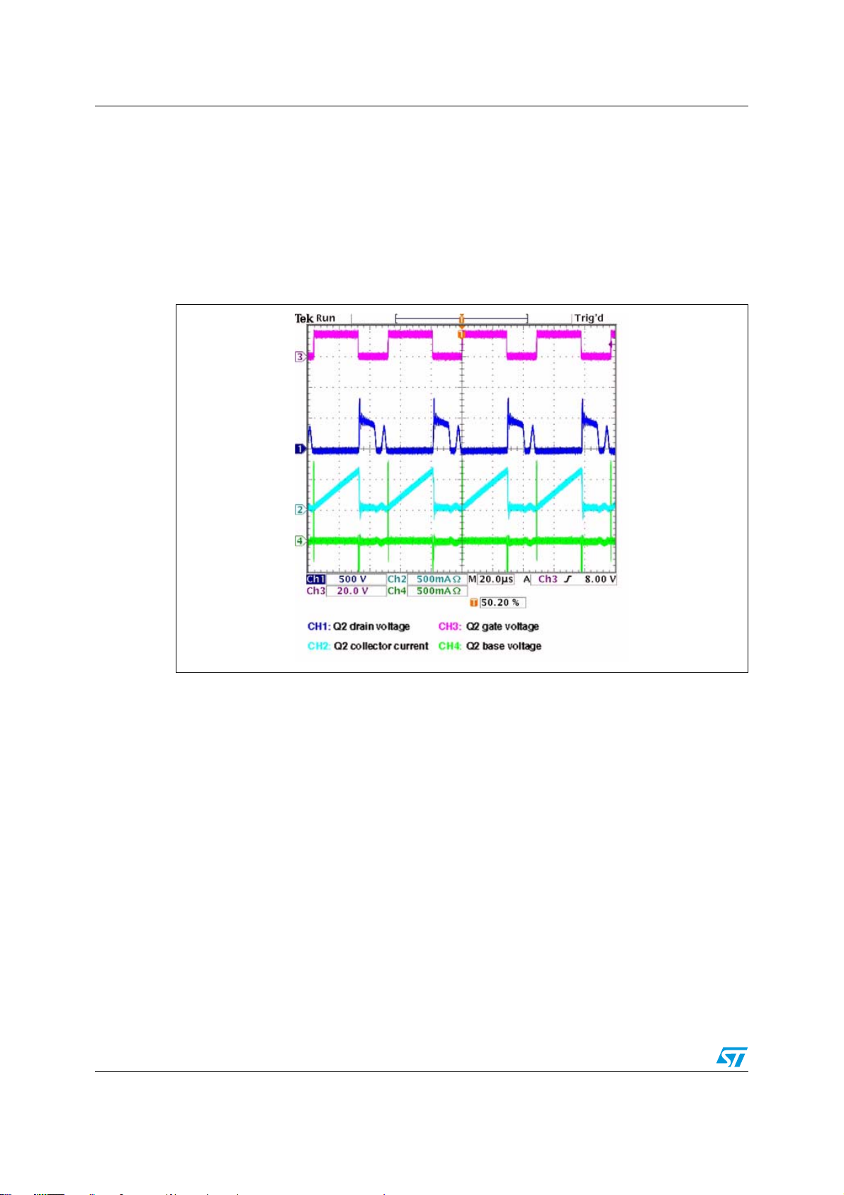
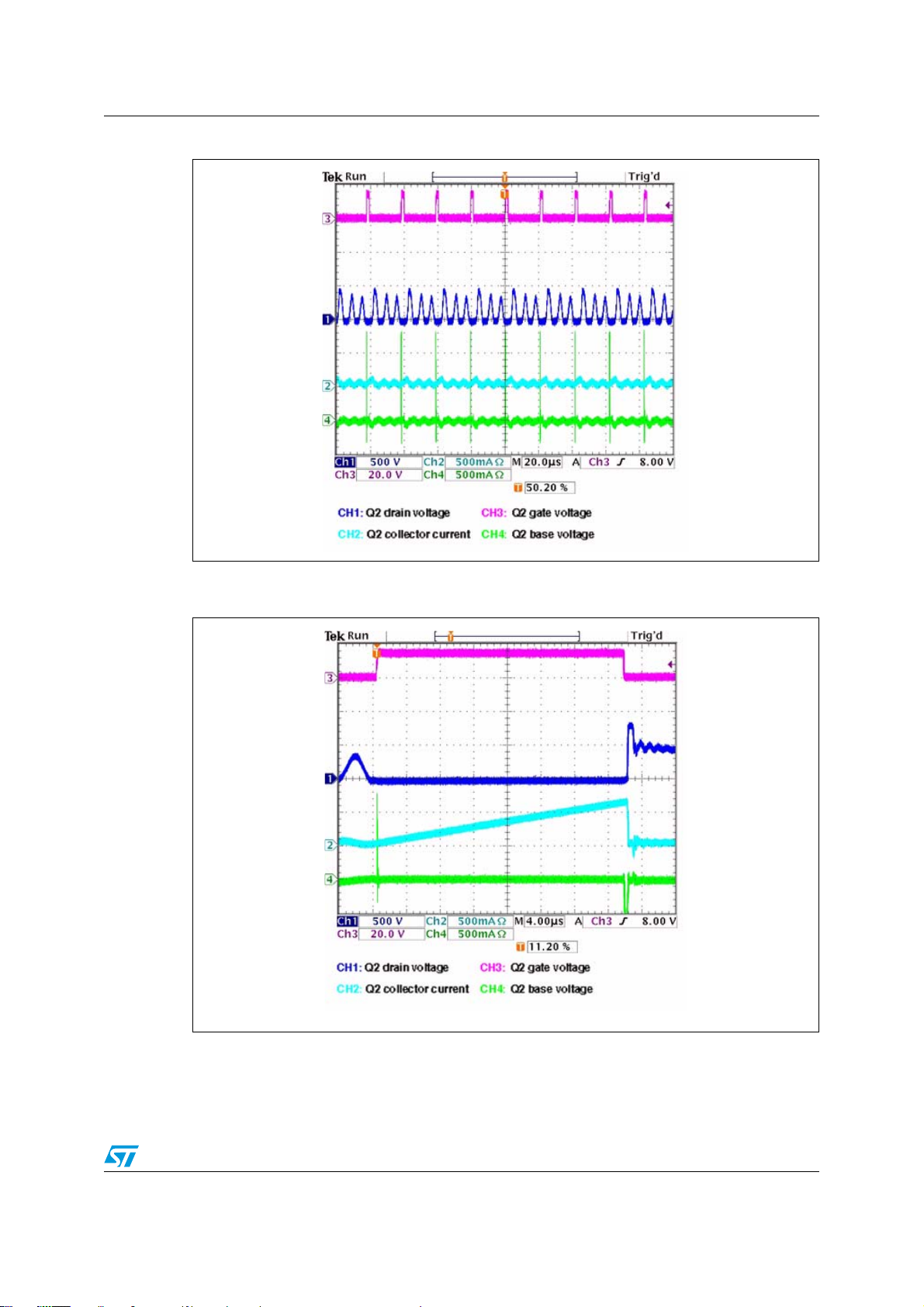
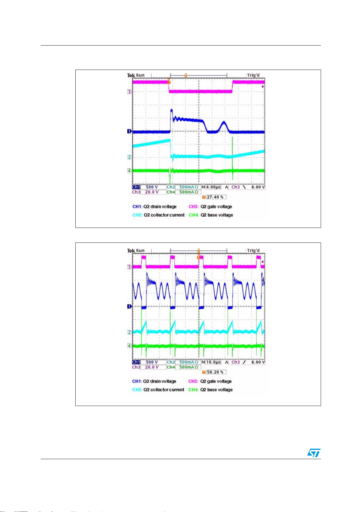
Figure 4 to Figure 15 show the main waveforms in steady-state conditions, and depict the
function of the converter with full loads or no loads and with var ious inpu t voltages. The
figures also show the turn-ON and turn-OFF behavior in various conditions. Of particular
interest is the behavior of the base current, where an initial high-peak pulse is needed to
minimize the effect of the dynamic saturation voltage.
Figure 4. V
= 125 VDC and maximum output power in steady-state conditions
IN
10/37
Page 11
AN2844 Waveforms and results
Figure 5. VIN = 125 VDC and no output power (no load) in steady-state conditions
Figure 6. V
= 125 VDC and maximum output power in steady-state conditions
IN
- swi tch-ON hig hli g hte d
11/37
Page 12
Waveforms and results AN2844
Figure 7. VIN = 125 VDC and maximum output power in steady-state conditions
- switch-OFF hig hl i ght e d
Figure 8. 620 VDC and maximum output power in steady-state conditions
12/37
Page 13

AN2844 Waveforms and results
Figure 9. 620 VDC and no output power (no load) in steady-state conditions
Figure 10. 620 VDC and maximum output power in steady-state conditions
- swi tch-ON hig hli g hte d
13/37
Page 14

Waveforms and results AN2844
Figure 11. 620 VDC and maximum output power in steady-state conditions
- switch-OFF highlighted
Figure 12. 1250 VDC and maximum output power in steady-state conditions
14/37
Page 15

AN2844 Waveforms and results
Figure 13. 1250 VDC and no output power (no load) in steady-state conditions
Figure 14. 1250 VDC and maximum output power in steady-state conditions
- switch-ON highlighted
15/37
Page 16

Waveforms and results AN2844
Figure 15. 1250 VDC and maximum output power in steady-state conditions
- switch-OFF highlighted
16/37
Page 17

AN2844 Electrical performances
4 Electrical performances
Table 1 shows the output loads for different input vo ltages. The maximum difference on the
output voltage is only about 50 mV.
Table 1. Line a n d lo a d regulation
Output load [A] Input voltage 125 VDC Input voltage 620 VDC Input voltage 1250 VDC
0 5.00 5.01 5.01
0.5 4.99 5.00 5.00
1 4.98 4.99 5.00
1.5 4.97 4.98 4.98
2 4.95 4.97 4.98
3 4.95 4.96 4.97
Figure 16, Figure 17 and Figure 18 show t he conv erter's efficiency depending on the output
load with various input voltage values.
Figure 16. Efficiency versus output power at V
Efficiency / output powe r
80
70
60
50
n (%)
40
30
20
10
0
0.00 5.00 10.00 15.00
P
OUT
= 125 VDC
IN
(W)
AM003544
17/37
Page 18

Electrical performances AN2844
Figure 17. Efficiency versus output power at VIN = 500 VDC
Efficiency / output powe r
80
70
60
50
n (%)
40
30
20
10
0
0 5 10 15
P
(W)
OUT
Figure 18. Efficiency versus output power at VIN = 1000 VDC
Efficiency / output powe r
80
70
60
50
n (%)
40
30
AM003545
20
10
0
0 5 10 15
18/37
P
OUT
(W)
AM003546
Page 19

AN2844 Electrical performances
Table 2. Efficiency at 125 VDC
Load [A] Pin [W ] P
0 0.27 0.00 0.00
0.2 1.85 0.97 52.43
0.5 3.70 2.45 66.22
0.8 5.62 3.91 69.57
1 6.94 4.88 70.32
1.2 8.27 5.84 70.62
1.5 10.31 7.27 70.51
2 13.94 9.64 69.15
2.5 17.80 11.96 67.19
3 21.93 14.28 65.12
:
Table 3. Efficiency at 500 VDC
Load [A] Pin [W ] P
00.4700.00
0.2 2.07 0.97 46.86
0.5 4.2 2.46 58.57
0.8 6.19 3.94 63.65
[W] Eff [%]
OUT
[W] Eff [%]
OUT
1 7.44 4.9 65.86
1.2 8.7 5.87 67.47
1.5 10.62 7.31 68.83
2 13.89 9.68 69.69
2.5 17.2 11.99 69.71
3 20.57 14.3 69.52
Table 4. Efficiency at 1000 VDC
Load [A] Pin [W ] P
01.500.00
0.2 3.31 0.97 29.31
0.5 5.68 2.46 43.31
0.8 7.99 3.94 49.31
1 9.4 4.91 52.23
1.2 10.49 5.88 56.05
1.5 12.45 7.33 58.88
2 16.37 9.69 59.19
2.5 19.66 12.03 61.19
[W] Eff [%]
OUT
3 22.94 14.33 62.47
19/37
Page 20

Electrical performances AN2844
Table 5 shows the device’s power consumption in no-load conditions.
Table 5. Power consu m pt i on i n no -load condit io ns
VIN = 125 VDC V
Pin [W] 0.27 0.47 1.50
= 500 VDC VIN = 1000 VDC
IN
This board has been designed to work in continuous cycles even with no loads. The reason
for this is an improved transfer response of the circuit, a lower output ripple and enhanced
stability of the converter.
The switching frequency of the ZVS control method used with the L6565 varies according to
the load and input voltage. This behavior has a positive impact on the switching losses
mainly in low-load conditions where the switching frequency rises dramatically to 60 kHz,
the maximum frequency that the application can tolerate.
20/37
Page 21

AN2844 Functional check
5 Functional check
Figure 19 shows the placement of the input and output connectors on the PCB.
Figure 19. Connector description
The following sections describe the main functional parameters of the board.
5.1 Startup behavior at full loads
Figure 20 shows the board’s startup behavior at full loads.
Figure 20. Star tup a t 1 25 VDC
21/37
Page 22

Functional check AN2844
5.2 Power-down
Figure 21 shows the reaction of the board when it is unplugged from the mains. The output
voltage as well as the auxiliary self-supply voltage have clear transitions with no glitches or
restart tri a ls.
Figure 21. Power-down at 125 VDC
5.3 Short-circuit tests
The following figures depict the board’s behavior when a short circuit occurs on the output
connector. Throughout the duration of a short-circuit condition, the output voltage is sensed
through logic circuits which contain Q6 and Q7 and the L6565 driver is shut down through
pin 5. Once all the energy from the C9 capacitor has been discharged, a logical stop reacts
on the output voltage and the board starts to operate normally. If the short-circuit condition
persists, the whole cycle repeats until the short-circuit condition stops. When a short-circuit
connection is removed, the converter starts to operate normally again.
22/37
Page 23

AN2844 Functional check
Figure 22. Short-circuit test at VIN = 125 VDC
Figure 23. Short-circuit test at V
= 620 VDC
IN
23/37
Page 24

Functional check AN2844
Figure 24. Short-circuit test at VIN = 1250 VDC
24/37
Page 25

AN2844 Thermal measuremen ts
6 Thermal measurements
A thermal analysis of the major components of the board is shown in Table 6 and Table 7. All
measurements were performed after one hour of operation.
: the ambient temperature for all measurements is 25 °C.
T
A
Table 6. Temperature of key components at 125 VDC - full load
(3 A output current)
Ref. Component description Temperature [°C]
R2 NTC 35
D2 Clamp resistors (R2; R3) 35
Q1 ESBT sw itch STC03DE220HV 37
U1 L6565 35
T1 Transformer - ferrite 44
T1 Transformer - windings 65
Q2 Output diode 80
C12/C13 Bulk capacitors 35
Table 7. Temperature of key components at 1250 VDC - low load
(3 A output current)
Ref. Component description Temper ature [°C]
R2 NTC 35
D2 Clamp resistors (R2; R3) 45
Q1 ESBT switch STC03DE220HV 75
U1 L6565 35
T1 T ransformer - ferrite 48
T1 Transformer - windings 55
Q2 Output diode 73
C12/C13 Bulk capacitors 35
25/37
Page 26

Bill of materials AN2844
7 Bill of materials
Table 8 presents the list of components used to build the demonstration board. The majority
of components used are available from STMicroelectronics. The main transformer is
supplied by EGSTON GmbH.
Table 8. Bill of materials
Index Quantity Reference
1 1 C1 2.2 nF / 700 VAC AXIALcap-RM 15 mm EPCOS
2 1 C2 100 nF Capacitor, SMD 0805 AVX
3 2 C3, C4 1000 µF / 10 V Elyt. capacitor, radial, RM 5 mm Rubycon
4 1 C5 100 nF Capacitor, SMD 0805 AVX
5 1 C6 68 nF Capacitor, SMD 0805 AVX
6 1 C7 47 µF / 50 V Capacitor, SMD 0805 Rubycon
7 3 C8, C11, C13 33 µF / 450 V Elyt capacitor, radial, RM 7.5 mm Rubycon
8 1 C9 2.2 µF / 10 V Elyt capacitor, radial, RM 2.5 mm Rubycon
9 1 C10 10 nF Capacitor, SMD 0805 AVX
10 1 C12 12 nF Capacitor, SMD 0805 AVX
11 1 C14 100 pF Capacitor, SMD 0805 AVX
12 1 C15 68 µF / 25 V Elyt capacitor , radial, RM 2.5 mm Rubycon
13 1 C16 10 nF Capacitor, SMD 0805 AVX
14 1 C17 470 pF Capacitor, SMD 0805 AVX
15 1 C18 33 pF Capacitor, SMD 0805 AVX
16 1 C19 47 nF Capacitor, SMD 0805 AVX
Value/generic
part number
Package/class Manufacturer
17 1 R1 10 Ω NTC resistor; RM 7.5 mm EPCOS
18 2 R2, R3 120 kΩ Resistor 0207; 0.6 W Vishay™
19 6
20 1 R5 Not connected Resistor 0207; 0.6 W Vishay
21 6
22 6
23 1 R10 680 kΩ Resistor, SMD 0805 Vishay
24 1 R7 2.2 kΩ Resistor, SMD 0805 Vishay
25 1 R12 56 kΩ Resistor, SMD 0805 Vishay
26 2 R16, R21 12 kΩ Resistor, SMD 0805 Vishay
27 1 R22 910 Ω Resistor 0207; 0.6 W Vishay
26/37
R4, R6, R11,
R15, R19, R25,
R8, R13, R17,
R23, R28, R30
R9, R14, R18,
R24, R29, R31
56 kΩ Resist or, SMD 1206 Vishay
200 kΩ Resistor, SMD 1206 Vishay
1.8 MΩ Resistor, SMD 1206 Vishay
Page 27

AN2844 Bill of materials
Table 8. Bill of materials (continued)
Index Quantity Reference
28 1 R26 22 Ω Resistor, SMD 0805 Vishay
29 1 R20 1.5 Ω Resistor, SMD 1206 Vishay
30 1 R27 82 kΩ Resistor, SMD 0805 Vishay
31 1 R41 22 kΩ Resistor, SMD 0805 Vishay
32 1 R32 1 kΩ Resistor, SMD 0805 Vishay
33 2 R33, R34 3.9 Ω Resi stor 0207; 0.6 W Vishay
34 1 R35 10 kΩ Resistor, SMD 0805 Vishay
35 1 R36 910 Ω Resistor, SMD 0805 Vishay
36 1 R37 33 kΩ Resistor, SMD 0805 Vishay
37 1 R39 470 Ω Resistor, SMD 0805 Vishay
38 1 R40 270 kΩ Resistor, SMD 0805 Vishay
39 2 R38, R42 10 kΩ Resistor, SMD 0805, 1% Vishay
40 4 D1, D6, D8, D9 BAV103 Diode, miniMELF Vishay
41 1 D4 STPS1150A Diode, DO-214AC STMicroelectronics
42 2 D2, D5 STTH112A HV diode, SMA STMicroelectronics
43 1 D3 STPS10L60D Power Schottky rectifier, TO-220AC STMicr oelectronics
44 1 D7 BZV55C15SMD Zener diode, SOD80, 15 V Vishay
Value/generic
part number
Package/class Manufacturer
45 1 D10 BZV55C18SMD Zener diode, SOD80, 18 V Vishay
46 1 Q1 2STF1360 NPN transistor, SOT-89 STMicroelectronics
47 1 Q2 STC03DE220HV ESBT, TO247-4L HV STMicroelectronics
48 4 Q3, Q5, Q6, Q7 BC847 NPN transistor, SOT-23 FAIRCHILD
49 1 Q4 STP03D200 NPN Darlington, TO-220 STMicroelectroni cs
50 1 U1 L6565D PWM smart driver, SO-8 STMicroelectronics
51 1 F1 Fuse 1 A Fuse with holder, 1 A, slow
52 1 J1 Connector ARK ARK
53 1 J2 ARK210/5 mm Connector ARK ARK
54 2 T1 EGSTON 39663 Transformer EGSTON ETD29 core EGSTON
55 2 Het1, Het2 V7142A Heatsink V7142A PADA Engineering
27/37
Page 28

PCB layout AN2844
8 PCB layout
The application uses a standard double-layer coppered PCB with a copper thickness of 35
µm. The PCB is made of FR-4.
The board’s diameters are:
●
length: 124.2 mm
●
width: 65.9 mm
●
thickness of PCB: 1.55 mm
Figure 25. Silk screen - top side
Figure 26. Silk screen - bottom side
28/37
Page 29

AN2844 PCB layout
Figure 27. Copper tracks - top side
Figure 28. Copper tracks - bottom side
29/37
Page 30

Transformer specification AN2844
9 Transformer specification
●
Application type: customer, home appliances
●
Winding type: layer
●
Coil former: vertical type - 14 pins
●
Material of coil former: GFR thermostatic plastic UL 94 V-0
●
Maximum temperature increase: 45° C
●
Maximum operating ambient temperature: 60° C
●
Mains insulation: according to EN60950
9.1 Electrical characteristics
●
Converter topology: flyback working in boundary mode
●
Minimum switching frequency: > 32 kHz
●
Lp = 5.8 mH
●
Np/Ns = 70.2
●
Reflected flyback voltage: 400 VDC
●
Core type: ETD29 - EPCOS
●
Core material: N87 from EPCOS or similar
●
Air gap: 0.60 mm
The design of the related power transformer has been fur ther optimized by EGSTON
System Electronics Eggenburg GmbH, manufacturer of the transformer. The ordering type
is 39663.
Figure 29. Electrical diagram of the transformer
1
2
3
4
6
7
1/2 A
PRIMARY
1/2 B
PRIMARY
AUXILIARY
12
SECONDAR Y 3T
10
AM003547
90 T
90 T
12 T
30/37
Page 31

AN2844 Trans former sp eci fication
For enhanced magnetic coupling, a sandwich topology has been used for the windings. The
secondary winding is placed beside the split of the primary winding. The primary winding
parts have half the total number of turns and are connected in series. The order of the
windings, starting from the winding nearest the core, is: PRIMARY - A , SECONDARY,
PRIMARY - B, an d t hen t he top AUXILIARY winding for the SMPS’ self-supply.
Table 9. Winding characteristics
Pins Winding Number of turns Wire type
1-2 PRIMARY - A 90 1 x AVG34
10-12 SECONDARY 3 3 x AVG24
3-4 PRIMARY - B 90 1 x AVG34
6-7
Figure 30. Winding position
3 mm 3 mm
Coil former Insulation tape
9.2 Mechanical aspects
●
Maximum height from PCB: 40 mm
●
Occupied area on PCB: 35 mm x 25 mm
●
Coil former: 14 pins
●
Diameter of pins: 1.3 mm + 0.1 mm
●
Raster of pins: 5 mm
Figure 31 shows the mechanical arrangement of the transformer. The figure should be
viewed from a mounting angle.
AUXILIARY
AUXILIARY
PRIMARY - B
SECONDAR Y
PRIMARY - A
12 1 x AVG32
AM003548
31/37
Page 32

Transformer specification AN2844
Figure 31. Hole arrangement
20
Mounting holes: 1,5
1
14
78
Top view
6 x 5.08
AM003549
32/37
Page 33

AN2844 Ordering information
10 Ordering information
The application board is orderable online at
http://www.st.com/stonline/domains/buy/buy_dev.htm with the order code
STEVAL-ISA057V1. The deliverabl e con tains the assembled application board, related
documentation, PCB manufacturing data such as gerber and assembly files (pick and place)
as well as component documentation.
33/37
Page 34

Conclusion AN2844
11 Conclusion
This document describes the flyback converter based on the quasi-resonant principle with
an ESBT switch driven by a constant current. SMPS is specifically designed for metering
applications where wide input voltage ranges are required. The use of an ESBT switch as
the main switch has the advantage of simplifying the circuit’s design and providing a costeffective solution.
34/37
Page 35

AN2844 References
12 References
1. STMicroelectronics L6565 device datasheet.
2. STMicroelectronics STC03DE220HV device datasheet.
3. STMicroelectronics applica tion note AN1326: L6565 quasi-resonant controller.
4. STMicroelectronics applica tion note AN1889: STC03DE170H V in 3-phase auxiliar y
power supply.
5. STMicroelectronics applica tion note AN2495: 80 W Very wide input voltage range
3-phase SMPS designed based on L6565 and ESBT STC04IE170HV.
6. STMicroelectronics applica tion note AN2454: Universal input voltage power supply for
ESBT-based breaker and metering applications.
35/37
Page 36

Revision history AN2844
13 Revision history
Table 10. Document revision history
Date Revision Changes
13-Mar-2009 1 Initial rel ease.
36/37
Page 37

AN2844
y
y
Please Read Caref u ll y:
Information in this document is provided solely in connection with ST products. STMicroelectronics NV and its subsidiaries (“ST”) reserve the
right to make changes, corrections, modifications or improvements, to this document, and the products and services described herein at an
time, with out notice.
All ST products are sold pursuant to ST’s terms and conditions of sale.
Purchase rs are solely responsible for the choi ce, selection and use of the ST products and services d escribed herein, and ST assumes no
liability whatsoever relating to the choice, selection or use of the ST products and services described herein.
No license, express or implied, by estoppel or otherwise, to any intellectual property rights is granted under this document. If any part of this
document refers to any third par ty products or services i t s hall not be d eem ed a licen se grant by ST f or the use of such third party products
or services , or any intel lec tual pro per ty cont aine d ther ein or consi dere d as a warra nty c overi ng th e use in any mann er w hats oever of such
third party products or s ervices or any i ntellectual property c ont ai ned therein.
UNLESS OTHERWISE SET FORTH IN ST’S TERMS AND CONDITIONS OF SALE ST DISCLAIMS ANY EXPRESS OR IMPLIED
WARRANTY WITH RESPECT TO THE USE AND/OR SALE OF ST PRODUCTS INCLUDING WITHOUT LIMITATION IMPLIED
WARRANTIES OF MERCHANTABILITY, FITNESS FOR A PARTICULAR PURPOSE (AND THEIR EQUIVALENTS UNDER THE LAWS
OF ANY JURISDICTION), OR INFRINGEMENT OF ANY PATENT, COPYRIGHT OR OTHER INTELLECTUA L PROPERTY RIGHT.
UNLESS EXPRESSLY APPROVED IN WRITING BY AN AUTHORIZED ST REPRESENTATIVE, ST PRODUCTS ARE NOT
RECOMM ENDED , AUTHO RIZED OR WARRANT ED FOR USE IN M ILITA RY, AIR CR AFT, SPA CE, LIF E SAVIN G, OR LIF E SUSTAI NING
APPLICATIONS, NOR IN PRODUCTS OR SYSTEMS WHERE FAILURE OR MALFUNCTION MAY RESULT IN PERSONAL INJURY,
DEATH, OR SEVERE PROPERTY OR ENVIRONMENTAL DAMA GE. ST PRODUCTS WHICH ARE NOT S PECI F IED AS "AU TO MOTI VE
GRADE" MAY ONLY BE USED IN AUTOMOTIVE APPLICATIONS AT USER’S OWN RISK.
Resale of ST products with provisions different from the statements and/or technical features set forth in this document shall immediately void
any warran ty gr anted by ST fo r the ST produc t or se rvice d es cribed he rein and shall not c reat e or ex tend in a ny mann er wha tsoe ver, an
liability of ST.
ST and the ST logo are trademarks or regis t ered trademarks of ST in vari ous countri es.
Information in this docum ent supersedes and replaces all information pr ev i ously suppli ed.
The ST logo is a registered trademark of STMicroelectronics. All other names are the property of their respective owners.
© 2009 STM icroelectro n ics - All rights reserved
STMicroelectron ics group of com panies
Austra l i a - Belgium - Brazil - Canada - China - Czech Republic - F i nl and - France - Germany - Hong Kong - India - Israel - Ital y - Japan -
Malaysi a - M al ta - Morocco - Singapore - Spain - Sweden - Switze rl and - Unite d Kingdom - Unit ed States of America
www.st.com
37/37
 Loading...