

Page 1

LED dimming implemented on STM32™ microcontroller
1 Introduction
This application note deals with the general principles of LED dimming. This note also
focuses on the use of pulse width modulation (PWM) for digital dimming. Its implementation
on the STM32
described in detail and the most common design approaches are compared.
The conclusion helps developers choose the best approach for their LED dimming
application.
™
microcontroller in combination with the STP24DP05 LED driver is
AN2841
Application note
November 2008 Rev 1 1/31
www.st.com
Page 2

Contents AN2841
Contents
1 Introduction . . . . . . . . . . . . . . . . . . . . . . . . . . . . . . . . . . . . . . . . . . . . . . . . 1
2 Description of LED dimming . . . . . . . . . . . . . . . . . . . . . . . . . . . . . . . . . . 5
2.1 Driving multiple LED applications . . . . . . . . . . . . . . . . . . . . . . . . . . . . . . . . 6
2.2 Multi-channel dimming using serial-parallel conversion . . . . . . . . . . . . . . . 6
2.3 Specific dimming application using an STP24DP05 . . . . . . . . . . . . . . . . . 8
3 Dimming application using an STM32 microcontroller . . . . . . . . . . . . . 9
3.1 Data transfers and timing . . . . . . . . . . . . . . . . . . . . . . . . . . . . . . . . . . . . . . 9
3.1.1 Dynamic data transfer . . . . . . . . . . . . . . . . . . . . . . . . . . . . . . . . . . . . . . . 9
3.1.2 Static data transfer using lookup tables . . . . . . . . . . . . . . . . . . . . . . . . . 12
3.1.3 Single interrupt . . . . . . . . . . . . . . . . . . . . . . . . . . . . . . . . . . . . . . . . . . . . 13
3.1.4 Single interrupt with DMA . . . . . . . . . . . . . . . . . . . . . . . . . . . . . . . . . . . 16
3.1.5 Interrupt + DMA + interrupt . . . . . . . . . . . . . . . . . . . . . . . . . . . . . . . . . . 17
3.2 Data preparation: redundant and non redundant use of memory . . . . . . 19
3.2.1 Full lookup table (redundant) . . . . . . . . . . . . . . . . . . . . . . . . . . . . . . . . . 19
3.2.2 Reduced lookup table (non redundant) . . . . . . . . . . . . . . . . . . . . . . . . . 20
3.3 Timing: set up of the main dimming timer . . . . . . . . . . . . . . . . . . . . . . . . 22
3.3.1 The main system timer, SysTick setting . . . . . . . . . . . . . . . . . . . . . . . . 22
4 Achieved values . . . . . . . . . . . . . . . . . . . . . . . . . . . . . . . . . . . . . . . . . . . 25
4.1 Dimming approach comparison and conclusion . . . . . . . . . . . . . . . . . . . 29
4.1.1 Comparison between interrupt and interrupt + DMA approaches . . . . . 29
4.1.2 Comparison between dynamic preparation, static, and reduced static
lookup table . . . . . . . . . . . . . . . . . . . . . . . . . . . . . . . . . . . . . . . . . . . . . . 29
5 References documents . . . . . . . . . . . . . . . . . . . . . . . . . . . . . . . . . . . . . . 30
6 Revision history . . . . . . . . . . . . . . . . . . . . . . . . . . . . . . . . . . . . . . . . . . . 30
2/31
Page 3

AN2841 List of tables
List of tables
Table 1. LEDmap - requested LED brightness configuration . . . . . . . . . . . . . . . . . . . . . . . . . . . . . . 19
Table 2. Full lookup table . . . . . . . . . . . . . . . . . . . . . . . . . . . . . . . . . . . . . . . . . . . . . . . . . . . . . . . . . 20
Table 3. LEDmap - requested LED brightness configuration . . . . . . . . . . . . . . . . . . . . . . . . . . . . . . 21
Table 4. LEDmap - reordered requested LED brightness configuration. . . . . . . . . . . . . . . . . . . . . . 22
Table 5. Reduced lookup table . . . . . . . . . . . . . . . . . . . . . . . . . . . . . . . . . . . . . . . . . . . . . . . . . . . . . 22
Table 6. TotalTime necessary for requested dimming parameters. . . . . . . . . . . . . . . . . . . . . . . . . . 23
Table 7. Maximum refresh rate . . . . . . . . . . . . . . . . . . . . . . . . . . . . . . . . . . . . . . . . . . . . . . . . . . . . . 23
Table 8. SysTick-reload-time for 100 Hz . . . . . . . . . . . . . . . . . . . . . . . . . . . . . . . . . . . . . . . . . . . . . 23
Table 9. Example of values used in Equations 3 and 4 . . . . . . . . . . . . . . . . . . . . . . . . . . . . . . . . . . 24
Table 10. Lookup table size (full and reduced). . . . . . . . . . . . . . . . . . . . . . . . . . . . . . . . . . . . . . . . . . 25
Table 11. Refresh frequencies . . . . . . . . . . . . . . . . . . . . . . . . . . . . . . . . . . . . . . . . . . . . . . . . . . . . . . 26
Table 12. Refresh frequencies for better optimized code (8 and 12-bit PWM) . . . . . . . . . . . . . . . . . . 28
Table 13. Refresh frequencies for better optimized code (10 and 11-bit PWM) . . . . . . . . . . . . . . . . . 28
Table 14. Document revision history . . . . . . . . . . . . . . . . . . . . . . . . . . . . . . . . . . . . . . . . . . . . . . . . . 30
3/31
Page 4

List of figures AN2841
List of figures
Figure 1. PWM signal with 16 steps of possible voltage values . . . . . . . . . . . . . . . . . . . . . . . . . . . . . 5
Figure 2. PWM serial-parallel conversion for multiple LED applications . . . . . . . . . . . . . . . . . . . . . . . 7
Figure 3. Example of a specific lighting setting . . . . . . . . . . . . . . . . . . . . . . . . . . . . . . . . . . . . . . . . . . 7
Figure 4. Simplified setup of an application using an STP24DP05 . . . . . . . . . . . . . . . . . . . . . . . . . . . 8
Figure 5. STM32 evaluation board setup . . . . . . . . . . . . . . . . . . . . . . . . . . . . . . . . . . . . . . . . . . . . . . 9
Figure 6. STM32 evaluation board block diagram . . . . . . . . . . . . . . . . . . . . . . . . . . . . . . . . . . . . . . . 9
Figure 7. Computation of LEDdriverDATAbuffer variable . . . . . . . . . . . . . . . . . . . . . . . . . . . . . . 10
Figure 8. Conversion of LEDmap array to LEDdriverDATAbuffer . . . . . . . . . . . . . . . . . . . . . . . . 11
Figure 9. Dynamic data preparation - time consumption - block diagram . . . . . . . . . . . . . . . . . . . . . 12
Figure 10. Dynamic data preparation - time consumption - real signals . . . . . . . . . . . . . . . . . . . . . . . 12
Figure 11. Static lookup table time consumption with 166 kHz - 333 kHz LE signal . . . . . . . . . . . . . . 13
Figure 12. Timing diagram: Single interrupt method . . . . . . . . . . . . . . . . . . . . . . . . . . . . . . . . . . . . . . 14
Figure 13. Real timing signals for single interrupt method . . . . . . . . . . . . . . . . . . . . . . . . . . . . . . . . . 14
Figure 14. Timing diagram: Single interrupt with DMA . . . . . . . . . . . . . . . . . . . . . . . . . . . . . . . . . . . . 16
Figure 15. Timer interrupt + DMA transfer + DMA interrupt. . . . . . . . . . . . . . . . . . . . . . . . . . . . . . . . . 17
Figure 16. Real signals: timer interrupt + DMA transfer + DMA interrupt model . . . . . . . . . . . . . . . . . 18
4/31
Page 5
AN2841 Description of LED dimming
2 Description of LED dimming
There are two categories of LED dimming:
●
Analog: Uses a linear device to set the current flow through the LED.
Advantages: Absence of digital noise; a simple implementation.
Limitations: Color shift, low dynamics.
●
Digital: Uses a switch to set nominal or zero current flow through the LED.
Advantages: Accurate and fast color control.
Limitations: The presence of digital noise and necessity to use a frequency high
enough to prevent flickering; a complex implementation.
This document focuses on digital dimming and the use of PWM (pulse width modulation) in
common applications.
When using PWM for lighting applications, the following rules must be kept in mind:
●
For the LED light to be seen as non-flickering by the human eye, in most cases the
PWM frequency must be higher than 100 Hz.
●
The LED light brightness depends on the PWM duty cycle. The brightness depends on
the resolution of the PWM duty cycle.
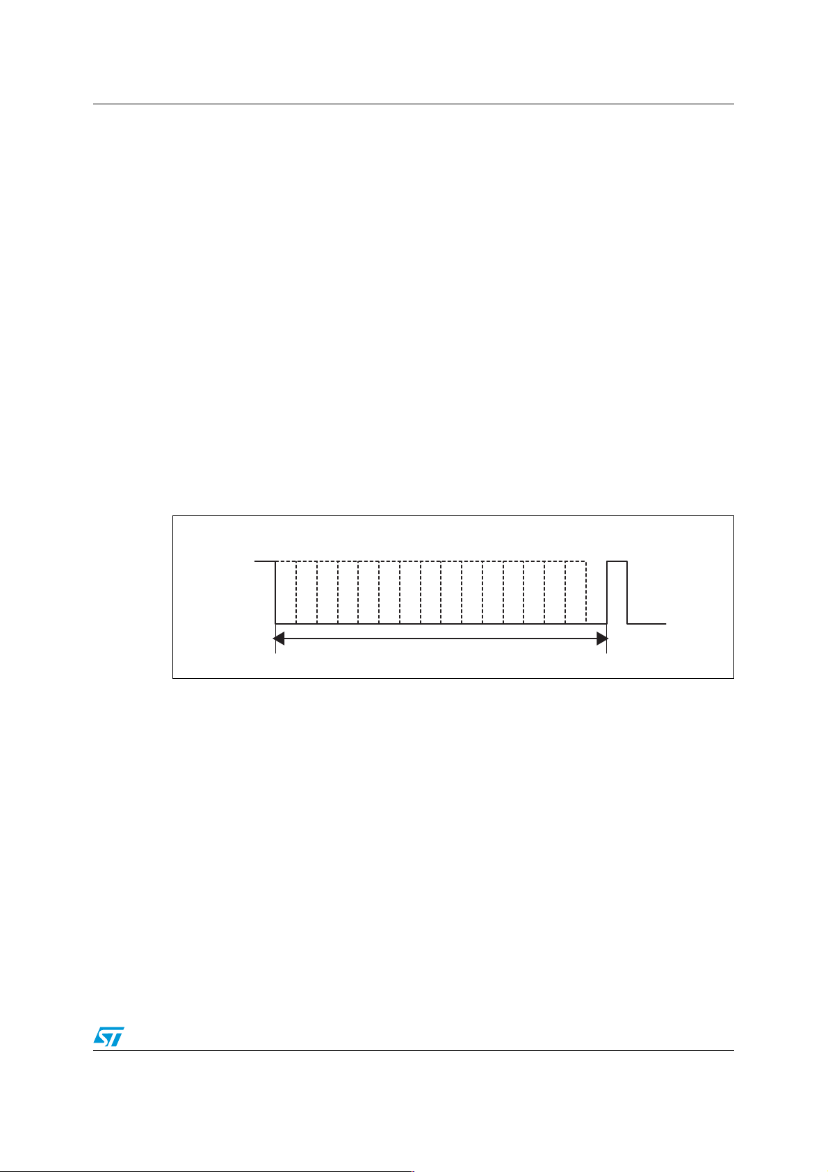
Figure 1. PWM signal with 16 steps of possible voltage values
Step: 0 1 2 3 4 5 6 7 8 9 10 11 12 13 14 15
T
PWM
0 1 ...
AM00341
Using a 4-bit PWM resolution, there can be 16 different light intensity (energy) values.
Concerning color applications, 16 million (256 × 256 × 256) colors can be reached using
tricolor LEDs with an 8-bit dimming resolution for each single color LED.
5/31
Page 6

Description of LED dimming AN2841
2.1 Driving multiple LED applications
Displays, indicators and panels increasingly use more and more LEDs. There are three
approaches for driving higher numbers of LEDs:
1. Dedicated pin
Each LED is driven by dedicated system (microcontroller, FPGA) pin.
Advantages: Simple implementation of dimming algorithm. No conversion.
Disadvantages: Unusable for high LED counts. Consumes pins of microcontroller.
2. Serial-parallel conversion
Multiple LEDs are driven by a single system pin.
Advantages: Reduced number of system pins required. High LED count systems can
be developed.
Disadvantages: Additional components and external buffers are needed. The data rate
on a single pin must be n times greater than that for the single LED out of n, where n is
the number of LEDs.
3. Matrix
LEDs are arranged in a square matrix and driven by a complex and sophisticated
algorithm that combines serial-parallel conversion with additional decomposition of the
serial data stream into the rows and columns by another active component.
This document focuses on serial-parallel conversion applications.
2.2 Multi-channel dimming using serial-parallel conversion
The serial-parallel conversion approach is in fact a parallel-serial-parallel conversion since
the data is stored in the system memory in parallel format and then is converted to serial
format before its transfer over the serial interface. The serial stream is then reconverted to
parallel format by the LED driver used to drive each LED. The serial data transfer speed
must be n times faster than driving a single LED, where n is the number of parallel driver
outputs.
Buffers (LED drivers) used for serial-parallel conversion come generally with the four most
important signals:
■
SDI: Serial data in
■
SDO: Serial data out
■
CLK: Clock signal used for loading data in the driver buffer via the SDI (input) and
sending data from the buffer via the SDO (output). It also shifts all data actually
present (previously loaded) in the driver.
■
LE: Copies (latch enable) the actual values loaded in the driver into its output cells.
The output cells drive parallel outputs.
The standard serial peripheral interface (SPI) contains SDO, SDI and CLK signals.
It is necessary to latch (LE signal pulse) internal driver data once per n CLK cycles, where
n is the total LED count. This latching rule ensures the correct mapping of the serialized
PWM data coming on SDI to the corresponding parallel output. Refer to Figure 2, Figure 3
and Figure 4.
6/31
Page 7
AN2841 Description of LED dimming
Figure 2. PWM serial-parallel conversion for multiple LED applications
Figure 3. Example of a specific lighting setting
T
PWM
SERIAL DATA
T
SEND_DATA
PARALLEL DATA
1101 0101 0001 0000
1111
LEVELS
1111 or new
data
t
Output 1 - ( L E D 1 )
Output 2 - ( L E D 2 )
Output 3 - ( L E D 3 )
Output 4 - ( L E D 4 )
4% duty cycle
14% duty cycle
3% duty cycle
99% duty cycle
t
t
t
t
AM00343
The following equation is used to determine how many LEDs can used in an application with
specific maximum SPI speed and PWM resolution requirements:
Equation 1
f
N
SPI
=
n
f
2
PWM
where;
N is the maximum number of LEDs
f
is the SPI communication speed
SPI
n is the PWM resolution
f
is the dimming frequency
PWM
7/31
Page 8

Description of LED dimming AN2841
The outcome of Equation 1 is valid only for the best-case scenario when the data are sent
to the LED driver without any delay between blocks of data. This example, of course, is not
a real one. The values for a real application can only get close to the value determined
above.
2.3 Specific dimming application using an STP24DP05
Figure 4 illustrates a simple dimming application using an STP24DP05 24-bit constant
current LED sink driver with output error detection.
Figure 4. Simplified setup of an application using an STP24DP05
5 V
3.3 V
LED block
Temperature
sensor
RGB LED configuration
Driving
system
R1...8 G1...8 B1...8
SPI
OE-R/G/B
STP24DP05
STP24DP05
SPI
LE
More drivers in cascade…
AM00344
8/31
Page 9
AN2841 Dimming application using an STM32 microcontroller
3 Dimming application using an STM32 microcontroller
This section describes a dimming application that uses an STM32 microcontroller (MCU).
All the computations, results and tests were performed on an evaluation board (reference:
STEVAL-ILL015V1) containing an STM32 MCU running at a clock frequency of 48 MHz.
For more information about the use of this evaluation board and dimming applications,
please refer to user manuals UM0588 and UM0574 listed in Section 5: References
documents.
Figure 5 and Figure 6 provide a brief overview of the STM32 evaluation board.
Figure 5. STM32 evaluation board setup
Figure 6. STM32 evaluation board block diagram
USB SPI
ESD for USB
USBUF01P6
Power supply
ST1S10
STM32
3.1 Data transfers and timing
This section describes the two approaches used to transfer data (dynamic and static) as
well as timing considerations.
3.1.1 Dynamic data transfer
When using a dynamic data approach, all data is computed just before being transfered to
the LED drivers.
LED driver
STP24DP05
SPI
LED driver
STP24DP05
SPI
AM00345
9/31
Page 10
Dimming application using an STM32 microcontroller AN2841
The LED brightness value is defined by the user in the LEDmap array. The LEDmap is an
array of 8-bit numbers (when using an 8-bit dimming resolution). Each value is dedicated
to one single LED (Figure 7).
The dimming algorithm converts the LEDmap array into a serial stream. The serial stream
in combination with the LE signal generates requested PWM outputs on the LED drivers
as shown in Figure 8.
Figure 7. Computation of LEDdriverDATAbuffer variable
Begin
depth = 0
DATAchar = 0
Detail in Figure 8:
LEDmap LEDdriverDATAbuffer
DATAchar++
–
–
DATAchar>3
+
depth++
depth>255
0 .. 255 for 8-bit PWM resolution
0 .. LEDcount / 8
SPI
Driver
LED
+
10/31
AM00346
Page 11

AN2841 Dimming application using an STM32 microcontroller
Figure 8. Conversion of LEDmap array to LEDdriverDATAbuffer
for one time stamp depth = 50
LEDmap = {20, 60, 75, 22, 100, 255, 0, 5}
LEDmap[0] > depth = 0
for outputBIT from 0 to 7
LEDmap[1] > depth = 1
LEDmap[2] > depth = 1
LEDmap[3] > depth = 0
LEDdriverDATAbuffer[0]
LEDmap[4] > depth = 1
LEDmap[6] > depth = 1
LEDmap[7] > depth = 0
LEDmap[8] > depth = 0
SPI
Example using a 4×8 LED matrix with an 8-bit PWM resolution
while(1)
for(depth = 1; depth<=0xff; depth++){
for(DATAchar = 0; DATAchar < 4; DATAchar++){
for(outputBIT = 0; outputBIT < 8; outputBIT++){
LEDdriverDATAbuffer[DATAchar] <<= 1;
if(LEDmap[(DATAchar*8) + outputBIT] > depth)
LEDdriverDATAbuffer[DATAchar] |= 0x0001;
else
LEDdriverDATAbuffer[DATAchar] &= 0xFFFE;
}
SPI_SendData(SPI1, LEDdriverDATAbuffer[DATAchar]);
}
LE_LOW();
LE_HIGH();
LE_LOW();
}
LED driver
AM00347
Even though the dynamic data preparation consumes a minimum of system memory, it
takes a lot of computational time. This approach is only recommended for low LED count
applications. A dynamic data preparation approach can reach 100 Hz for 32 LEDs (with
maximum code optimization in C compiler on the STM32 evaluation board).
11/31
Page 12

Dimming application using an STM32 microcontroller AN2841
Figure 9. Dynamic data preparation - time consumption - block diagram
Figure 10. Dynamic data preparation - time consumption - real signals
3.1.2 Static data transfer using lookup tables
When using static lookup tables, all data is computed before being sent to the LED drivers.
Static lookup tables are used to convert the brightness value from an 8-, 9-, 10-, 11- or
12-bit representation from the LEDmap array into the serial stream representing the PWM of
the LED driver outputs.
12/31
Page 13

AN2841 Dimming application using an STM32 microcontroller
Once the brightness data is determined, the repetitive dimming procedure needs only to
take the prepared data and send it to the LED driver.
Figure 11 shows the calculation time of the algorithm.
Figure 11. Static lookup table time consumption with 166 kHz - 333 kHz LE signal
Accurate LE timing and the dimming part running in the application background are
necessary requirements for a successful application. These targets can be achieved using
the following methods:
●
Single interrupt
●
Single interrupt with DMA
●
Interrupt + DMA + interrupt
3.1.3 Single interrupt
The simplest approach is to use a timer interrupt approach where only a timer interrupt is
required for the data transfer timing. This approach which does not require direct memory
access (DMA) is designed for microcontrollers without DMA capability.
Except for pattern loading, SPI data transfer and Latch Enable generation, the code must
also contain the TX buffer Empty Flag test. This test must be taken into account if you
compute the total time necessary for all dimming operations.
13/31
Page 14

Dimming application using an STM32 microcontroller AN2841
Figure 12 shows a timing diagram for a dimming application using this method.
Figure 12. Timing diagram: Single interrupt method
Figure 13 shows the waveforms of the signals output by the MCUs controlling the LED
drivers.
Figure 13. Real timing signals for single interrupt method
14/31
Page 15

AN2841 Dimming application using an STM32 microcontroller
Example of C code implementation of the timer interrupt routine
void SysTickHandler(void)
{
LE_LOW(); (Step 1)
LE_HIGH();
depth+=4;
if(depth > 0x400) (Step 2)
depth = 0;
SPI_SendData(SPI1, LookUp[depth+0]); (Step 3)
while(!SPI_GetFlagStatus(SPI1, SPI_FLAG_TXE));
SPI_SendData(SPI1, LookUp[depth+1]);
while(!SPI_GetFlagStatus(SPI1, SPI_FLAG_TXE)); (Step 4)
SPI_SendData(SPI1, LookUp[depth+2]);
while(!SPI_GetFlagStatus(SPI1, SPI_FLAG_TXE));
SPI_SendData(SPI1, LookUp[depth+3]);
while(!SPI_GetFlagStatus(SPI1, SPI_FLAG_TXE));
LE_LOW(); (Step 5)
LE_HIGH();
}
In the above example, the waveform and program code are described in the following steps:
1. The generation of the LE after entering the interrupt.
2. Increment of the lookup table pointer.
3. The transfer of the first 8 bits.
4. Test of TX buffer Empty Flag.
5. An additional edge on LE. This is for measurement purposes only.
6. The time between the end of the current interrupt and the next one. This time can be
used for calculating certain foreground tasks in the application.
15/31
Page 16

Dimming application using an STM32 microcontroller AN2841
3.1.4 Single interrupt with DMA
The data is transferred from the microcontroller RAM into the LED driver using a single
interrupt with DMA approach. You cannot use a DMA approach without a timer, because you
cannot change the speed of the DMA and thus you cannot change PWM parameters and
the refresh rate in required steps. The benefit of using DMA is that the SPI buffer can be
automatically filled. The time saved is nearly in the range of the time needed for the DMA to
restart and re-configure itself for the next transfer (in comparison to previous approach). An
example of a timing diagram for this programming model is shown in Figure 14. The timing
can be compared in Figure 12 and Figure 14.
Figure 14. Timing diagram: Single interrupt with DMA
16/31
Page 17

AN2841 Dimming application using an STM32 microcontroller
3.1.5 Interrupt + DMA + interrupt
Figure 14 shows that data from the previous transfer is latched during the current timer
interrupt which causes several problems. The algorithm is more complicated in this case.
A slightly different approach that has no impact on the system can be used: it is obtained by
generating the LE pulse when the DMA transfer is complete instead of generating it on
a timer interrupt. The LE pulse is generated at the DMA transfer complete interrupt as
shown in Figure 15.
Figure 15. Timer interrupt + DMA transfer + DMA interrupt
Figure 16 shows the waveform of the outbound signals from the microcontrollers controlling
the LED drivers. An example of the C code implementation of the timer routine is given
below. A detailed description follows the example.
17/31
Page 18

Dimming application using an STM32 microcontroller AN2841
Figure 16. Real signals: timer interrupt + DMA transfer + DMA interrupt model
Step "1" in Figure 16 is not necessary, but it is used for a better visualization of the tracking
of signals on the oscilloscope.
Example of C code of DMA and timer interrupt routine: interrupt + DMA +
interrupt approach
void SysTickHandler(void)
{
}
void DMAChannel3_IRQHandler(void)(Step 5)
{
}
LE_LOW();(Step 1)
LE_HIGH();
depth+=4;
if(depth > 0x400)
depth = 0;
DMA_Channel3->CCR &= CCR_ENABLE_Reset;
DMA_Channel3->CNDTR = 0x04;
DMA_Channel3->CMAR = ((u32) (LookUp))+depth;
DMA_Channel3->CCR |= CCR_ENABLE_Set; (Step 2)
DMA_Channel3->CCR |= DMA_IT_TC;
LE_LOW();
while(!SPI_GetFlagStatus(SPI1, SPI_FLAG_TXE));(Step 6)
LE_HIGH();(Step 7)
LE_LOW();
DMA_ClearITPendingBit(DMA_IT_GL3);
18/31
Page 19

AN2841 Dimming application using an STM32 microcontroller
In the above example, the waveform and program code are described in the following steps:
1. The generation of the LE after entering the interrupt.
2. Setting the DMA: source address, data length, and Start flag.
3. Data is sent automatically by DMA.
4. Data is sent automatically by DMA.
5. DMA interrupt routine is called when the last byte is sent by DMA.
6. Wait until the data from the SPI TX buffer is delivered to the driver.
(Step 6 can be exchanged with calculations that take the amount of time necessary for
the SPI transfer to be finished).
7. LE generation.
3.2 Data preparation: redundant and non redundant use of memory
3.2.1 Full lookup table (redundant)
The static lookup table generation is mentioned in Section 3.1.2. The lookup table
generation procedure is described in more detail in this section.
The lookup table row is computed for every PWM step (8-bit PWM means 256 rows for 256
steps). The C code of the full lookup table generation is given in the example below.
Example using a 4×8 LED matrix with an 8-bit PWM resolution
void generateLookUpTable(unsigned char *LEDmapIN){
unsigned int tmpdepth;
for(tmpdepth = 0; tmpdepth < 0xff; tmpdepth++){
for(DATAchar = 0; DATAchar < 4; DATAchar++){
for(outputBIT = 0; outputBIT < 8; outputBIT++){
LookUp[tmpdepth*4 + DATAchar] <<= 1;
if(LEDmapIN[(DATAchar*8) + outputBIT] > tmpdepth)
LookUp[tmpdepth*4 + DATAchar] |= 0x01;
else
LookUp[tmpdepth*4 + DATAchar] &= 0xFE;
}
}
}
}
Table 1. LEDmap - requested LED brightness configuration
Output LED 1 LED 2 LED 3 … … LED i
Duty cycle (brightness) 2 / 2
n
6 / 2
n
4 / 2
n
100%
19/31
Page 20

Dimming application using an STM32 microcontroller AN2841
Table 2. Full lookup table
Output
Step
LED 1 LED 2 LED 3 … … LED i
0 111 1
1 111 1
2 111 1
3 011 1
4 011 1
5 010 1
6 010 1
… 000 1
… 000 1
n
2
000 1
3.2.2 Reduced lookup table (non redundant)
Only the data that changes the LED driver output state is generated. A LED can change the
state only once per complete PWM cycle: from one to zero. If there are i number of LEDs,
there are i new data items for the LED drivers. For example, if i = 32 LEDs when using an
8-bit PWM, you need a cycle with i × i = 32 × 32 = 1024 loops.
The inside of the loop is the same for full lookup table generation as described in
Section 3.2.1. The lookup table row is computed only in case you need to change the LED
intensity pattern (specific value of a parallel output configuration). Ta bl e 3, Tabl e 4 and
Ta bl e 5 bring better understanding of the lookup table reduction. The C code of the reduced
lookup table generation is shown in the example below.
20/31
Page 21

AN2841 Dimming application using an STM32 microcontroller
Example of reduced lookup table generation
void performGenerateReducedLookUpTable(unsigned char *LEDmapIN,
int LEDcount, int PWMdepth, unsigned char **tableIN, unsigned
char **tableKeyIN, int *table_size){
int streamSize = LEDcount/8;
*table_size = differentValuesCount(LEDmapIN, LEDcount);
*tableKeyIN = SortAndReduce(LEDmapIN, LEDcount, *table_size);
*tableIN = malloc(streamSize * (*table_size)
* sizeof(unsigned char));
for(tmpdepth = 0; tmpdepth < (*table_size); tmpdepth++){
for(DATAchar = 0; DATAchar < streamSize; DATAchar++){
for(outputBIT = 0; outputBIT < 8; outputBIT++){
(*tableIN)[tmpdepth*streamSize + DATAchar] <<= 1;
if(LEDmapIN[(DATAchar*8) + outputBIT] >
(*tableKeyIN)[tmpdepth])
(*tableIN)[tmpdepth*streamSize + DATAchar] |= 0x01;
else
(*tableIN)[tmpdepth*streamSize + DATAchar] &= 0xFE;
}
}
}
}
.
Table 3. LEDmap - requested LED brightness configuration
Outputs LED 1 LED 2 LED 3 … … LED i
Duty cycle (brightness) 2 / 2
n
6 / 2
n
4 / 2
n
100%
21/31
Page 22

Dimming application using an STM32 microcontroller AN2841
Table 4. LEDmap - reordered requested LED brightness configuration
Output
LED 1 LED 3 LED 2 … LED x LED i
Duty cycle (brightness) 2 / 2
n
4 / 2
n
6 / 2
n
× / 2
n
100%
Step of change (time of
change)
2 4 6 100%
Tabl e row 123 i
Table 5. Reduced lookup table
Output
Row Level
LED 1 LED 2 LED 3 … … LED i
00111111
12111111
24011111
36010111
……000111
……000011
(1)
m
1. "m" is less or equal to number of LEDs = i
x + 1 000001
3.3 Timing: set up of the main dimming timer
3.3.1 The main system timer, SysTick setting
The approach with interrupt + DMA + interrupt is considered the most effective.
The microcontroller can reach the maximum frame rate based on the minimum time
required for the all the necessary operations. A time reserve of 6% was used:
●
t
●
t
●
t
The total time needed for correct processing is the sum of the times above:
Equation 2
TotalTime = t
The number of LEDs must be rounded up to nearest number commensurable by the length
of an SPI buffer. The SPI buffer length is 8 either or 16 bits in most cases.
22/31
re-enabling the DMA (~ 1.25 µs)
DMAen
time necessary for transfer of the data over SPI (~ LEDs × 55 ns)
oneSPI
LE generation and new data pointer generation (~ 1 µs)
LEgen
DMAen
+ t
oneSPI
× LEDs + t
LEgen
= 1.25 µs + 55 ns × LEDs + 1 µs
= 2.25 µs + 55 ns × LEDs
Page 23

AN2841 Dimming application using an STM32 microcontroller
More examples of TotalTime for different number of LEDs and PWM resolution can be seen
in Ta bl e 6.
Table 6. TotalTime necessary for requested dimming parameters
LEDs PWM TotalTime Max. LE frequency
8 8-bit 2.25 + 0.055 × 8 = 2.69 µs 371.7 kHz
8 12-bit 2.25 + 0.055 × 8 = 2.69 µs 371.7 kHz
672 8-bit 2.25 + 0.055 × 672 = 39.21 µs 25.5 kHz
Ta bl e 6 shows the time required for processing one PWM step, one buffer load and one
buffer latch. With an 8-bit PWM resolution, 256 buffer latches are needed; the maximum LE
(Latch Enable) frequency must be divided by 256. These results are shown in Table 7 .
.
Table 7. Maximum refresh rate
LEDs PWM Max. LE frequency Max. refresh rate
8 8-bit 371.7 kHz 1452 Hz
8 12-bit 371.7 kHz 90.7 Hz
672 8-bit 25.5 kHz 99.6 Hz
Ta bl e 7 shows the maximum refresh frequencies for controlled LEDs. But the inverse
computation must be used to solve our task. Ta bl e 8 shows the inversion of the Table 7
values and gives the required refresh frequency. The LE frequency must be derived and the
SysTick timer preload value (SysTick-preload-value) set to generate the LE pulse by
generating an interrupt at every counter reload event.
Table 8. SysTick-reload-time for 100 Hz
LEDs PWM Requested refresh rate SysTick-reload-time
8 8-bit 100 Hz 39 µs (25.6 kHz)
8 12-bit 90.7 Hz 2.7 µs (371.7 kHz)
672 8-bit 100 Hz 39 µs (25.6 kHz)
32 8-bit 100 Hz 39 µs (25.6 kHz)
Ta bl e 7 and Tabl e 8 show that SysTick-reload-frequency will be set between 25.6 kHz and
371.7 kHz according to requested PWM resolution and LED count.
The STM32 SysTick timer uses a reference clock of 72 MHz when set to the maximum
value. The interrupt period for this timer is the SysTick-preload-value multiplied by 1 / (72
000 000).
The reference clock of STM32 evaluation board is set to 48 MHz for the USB to operate
correctly. This value should be taken into the account while making measurements on this
evaluation board as their computation will influence Equation 3 .
The reference clock can be also divided by 8 by using the hardware divider. The divided
reference clock is then 9 MHz. In this case, the interrupt period for this timer is equal to
a preload value multiplied by 1 / (9 000 000).
Preload value = requested SysTick interrupt time / reference period
Preload value = reference frequency / requested SysTick interrupt frequency.
23/31
Page 24

Dimming application using an STM32 microcontroller AN2841
Table 9. Example of values used in Equations 3 and 4
LEDs PWM Requested refresh rate
32 8-bit 100 Hz 39 µs (25.6 kHz)
SysTick
-reload-time
Equation 3
SysTick-preload-value = 72 000 000 / 25 600 = 2812
The frequency ranges 25.6 kHz and 371.7 kHz required for all possible applications ranges
can be achieved using preload values: 2812 and 194, or with divider by 8: 351 or 24.
SysTick timer setting with no divider on the reference clock:
SysTick_CLKSourceConfig(SysTick_CLKSource_HCLK);
SysTick_SetReload(900);
generates pulses with the period of 12 µs.
SysTick timer setting with the divider by 8 on the reference clock:
SysTick_CLKSourceConfig(SysTick_CLKSource_HCLK_Div8);
SysTick_SetReload(900);
generates pulses with the period of 100 µs.
The setup algorithm for the SysTick timer configuration has to check if it is possible to set
preload value to keep enough time for processing (TotalTime) together with reaching the
requested refresh frequency:
TotalTime = 2.25 + 0.055 × LEDs
SysTick-reload-time = 1 / SysTick-reload-frequency
TotalTime is the time slot, during which the SPI transfer and all the arbitrations needs to be
achieved. The SysTick time is the time slot which must be respected to reach the required
refresh rate.
Equation 4
SysTick-reload-time > TotalTime
To reach the requested refresh rate and set up the SysTick timer preload value:
SysTick-reload-frequency = requested-refresh-rate × PWMdepth (100 Hz × 256 steps).
24/31
Page 25

AN2841 Achieved values
4 Achieved values
Dynamic computing takes a lot of time and 120 Hz can be reached only for 32 LEDs. In
addition, no other foreground or background tasks can be performed during computation.
As a consequence, this solution is recommended only for simple applications that use only
a few diodes. For other more complicated applications, it is recommended to use the lookup
table approach using a single interrupt only or interrupt + DMA (if DMA is available).
The LED brightness resolution is limited by the size of the lookup table (Ta b l e 1 0 ). For every
level of brightness, you need a single string of zeros and ones for all the LEDs.
Table 10. Lookup table size (full and reduced)
Bit depth LEDs Lookup table size: i × 2
832 256 × 4 = 1 kB 32 × 4 = 128 B
12 32 4096 × 4 = 16 kB 32 × 4 = 128 B
8 128 256 × 16 = 4 kB 128 × 16 = 2 kB
12 128 4096 × 16 = 64 kB 128 × 16 = 2 kB
8 512 256 × 64 = 16 kB 256 × 64 = 16 kB
n
Reduced table size
(1)
: i × n
12 512 4096 × 64 = 256 kB 512 × 64 = 32 kB
1. Values indicates the maximum size.
From Figure 13, the maximum refresh frequency can be computed. The time between two
interrupts is 6 µs. This is a refresh rate for one brightness level, for 32 LEDs, 166 kHz.
Ta bl e 1 1 . shows the possible refresh rates for whole brightness depth and different LED
count.
25/31
Page 26

Achieved values AN2841
Table 11. Refresh frequencies
8-bit [Hz] 9-bit [Hz] 10-bit [Hz] 11-bit [Hz] 12-bit [Hz]
LEDs/PWM
256 512 1024 2048 4096
8 1514 757 379 189 95
16 1293 647 323 162 81
24 1129 564 282 141 71
32 1002 501 250 125 63
40 900 450 225 113 56
48 817 409 204 102 51
56 748 374 187 94 47
64 690 345 173 86 43
72 640 320 160 80 40
80 597 299 149 75 37
88 560 280 140 70 35
96 526 263 132 66 33
(1)
104 497 248 124 62 31
112 471 235 118 59 29
120 447 223 112 56 28
128 426 213 106 53 27
136 406 203 102 51 25
144 388 194 97 49 24
152 372 186 93 47 23
160 357 179 89 45 22
168 343 172 86 43 21
176 330 165 83 41 21
184 319 159 80 40 20
192 308 154 77 38 19
7200 297 149 74 37 19
208 288 144 72 36 18
216 279 139 70 35 17
224 270 135 68 34 17
232 262 131 66 33 16
240 255 127 64 32 16
248 248 124 62 31 15
256 241 120 60 30 15
264 234 117 59 29 15
26/31
Page 27

AN2841 Achieved values
Table 11. Refresh frequencies (continued)
8-bit [Hz] 9-bit [Hz] 10-bit [Hz] 11-bit [Hz] 12-bit [Hz]
LEDs/PWM
256 512 1024 2048 4096
272 228 114 57 29 14
280 223 111 56 28 14
288 217 109 54 27 14
296 212 106 53 27 13
304 207 104 52 26 13
312 202 101 51 25 13
320 198 99 49 25 12
328 194 97 48 24 12
336 189 95 47 24 12
344 185 93 46 23 12
352 182 91 45 23 11
360 178 89 45 22 11
368 175 87 44 22 11
376 171 86 43 21 11
384 168 84 42 21 10
392 165 82 41 21 10
400 162 81 40 20 10
408 159 79 40 20 10
416 156 78 39 20 10
424 153 77 38 19 10
432 151 75 38 19 9
440 148 74 37 19 9
448 146 73 36 18 9
456 144 72 36 18 9
464 141 71 35 18 9
472 139 70 35 17 9
480 137 68 34 17 9
488 135 67 34 17 8
496 133 66 33 17 8
504 131 65 33 16 8
512 129 64 32 16 8
520 127 64 32 16 8
528 125 63 31 16 8
27/31
Page 28

Achieved values AN2841
Table 11. Refresh frequencies (continued)
8-bit [Hz] 9-bit [Hz] 10-bit [Hz] 11-bit [Hz] 12-bit [Hz]
LEDs/PWM
256 512 1024 2048 4096
536 124 62 31 15 8
544 122 61 30 15 8
552 120 60 30 15 8
560 119 59 30 15 7
568 117 59 29 15 7
576 116 58 29 14 7
584 114 57 29 14 7
592 113 56 28 14 7
600 111 56 28 14 7
608 110 55 27 14 7
616 110 55 27 14 7
624 110 55 27 14 7
632 106 53 26 13 7
640 105 52 26 13 7
648 103 52 26 13 6
656 102 51 26 13 6
664 101 51 25 13 6
672 100 50 25 12 6
680 99 49 25 12 6
688 98 49 24 12 6
1. 100 Hz can be reached with very high level of optimization.
Table 12. Refresh frequencies for better optimized code (8- and 12-bit PWM)
LEDs 8-bit PWM freq. [Hz] 12-bit PWM freq. [Hz]
32 250 000 / 256 = 1000 250 000 / 4096 = 61
128 (250 000 / 256) / 4 = 244 (250 000 / 4096) / 4 = 15
512 (250 000 / 256) / 16 = 61 (250 000 / 4096) / 16 = 4
Table 13. Refresh frequencies for better optimized code (10- and 11-bit PWM)
LEDs 10-bit PWM freq. [Hz] 11-bit PWM freq. [Hz]
32 250 000 / 1024 = 244 250 000 / 2048 = 122
128 (250 000 / 1024) / 4 = 64 (250 000 / 2048) / 4 = 30
512 (250 000 / 1024) /16 = 15 (250 000 / 2048) / 16 = 7
28/31
Page 29

AN2841 Achieved values
Ta bl e 1 2 and Tabl e 13 show the results in case you remove the additional LE edge used for
the measurement of the interrupt end and optimize time between two interrupts (used for
SPI in 16-bit mode).
4.1 Dimming approach comparison and conclusion
4.1.1 Comparison between interrupt and interrupt + DMA approaches
When using the single interrupt approach described in Figure 12 and Figure 13, the time
spent by the MCU to drive the LEDs is long and little time is left to execute other tasks.
The combination of the single interrupt + DMA approach frees more computing time for
other tasks. This approach does not improve the refresh rate.
4.1.2 Comparison between dynamic preparation, static, and reduced static lookup table
The dynamic data preparation shown in Figure 9 allows to save memory but requires
additional computing time.
The static lookup table method saves computing time. However, the computing must be
performed at the beginning of the dimming.
The reduced static lookup table offers the same functionalities as a full lookup table, while
saving memory space.
29/31
Page 30

References documents AN2841
5 References documents
1. User manual UM0588 - Multilayer C library for LED dimming used on systems with SPI
and DMA capabilities
2. User manual UM0574 - STEVAL-ILL015V1 - LED dimmer demonstration board based
on the STP24DP05 and STM32™.
6 Revision history
Table 14. Document revision history
Date Revision Changes
10-Nov-2008 1 Initial release.
30/31
Page 31

AN2841
y
y
Please Read Carefully:
Informatio n in this document is provided solely in connection with ST products. STMicroelectronics NV and its subsidiaries (“ST”) reserve the
right to make changes, corrections, modifications or improvements, to this document, and the products and services described herein at an
time, without notice.
All ST products are sold pursuant to ST’s terms and conditions of sale.
Purchasers are solely responsible for the choice, selection and use of the ST products and services described herein, and ST assumes no
liability whatsoever relating to the choice, selection or use of the ST products and services described herein.
No license, express or implied, by estoppel o r otherwise, to any intellectual property rights is granted under this document. If any part of this
document refers to any third party products or services it shall not be deemed a license grant by ST for the use of such third party products
or services, or any intellectual property contained therein or considered as a warranty covering the use in any manner whatsoever of such
third party products or services or any intellectual property contained therein.
UNLESS OTHERWISE SET FORTH IN ST’S TERMS AND CONDITIONS OF SALE ST DISCLAIMS ANY EXPRESS OR IMPLIED
WARRANTY WITH RESPECT TO THE USE AND/OR SALE OF ST PRODUCTS INCLUDING WITHOUT LIMITATION IMPLIED
WARRANTIES OF MERCHANTABILITY, FITNESS FOR A PARTICULAR PURPOSE (AND THEIR EQUIVALENTS UNDER THE LAWS
OF ANY JURISDICTION), OR INFRINGEMENT OF ANY PATENT, COPYRIGHT OR OTHER INTELLECTUAL PROPERTY RIGHT.
UNLESS EXPRESSLY APPROVED IN WRITING BY AN AUTHORIZED ST REPRESENTATIVE, ST PRODUCTS ARE NOT
RECOMMENDED, AUTHORIZED OR WARRANTED FOR USE IN MILITARY, AIR CRAFT, SPACE, LIFE SAVING, OR LIFE SUSTAINING
APPLICATIONS, NOR IN PRODUCTS OR SYSTEMS WHERE FAILURE OR MALFUNCTION MAY RESULT IN PERSONAL INJURY,
DEATH, OR SEVERE PROPERTY OR ENVIRONMENTAL DAMAGE. ST PRODUCTS WHICH ARE NOT SPECIFIED AS "AUTOMOTIVE
GRADE" MAY ONLY BE USED IN AUTOMOTIVE APPLICATIONS AT USER’S OWN RISK.
Resale of ST products with provisions different from the statements and/or technical features set forth in this document shall immediately void
any warranty granted by ST for the ST product or service described herein and shall not create or extend in any manner whatsoever, an
liability of ST.
ST and the ST logo a re trademarks or registered trademarks of ST in various countries.
Information in this document supersedes and replaces all information previously supplied.
The ST logo is a registered trademark of STMicroelectronics. All other names are the property of their respective owners.
© 2008 STMicroelectronics - All rights reserved
STMicroelectronics group of companies
Australia - Belgium - Brazil - Canada - China - Czech Republic - Finland - France - Germany - Hong Kong - India - Israel - Italy - Japan -
Malaysia - Malta - Morocco - Singapore - Spain - Sweden - Switzerland - United Kingdom - United States of America
www.st.com
31/31
 Loading...