

Page 1

AN2831
Application note
Using the STw4102 for Li-Ion battery charging and monitoring
Introduction
Many portable applications now use Li-Ion batteries for which a dedicated charging system
is required. Handheld devices such as mobile phones, music and video players, as well as
portable navigation devices tend to integrate ever more multimedia functions that each have
different power needs. As such, it has become difficult to manage the battery capacity and
predict the remaining operating time with no dedicated gas gauge support. The STw4102 is
a new innovative device that combines the charge control function and battery monitoring
features in the same package for reduced PCB area use and global cost optimization.
This application note is intended to assist product designers by taking advantage of using
the STw4102 in one-cell Li-Ion battery handheld applications to implement the charge and
battery monitoring functions. The document provides:
● a brief description of the STw4102 and typical applications.
● a general flow chart of the tasks needed to control the STw4102.
● information on how to use the STw4102 to charge a battery from a wall adapter or USB
cable.
● information on how to use the battery monitoring functions of the STw4102 to build a
gas gauge system.
October 2008 Rev 1 1/16
www.st.com
Page 2
About the STw4102 AN2831
1 About the STw4102
The STw4102 combines the charge and battery monitoring functions in the same package.
The charge function is a standalone constant-current constant-voltage (CCCV) linear
charger dedicated to the one-cell Li-Ion battery. The STw4102 offers a dual-charging
capability using separate inputs for a USB cable and a wall adapter, or a single input that
accepts both. The charge current can be programmed to a maximum of 100 or 500 mA for
use with a USB 2.0 port, or programmed to the value set by an external resistor for use with
a wall adapter or a dedicated USB charger.
The STw4102 battery monitoring function includes measurement of the battery voltage and
current, and computation of the battery charge variation (Coulomb counter). An external
sense resistor used in series with the battery adapts the current measurement to the
application requirements.
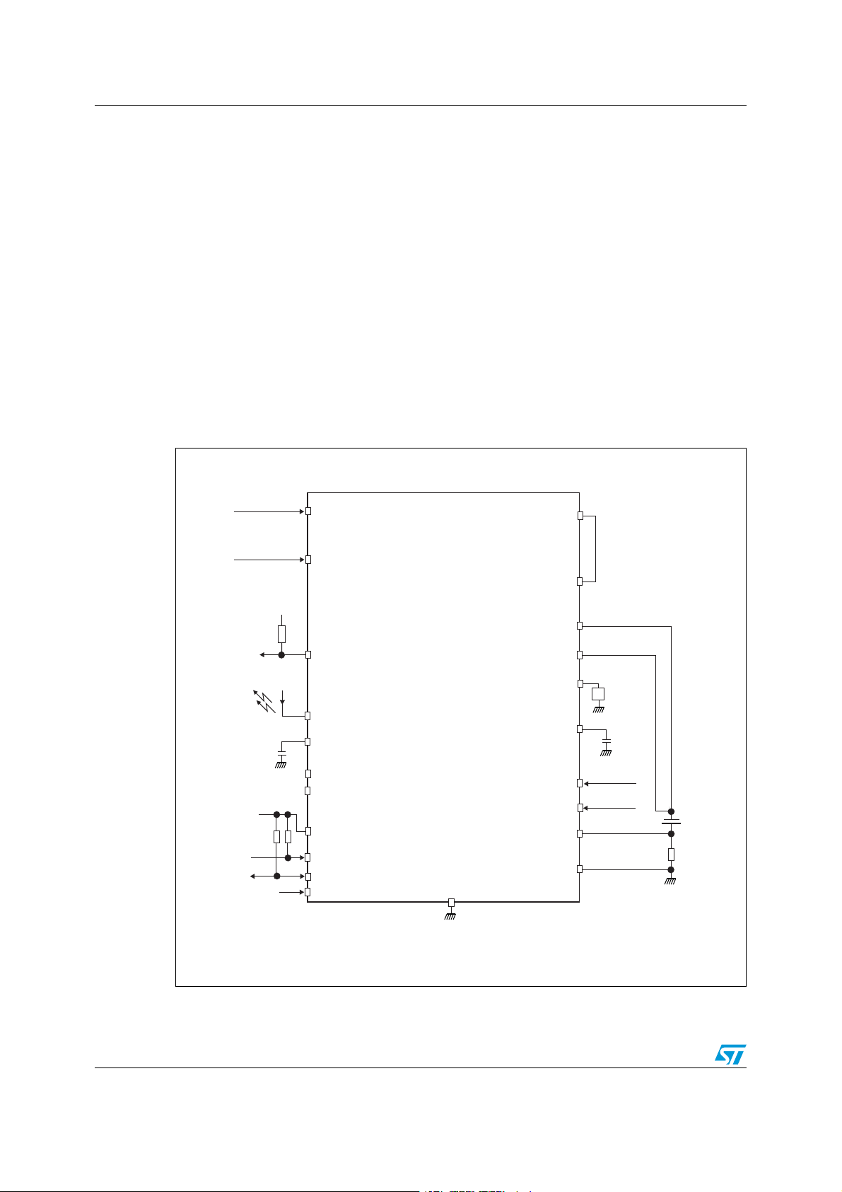
A typical application of the STw4102 is shown in Figure 1.
Figure 1. Typical application diagram for the STw4102
TO$""
)NDICATOR,%$
2ESET
)/VOLTAGE
#
)/VOLTAGE
-!).
53"072
072$%4%#4.
%/#('
#62%&
,$/$26
,$/&"
6)/
3#,
3$!
2%3%4.
34W
'.$
6/54
3%.3%
"!44
"!443%.3%
)3%4
#6)3
#+(:
34$"9
)#'
)#'
2
#
K(Z
3TAND"Y
2
2/16
!-
Page 3

AN2831 About the STw4102
The STw4102 mode and operation are controlled through an I2C interface. The VIO voltage
is the supply voltage for the digital I/Os.
● SCL and SDA are the clock and data signals of the I2C interface.
● RESETN is used to reset the STw4102 registers to their default value.
● C32KHZ is a 32,768 Hz clock signal used as a time base for the gas gauge.
● STDBY may be used to put the battery monitoring functions in standby mode by using
a hardware signal, the standby state is controlled by a combination of the STDBY
signal and the CG_ENA and ADPOWERON bits in the internal registers. If not used,
the STDBY pin must be connected to VIO.
Refer to the STw4102 datasheet for more detailed information
(a)
.
a. See Table 7: Document references.
3/16
Page 4
General control flow chart AN2831
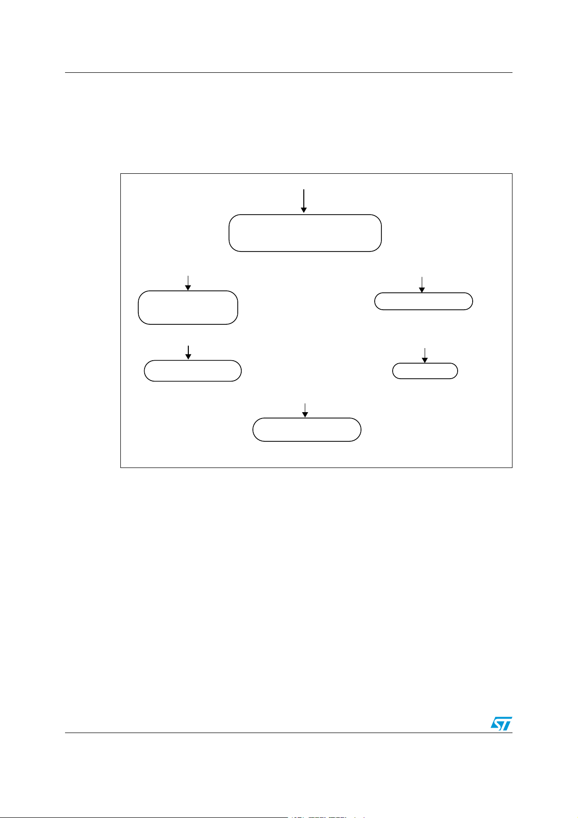
2 General control flow chart
Figure 2 depicts the general flow chart to control the charge and battery monitoring
functions of the STw4102.
Figure 2. General charge and battery monitoring flow chart
!PPLICATIONSTA
ZETHECHARGEPARAMETERS
)NITIALI
3TARTTHEGASGAUGESYSTEM
3ETUPAPE
RIODTASKh'AS'AUGEv
RTUP
0ERIODTASK@'AS'AUGE
2EADGASGAUGE
2EADBATTERYVOLTAGE
2EFRESHWATCHDOG
0/7%2$%4%#4.FALLINGEDGE
3TARTOFCHARGE
3ETUPTHECHARGETIMER
!PPLICATIONSHUTDOWN
)FCHARGINGSTOPCHARGING
3TOPGASGAUGE
53"STATUSCHANGE
5PDATECHARGECURRENT
0/7%2$%4%#4.RISINGEDGE
ORCHARGETIMERELAPSED
The controller tasks are described in detail in the following sections.
%NDOFCHARGE
!-
4/16
Page 5

AN2831 Charge function
3 Charge function
The STw4102 charge function is designed to be controlled by the application system
controller. However, if the controller is not active (for instance when the battery is fully
discharged) the STw4102 operates in standalone mode.
When the system is in the power-down state, the supplies are usually switched off and VIO
is not present. In this case, all the I/O lines, especially the RESETN signal, are low and the
control registers are automatically reset to the default values. The STw4102 starts charging
as soon as a power source is connected to the MAIN or USBPWR inputs.
3.1 Power-up conditions
The charge is enabled at power-up so as to be able to charge an empty battery when the
controller is unable to start due to the battery voltage being too low.
In the standard configuration, the power-up conditions are as follows.
● The charge voltage is set to 4.1 V to ensure maximum safety with all kinds of Li-Ion
batteries.
● The MAIN input is in the wall adapter mode, meaning that the charge current is set by
the external resistor; this corresponds to a configuration where the wall adapter and
USB cable use separate inputs.
● The USB charge current is set to 60 mA to comply with the USB 2.0 regulation.
● The watchdog is enabled and is set to one minute.
For special requirements (for instance, if the STw4102 is used in the common wall
adapter/USB input mode) and on request, some power-up values can be changed directly at
factory level.
● MAIN input mode: either wall adapter mode or USB mode.
● Watchdog enable or disabled: period = 1, 15, 30 or 60 minutes.
Refer to chapter 9 of the STw4102 datasheet for all factory options
(b)
.
When the system controller starts, it has to set the appropriate charge parameters.
● Charge voltage: usually 4.2 V for most batteries. The 4.1 V setting can be used to
extend battery lifetime but with reduced capacity. New high performance battery
generations may take benefit of the 4.30 and 4.35 V settings (consult battery
datasheets).
● MAIN input mode, if different from the power-up mode.
● USB current capability depending on the USB state: 0, 60 or 400 mA.
● Watchdog delay: it is recommended to keep the watchdog enabled and set to 1 minute
for maximum charge safety. If the watchdog is not used it must be disabled with
WDOG_EN=0 and cleared with WDOG_RST=1.
This is done by accessing the REG_CHG0 and REG_WDOG registers. The charge
parameters are kept in the STw4102 registers until the RESETN signal goes low.
b. See Table 7: Document references.
5/16
Page 6

Charge function AN2831
The open-drain PWRDETECTN output indicates that a power source is plugged in (wall
adapter or USB cable). This output can be used to wake up the system, or signal the event
by an interrupt mechanism. The MAINDETECT and USBDETECT bits in the REG_CHG0
register can be used to determine which power source is plugged in.
3.2 Controller tasks during the charge
While the application is active, the controller manages the following tasks.
● When a power source is detected, the controller starts a new charge cycle according to
the actual power source.
● When charging from a USB port, the controller sets the appropriate charge current
level or even disables the charge according to the current USB state.
● When the charge duration reaches the maximum charge time (usually 3 hours when
using fast charge from a wall adapter), the controller disables the STw4102 charge
function.
The watchdog must be refreshed periodically to keep the charge active. If the watchdog
period elapses, then the charge is disabled until the watchdog is refreshed again. Note that
if the watchdog elapses and then is disabled, the charge is still disabled. The suggested
method is to manage the watchdog as part of the battery monitoring and gas gauge task
(see Chapter 4: Battery monitoring functions).
Enabling and disabling the charge is done with the CHG_ENA bit in the REG_CHG1
register. When the charge is active, the EOCHG open-drain output indicates the charge
status: EOCHG is pulled down when the STw4102 is the fast charge phase and is open near
the end of charge when the charge current is less than 10% of the programmed charge
current. The same information is available with the CHARGERUN bit in the REG_CHG0
register. Note that an open EOCHG state does not necessarily mean that the charge is
finished, it just indicates to the user that the battery is almost fully charged, but the STw4102
continues to charge the battery to optimize the final stored energy (top-off or maintenance
phase). EOCHG can be forced low, for instance during the complete charge duration, by
writing to the FORCECHARGERUN bit in the REG_CHG1 register.
The system controller must stop the charge, usually 3 hours after the charge start. An
alternative method that does not involve the controller is to set the watchdog period to one
hour after EOCHG goes high and let the watchdog stop the charge. In all cases, it is not
recommended to keep the battery charging for long periods as this can reduce the battery’s
lifetime.
6/16
Page 7

AN2831 Charge function
3.3 Separate wall adapter/USB input configuration
Figure 3. STw4102 used in dual input mode
7ALLADAPTER
#
53"CABLE
#
-!).
53"072
34W
!-
In this configuration, the REG_CHG0 register must be programmed with SEL_DC_USB=0,
which is the standard power-up value. The STw4102 then automatically uses the MAIN or
USBPWR input according to the internal logic, which gives priority to the MAIN input if the
two inputs are connected to power sources.
There can be some cases where the USB charge must be disabled, like for instance when
the USB is used for OTG purposes. Two possibilities exist.
● If the USBPWR input standby current must be reduced to a minimum, then the charge
must be globally disabled for both MAIN and USBPWR inputs by setting the CHG_ENA
bit to 0. The USBPWR standby current is then reduced to 40 µA maximum.
● If a higher standby current on the USBWR input is acceptable, then the charge from the
MAIN input can still be enabled: CHG_ENA is set to 1, the USB current is set to 0 by
setting both USB_ICHG bits to 1 and the special SEL_IS bit in the REG_CHG1 register
is set to 1. In this case the USB standby input current is approximately 250 µA.
3.4 Common wall adapter/USB input configuration
Figure 4. STw4102 used in common input mode
7ALLADAPTER
-!).
#
53"CABLE
53"072
7/16
34W
!-
Page 8

Charge function AN2831
In this configuration, the MAIN input is used for charging from either a wall adapter, a
dedicated USB charger that allows more than 500 mA or a USB 2.0 cable limited to 500 mA.
In this case the SEL_DC_USB and USB_ICHG bits are used to set the charge current
according to the actual power source connected to the MAIN input:
● USB cable, 100 mA capability: set SEL_DC_USB=1, USB_ICHG=00.
● USB cable, 500 mA capability: set SEL_DC_USB=1, USB_ICHG=10.
● dedicated USB charger, wall adapter: SEL_DC_USB=0, the charge current is then set
by the external resistance.
In this configuration, when the charge is disabled with the CHG_ENA bit set to 0, the MAIN
input current is approximately 2 mA.
8/16
Page 9

AN2831 Battery monitoring functions
4 Battery monitoring functions
The STw4102’s battery monitoring functions include:
● a gas gauge for automatic computation of the battery charge variation: this is done by
integrating the battery current versus the time and accumulating the resulting charge
into charge and discharge registers. The last measurement of the current is available.
● measurement of the battery voltage.
The battery monitoring functions are disabled when the system is in power-down state (VIO
off, RESETN low). This ensures a low standby current from the battery.
The gas gauge function uses a 13-bit ADC and is enabled by the CG_ENA bit in the
REG_CG register. Once enabled, the gas gauge continuously updates the battery current
measurement and the charge/discharge internal registers.
4.1 Charge and discharge data reading
The charge and discharge data as well as the conversion count are read at the request of
the system controller by using the RD_REQ bit. The recommended procedure is:
● set RD_REQ.
● wait for 250 µs.
● read the locations REG_CHARGE (3 bytes), REG_DISCHARGE (3 bytes) and
REG_CONVNUMBER (2 bytes).
The charge/discharge values depend on the external resistance Rsense:
● Charge data (mA.h) = 0.00163 µV.h * REG_CHARGE / Rsense (mΩ).
● Discharge data (mA.h) = 0.00163 µV.h * REG_DISCHARGE / Rsense (mΩ).
When an accumulator reaches its maximum value (binary code = 2
stops accumulating. It is important to periodically reset the accumulators with the
RST_CHRG and RST_DCHG bits. The conversion counter does not stop when it reaches
12
2
-1 = 0xFFF, but wraps to 0 and continues counting. It may, however, be convenient to
reset it with the RST_COUNTER bit at the same time as the accumulators. Note that the
conversion counter is 12 bits wide and that the upper 4 bits of the high byte must be
discarded.
The CG_EOC bit in the REG_CG register can be used to check if at least one new
conversion has been made since the last reading of REG_CG.
4.2 Battery current reading
The last measured value of the current is available in the CONVDATA locations (2 bytes), is
updated at each conversion and is not synchronized with the I2C. To read it:
● read the CONVDATA (2 bytes) location once.
● read again the CONVDATA location.
● if the two results do not match, read the CONDATA location a third time.
The actual value of the current depends on the value of the external sense resistor:
Current (mA) = CONVDATA * 23.5 µV / Rsense (mΩ).
24
-1 = 0xFFFFFF), it
9/16
Page 10

Battery monitoring functions AN2831
4.3 Battery voltage reading
The voltage measurement uses a separate 7- or 12-bit analog-to-digital converter (ADC)
that operates independently of the current measurement and gas gauge. The 7-bit mode
gives the shortest conversion time (8 ms) whereas the 12-bit mode gives full resolution
(1.4 mV). The resolution is set by the ADRESOLUTION bits. Generally, the 12-bit mode
should be used, unless fast battery voltage variations have to be monitored.
The battery voltage measurement is made under control of the system controller: the ADC
must be enabled by setting the ADPOWERON bit and each conversion has to be triggered
by setting the ADSTART bit in the REG_ADCTRL register.
The recommended read procedure is:
● at power up, initialize the ADC by setting ADPOWERON, and trigger a first conversion
by setting the ADSTART bit.
● periodic task: read the battery voltage at the REG_ADDATA location (1 byte in 7-bit
resolution, 2 bytes in 12-bit resolution), then trigger the next conversion by setting again
the ADSTART bit.
In this way, the last voltage result is always available. The LSB value is 45.4 mV in 7-bit
resolution and 1.42 mV in 12-bit resolution.
4.4 Controller tasks
The gas gauge and voltage measurement functions are disabled at power-up or at each
STw4102 reset (RESETN input driven to low level).
The system controller does the following tasks.
● At start-up, it enables the gas gauge and the ADC for battery voltage measurement.
● It periodically reads the gas gauge and battery voltage, and if necessary resets the
accumulators.
● At power-down, it disables the gas gauge and battery voltage ADC.
Note: 1 The 32768 Hz clock signal must be present for both the gas gauge and battery voltage
measurement functions. When the gas gauge and battery voltage ADC are stopped with the
CG_ENA and ADPOWERON bits, the clock signal must still be present until the end of the
current conversion (this can take up to 250 ms).
2 If the battery voltage ADC is not used, the ADPOWERON bit must still be set at start-up and
cleared at power-down. This ensures correct operation of the standby mode of the STw4102
and minimum quiescent current from the battery.
10/16
Page 11

AN2831 STw4102 demonstration board
Appendix A STw4102 demonstration board
The STw4102 demonstration board is convenient to evaluate the charge and battery
monitoring functions and quickly obtain a working prototype or design reference.
Figure 5 describes the basic connections to use the STw4102 demonstration board.
Figure 5. STw4102 demonstration board usage
Power Detected
Power Detected
Charging
Charging
(if R1 removed)
(if R1 removed)
STw4102
STw4102
Vdc
Vdc
Gnd
Gnd
VBUS
VBUS
Gnd
Gnd
Adapter
Adapter
(5V DC)
(5V DC)
Vio
Vio
System
System
Controller
Controller
Gnd
Gnd
| Battery +
| Battery +
The EOCH and PWRDT pads are connected to the STw4102 EOCHG and
POWERDETECTN pins respectively. The PWRDT pad has a 10 kΩ pull-up resistor to BATT.
The demonstration board is configured for a charge current of 1 A from the MAIN wall
adapter set by the R1 resistor on the board. To change the charge current, remove the R1
resistor from the board and use an external resistor between the ISET pad and ground.
The gas gauge sense resistor is on the board and the resistance value is 33 mΩ.
The digital interface is made of VIO (I/O voltage to be externally provided, 1.45 to 3.0 V),
SDA, SCL (I2C bus signals), RST (STw4102 RESETN), STBY (STw4102 STDBY) and C32
(STw4102 C32KHZ). The RST pad has a 10 kΩ pull-up resistor to VIO.
11/16
Page 12

STw4102 register mapping AN2831
Appendix B STw4102 register mapping
The mapping of all registers is shown in Tab le 1 .
Table 1. Register map
Name
REG_CHG0 0 R/W Charge control and status
REG_CHG1 1 R/W Charge enable
REG_WDOG 2 R/W Watchdog control
REG_CG 3 R/W Gas gauge control
REG_CHARGE_LOW 4 R Gas gauge charge data, bits 0-7
REG_CHARGE_MID 5 R Gas gauge charge data, bits 8-15
REG_CHARGE_HIGH 6 R Gas gauge charge data, bits 16-23
REG_DISCHARGE_LOW 7 R Gas gauge discharge data, bits 0-7
REG_DISCHARGE_MID 8 R Gas gauge discharge data, bits 8-15
REG_DISCHARGE_HIGH 9 R Gas gauge discharge data, bits 16-23
REG_CONVDATA_LOW 16 R Gas gauge AD converter data, bits 0-7
REG_CONVDATA_HIGH 17 R Gas gauge AD converter data, bits 8-12
REG_CONVNUMBER_LOW 18 R Number of conversions, bits 0-7
REG_CONVNUMBER_HIGH 19 R
REG_ADCTRL 20 R/W Battery voltage monitor control
REG_ADDATA_LOW 21 R Battery voltage data, bits 0-7
REG_ADDATA_HIGH 22 R Battery voltage data, bits 8-11 in 12-bit mode
Address
(dec.)
Type Description
Number of conversions, bits 8-11,
bits 12-15 are undefined
The registers REG_CHG0, REG_CHG1, REG_WDOG, REG_CG and REG_ADCTRL are
described in detail in Ta bl e 2 to Tab le 6 . Power-up values are set at power startup or at reset
(RESETN pin at low level).
12/16
Page 13

AN2831 STw4102 register mapping
Table 2. REG_CHG0. address 0 (00h)
Name Pos. Type
CHARGERUN 0 R 0
Power-
up
Description
0: charge is below 10% of fast charge current.
1: charge is above 10% of fast charge current.
MAINDETECT 1 R 0 Main input voltage detection.
USBDETECT 2 R 0 USB input voltage detection.
VCHG [4,3] R/W 00
Charge voltage
00=4.1V, 01=4.2V, 10=4.3V, 11=4.35V.
Wall adapter/USB selection for MAIN input.
SEL_DC_USB 5 R/W 0
0: charge current set by Rset resistor.
1: charge current set by USB_ICHG bits.
USB_ICHG [7,6] R/W 00
Table 3. REG_CHG1. address 1 (01h)
Name Pos. Type
Power-
CHG_ENA 0 R/W 1
USB charge current
00 = 60 mA, 01 = 200 mA, 10 = 400 mA, 11 = off.
up
Description
0: charger disabled.
1: charger enabled.
Reserved [3,1] R/W 0 Reserved bits, to be set to zero.
FORCECHARGER
UN
4R/W0
0: no effect.
1: force EOCHG low independently of charge
state.
0: internal supply from Main or USB input when
SEL_IS 5 R/W 0
available and charge enabled.
1: internal supply always from battery.
Unused [7,6] R/W
Table 4. REG_WDOG. address 2 (02h)
Name Pos. Type
WDOG_EN 0 R/W 1
WDOG_TIME [2,1] R/W 00
Power-
up
Description
0: watchdog disabled.
1: watchdog enabled.
00 = 1 minute, 01 = 15 minutes, 10 = 30 minutes,
11 = 60 minutes.
0: no effect.
WDOG_RST 3 R/W 0
1: reset watchdog. Bit cleared after watchdog
reset.
Reserved [5,4] R/W 0 Reserved bits, to be set to zero.
WDOG_INT 6 R x 1: watchdog has elapsed.
Unused 7
13/16
Page 14

STw4102 register mapping AN2831
Table 5. REG_CG. address 3 (03h)
Name Pos. Type
Power-
up
CG_ENA 0 R/W 0
RST_CHRG 1 R/W 0
RST_DCHRG 2 R/W 0
RST_COUNTER 3 R/W 0
RD_REQ 4 R/W 0
CG_CAL 5 R/W 0
CG_EOC 6 R 0
Unused 7
Table 6. REG_ADCTRL. address 20 (14h)
Description
0: gas gauge disabled. Charge/discharge
accumulators are reset.
1: gas gauge enabled.
0: no effect.
1: resets the charge accumulator. This bit auto
clears after the charge register has been reset.
0: no effect.
1: resets the discharge accumulator. This bit auto
clears after the discharge register has been reset.
0: no effect.
1: resets the counter conversion. This bit auto
clears after the counter register has been reset.
0: no effect.
1: transfers the 24-bit charge/discharge
accumulators and the conversion counter to the
charge/discharge and conversion number
registers. This bit auto clears after the transfer.
0: no effect.
1: allows calibration of the AD converter.
Set to high at the end of a conversion. Cleared
after a read.
Name Pos. Type
Power-
up
ADPOWERON 0 R/W 0
ONSTATE 1 R 0
ADSTART 2 R/W 0
ADRUN 3 R 0
ADRESOLUTION 4 R/W 0
ADCAL 5 R/W 0
Unused [7,6]
Description
0: allows ADC shutdown.
1: enables ADC operation.
0: ADC is not ready for operation.
1: ADC is ready for operation.
0: no effect.
1: allows to start a conversion. Cleared upon
writing.
0: an AD conversion is not running.
1: an AD conversion is running.
0: 7 bits.
1: 12 bits.
0: no effect.
1: allows calibration of the AD converter.
14/16
Page 15

AN2831 References
References
Table 7. Document references
Document
STw4102 - Dual USB/wall adapter Li-Ion battery charger with gas gauge (stw4102.pdf).
Revision history
Table 8. Document revision history
Date Revision Changes
23-Oct-2008 1 Initial release.
15/16
Page 16

AN2831
Please Read Carefully:
Information in this document is provided solely in connection with ST products. STMicroelectronics NV and its subsidiaries (“ST”) reserve the
right to make changes, corrections, modifications or improvements, to this document, and the products and services described herein at any
time, without notice.
All ST products are sold pursuant to ST’s terms and conditions of sale.
Purchasers are solely responsible for the choice, selection and use of the ST products and services described herein, and ST assumes no
liability whatsoever relating to the choice, selection or use of the ST products and services described herein.
No license, express or implied, by estoppel or otherwise, to any intellectual property rights is granted under this document. If any part of this
document refers to any third party products or services it shall not be deemed a license grant by ST for the use of such third party products
or services, or any intellectual property contained therein or considered as a warranty covering the use in any manner whatsoever of such
third party products or services or any intellectual property contained therein.
UNLESS OTHERWISE SET FORTH IN ST’S TERMS AND CONDITIONS OF SALE ST DISCLAIMS ANY EXPRESS OR IMPLIED
WARRANTY WITH RESPECT TO THE USE AND/OR SALE OF ST PRODUCTS INCLUDING WITHOUT LIMITATION IMPLIED
WARRANTIES OF MERCHANTABILITY, FITNESS FOR A PARTICULAR PURPOSE (AND THEIR EQUIVALENTS UNDER THE LAWS
OF ANY JURISDICTION), OR INFRINGEMENT OF ANY PATENT, COPYRIGHT OR OTHER INTELLECTUAL PROPERTY RIGHT.
UNLESS EXPRESSLY APPROVED IN WRITING BY AN AUTHORIZED ST REPRESENTATIVE, ST PRODUCTS ARE NOT
RECOMMENDED, AUTHORIZED OR WARRANTED FOR USE IN MILITARY, AIR CRAFT, SPACE, LIFE SAVING, OR LIFE SUSTAINING
APPLICATIONS, NOR IN PRODUCTS OR SYSTEMS WHERE FAILURE OR MALFUNCTION MAY RESULT IN PERSONAL INJURY,
DEATH, OR SEVERE PROPERTY OR ENVIRONMENTAL DAMAGE. ST PRODUCTS WHICH ARE NOT SPECIFIED AS "AUTOMOTIVE
GRADE" MAY ONLY BE USED IN AUTOMOTIVE APPLICATIONS AT USER’S OWN RISK.
Resale of ST products with provisions different from the statements and/or technical features set forth in this document shall immediately void
any warranty granted by ST for the ST product or service described herein and shall not create or extend in any manner whatsoever, any
liability of ST.
ST and the ST logo are trademarks or registered trademarks of ST in various countries.
Information in this document supersedes and replaces all information previously supplied.
The ST logo is a registered trademark of STMicroelectronics. All other names are the property of their respective owners.
© 2008 STMicroelectronics - All rights reserved
STMicroelectronics group of companies
Australia - Belgium - Brazil - Canada - China - Czech Republic - Finland - France - Germany - Hong Kong - India - Israel - Italy - Japan -
Malaysia - Malta - Morocco - Singapore - Spain - Sweden - Switzerland - United Kingdom - United States of America
www.st.com
16/16
 Loading...