

Page 1
AN2829
Application note
Dual step-down controller with auxilary voltages for
notebook system power
Introduction
The PM6681A is a dual step-down controller with adjustable output voltages that can be
used in notebook power syst ems. This demonst ration board re presents a t ypical applica tion
circuit. The PM6681A demonstration board allows testing of all funct ion s of th e device and
provides two switching sections, with (typ.) 1.5 V (OUT1) and 1.05 V (OUT2) outputs from
5.5 V to 28 V input battery voltage. The typical operating switching frequency of the two
sections is 200 kHz/300 kHz, respectively. Each switching section delivers more than 5 A of
output current. An internal linear regulator provides a fixed 5 V output voltage. Another
internal linear regulator provides an adjustable output voltage (default 3.3 V). Both linear
regulators can deliver up to 100 mA peak current.
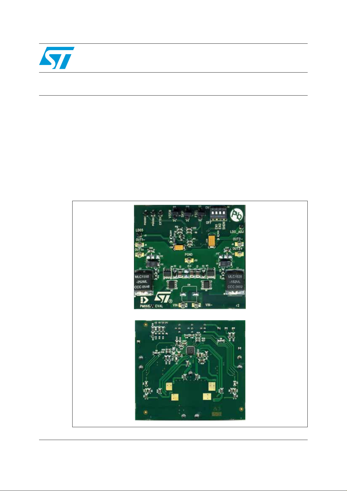
Figure 1. PM6681A demonstration board
AM01407v1
February 2009 Rev 1 1/32
www.st.com
Page 2

Contents AN2829
Contents
1 Main features . . . . . . . . . . . . . . . . . . . . . . . . . . . . . . . . . . . . . . . . . . . . . . . 4
2 Applications . . . . . . . . . . . . . . . . . . . . . . . . . . . . . . . . . . . . . . . . . . . . . . . . 5
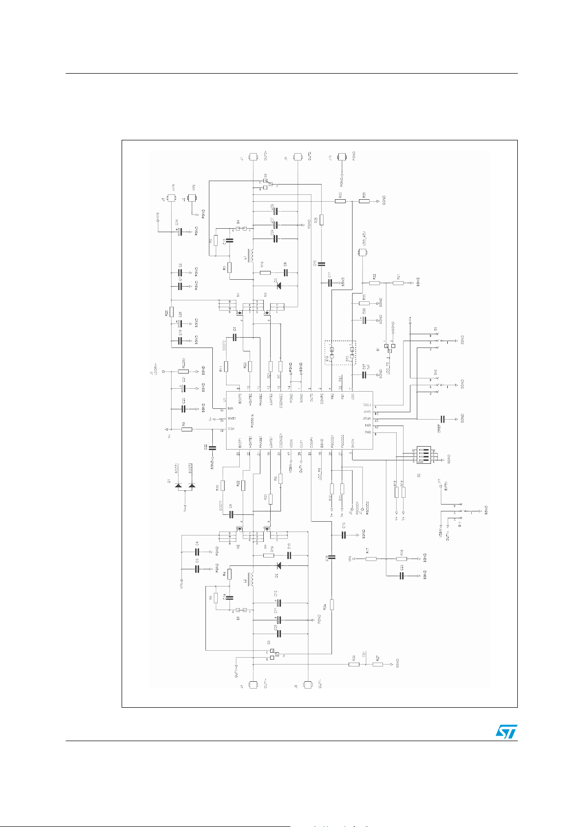
3 Demonstration board schematic . . . . . . . . . . . . . . . . . . . . . . . . . . . . . . . 6
4 Component list . . . . . . . . . . . . . . . . . . . . . . . . . . . . . . . . . . . . . . . . . . . . . 7
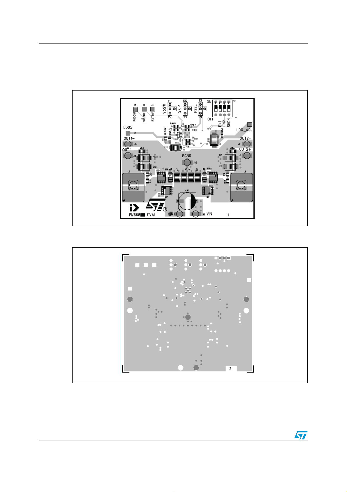
5 Demonstration board layout . . . . . . . . . . . . . . . . . . . . . . . . . . . . . . . . . . 10
6 I/O interface . . . . . . . . . . . . . . . . . . . . . . . . . . . . . . . . . . . . . . . . . . . . . . . 12
7 Recommended equipment . . . . . . . . . . . . . . . . . . . . . . . . . . . . . . . . . . . 13
8 Quick start . . . . . . . . . . . . . . . . . . . . . . . . . . . . . . . . . . . . . . . . . . . . . . . . 14
9 Jumper settings . . . . . . . . . . . . . . . . . . . . . . . . . . . . . . . . . . . . . . . . . . . . 15
10 Feedback output connections . . . . . . . . . . . . . . . . . . . . . . . . . . . . . . . . 17
11 Test setup and performance summary . . . . . . . . . . . . . . . . . . . . . . . . . 18
11.1 Test setup . . . . . . . . . . . . . . . . . . . . . . . . . . . . . . . . . . . . . . . . . . . . . . . . . 18
11.2 Power-up . . . . . . . . . . . . . . . . . . . . . . . . . . . . . . . . . . . . . . . . . . . . . . . . . 18
11.3 Soft-start and shutdown waveforms . . . . . . . . . . . . . . . . . . . . . . . . . . . . . 19
11.4 1.5 V and 1.05 output efficiency vs. load current . . . . . . . . . . . . . . . . . . . 21
11.5 Power consumption analysis . . . . . . . . . . . . . . . . . . . . . . . . . . . . . . . . . . 22
11.6 Switching frequency vs. load current . . . . . . . . . . . . . . . . . . . . . . . . . . . . 25
11.7 Linear regulator output voltages vs. output current . . . . . . . . . . . . . . . . . 26
11.8 Load transient response . . . . . . . . . . . . . . . . . . . . . . . . . . . . . . . . . . . . . . 27
12 Representative waveforms . . . . . . . . . . . . . . . . . . . . . . . . . . . . . . . . . . . 29
13 Revision history . . . . . . . . . . . . . . . . . . . . . . . . . . . . . . . . . . . . . . . . . . . 31
2/32
Page 3

AN2829 List of figures
List of figures
Figure 1. PM6681A demonstration board . . . . . . . . . . . . . . . . . . . . . . . . . . . . . . . . . . . . . . . . . . . . . . 1
Figure 2. Demonstration board schematic diagram. . . . . . . . . . . . . . . . . . . . . . . . . . . . . . . . . . . . . . . 6
Figure 3. PM6681A demonstration board layout - top layer (PGND plane and component side) . . . 10
Figure 4. PM6681A demonstration board layout - inner layer 1 (SGND layer and VIN plane) . . . . . 10
Figure 5. PM6681A demonstration board layout - inner layer 2 (SGND layer and signals). . . . . . . . 11
Figure 6. PM6681A demonstration board layout - bottom layer (PM6681A and component side) . . 11
Figure 7. Setup connections . . . . . . . . . . . . . . . . . . . . . . . . . . . . . . . . . . . . . . . . . . . . . . . . . . . . . . . 18
Figure 8. REF, LDO5 and LDO power-up . . . . . . . . . . . . . . . . . . . . . . . . . . . . . . . . . . . . . . . . . . . . . 19
Figure 9. Section 1 soft-start waveforms . . . . . . . . . . . . . . . . . . . . . . . . . . . . . . . . . . . . . . . . . . . . . . 20
Figure 10. Section 2 soft-start waveforms . . . . . . . . . . . . . . . . . . . . . . . . . . . . . . . . . . . . . . . . . . . . . . 20
Figure 11. Section 1 shutdown waveforms . . . . . . . . . . . . . . . . . . . . . . . . . . . . . . . . . . . . . . . . . . . . . 21
Figure 12. Section 2 shutdown waveforms . . . . . . . . . . . . . . . . . . . . . . . . . . . . . . . . . . . . . . . . . . . . . 21
Figure 13. 1.5 V SMPS efficiency . . . . . . . . . . . . . . . . . . . . . . . . . . . . . . . . . . . . . . . . . . . . . . . . . . . . 22
Figure 14. 1.05 V SMPS efficiency . . . . . . . . . . . . . . . . . . . . . . . . . . . . . . . . . . . . . . . . . . . . . . . . . . . 22
Figure 15. Input current vs. input voltage. . . . . . . . . . . . . . . . . . . . . . . . . . . . . . . . . . . . . . . . . . . . . . . 23
Figure 16. Input current vs. input voltage. . . . . . . . . . . . . . . . . . . . . . . . . . . . . . . . . . . . . . . . . . . . . . . 23
Figure 17. Input current vs. input voltage. . . . . . . . . . . . . . . . . . . . . . . . . . . . . . . . . . . . . . . . . . . . . . . 24
Figure 18. Device current consumption vs. input voltage . . . . . . . . . . . . . . . . . . . . . . . . . . . . . . . . . . 24
Figure 19. Device current consumption vs. input voltage . . . . . . . . . . . . . . . . . . . . . . . . . . . . . . . . . . 25
Figure 20. 1.5 V output switching frequency vs. load current . . . . . . . . . . . . . . . . . . . . . . . . . . . . . . . 25
Figure 21. 1.05 V output switching frequency vs. load current . . . . . . . . . . . . . . . . . . . . . . . . . . . . . . 26
Figure 22. LDO5 output vs. load current . . . . . . . . . . . . . . . . . . . . . . . . . . . . . . . . . . . . . . . . . . . . . . . 26
Figure 23. ADJ_LDO load regulation. . . . . . . . . . . . . . . . . . . . . . . . . . . . . . . . . . . . . . . . . . . . . . . . . . 27
Figure 24. SMPS 1.5 V load transient response . . . . . . . . . . . . . . . . . . . . . . . . . . . . . . . . . . . . . . . . . 27
Figure 25. SMPS 1.05 V load transient response . . . . . . . . . . . . . . . . . . . . . . . . . . . . . . . . . . . . . . . . 28
Figure 26. SMPS pulse skip mode. . . . . . . . . . . . . . . . . . . . . . . . . . . . . . . . . . . . . . . . . . . . . . . . . . . . 29
Figure 27. SMPS no-audible skip mode . . . . . . . . . . . . . . . . . . . . . . . . . . . . . . . . . . . . . . . . . . . . . . . 29
Figure 28. SMPS PWM mode . . . . . . . . . . . . . . . . . . . . . . . . . . . . . . . . . . . . . . . . . . . . . . . . . . . . . . . 30
3/32
Page 4

Main features AN2829
1 Main features
● 5.5 V to 36 V input voltage range
● Adjustable output voltages
● 0.9-3.3 V adjustable LDO delivers 100 mA peak current
● 5 V LDO delivers 100 mA peak current
● 1.237 V ±1% reference voltage available
● Lossless current sensing using low side MOSFET R
●
Negative current limit
● Soft-start internally fixed at 2 ms
● Soft output discharge
● Latched UVP
● Non-latched OVP
● Selectable pulse skipping at light loads
● Selectable minimum frequency (33 kHz) in pulse skip mode
● 4 mW maximum quiescent power
● Independent Power Good signals
● Output voltage ripple compensation.
DS(on)
4/32
Page 5

AN2829 Applications
2 Applications
● Notebook, tablet and slate computers
● Mobile system power supplies
● 3-4 cell Li+ battery-powered devices
5/32
Page 6
Demonstration board schematic AN2829
3 Demonstration board schematic
Figure 2. Demonstration board schematic diagram
6/32
AM01408v1
Page 7

AN2829 Component list
4 Component list
Table 1. Bill of materials
Qty Component Description Package Part number MFR Value
3C1:C3
1C4
2C5, C6
1C19
1C7
2C9, C10
1C11
1C8
1C12
2C13, C14
2C15, C16
Ceramic
capacitor
Ceramic
capacitor
Ceramic
capacitor
Ceramic
capacitor
POSCAP
capacitor
Ceramic
capacitor
POSCAP
capacitor
POSCAP
capacitor
POSCAP
capacitor
Ceramic
capacitor
Ceramic
capacitor
1812 UMK325BJ106KM-T Taiyo-Yuden 10 µF - 50 V
1812 NM 10 µF - 50
0805 100 nF - 50 V
0805 100 nF - 50 V
7343 NM Sanyo
0805 NM
7343 NM Sanyo
7343 6TPB330M Sanyo
7343 6TPB330M Sanyo
0603 5.6 nF - 50 V
0603 1 nF - 50 V
330 µF -
12 mR - 6 V
330 µF -
12 mR - 6 V
2C17, C18
1C20
1C21
1C22
1C23
1CIN
1 CREF
1C26
Ceramic
capacitor
Ceramic
capacitor
Tantalum
capacitor
Ceramic
capacitor
Ceramic
capacitor
Electrolytic
capacitor
Ceramic
capacitor
Tantalum
capacitor
0603 47 pF - 50 V
0805 1 µF - 10 V
3216 4.7 µF - 16 V
0805 220 nF - 10 V
0805 10 pF
D=10 mm NM
0805 100 nF - 50 V
6032 4.7 µF - 35 V
7/32
Page 8

Component list AN2829
Table 1. Bill of materials (continued)
Qty Component Description Package Part number MFR Value
1C24, C25
1C27
1C28
1D1
2D2, D3
1IC1
1 L1 Inductor
1 L2 Inductor
4M1:M4
1 R3 Resistor 0805 22 kΩ - 1%
1 R4 Resistor 0805 36 kΩ - 1%
1 R5 Resistor 0805 3.3 kΩ - 1%
Tantalum
capacitor
Tantalum
capacitor
Tantalum
capacitor
Dual schottky
diode
Diode 1 A -
30 V
PM6681A
device
MOSFET
control FET
0805 10 µF - 6.3 V
0805 10 µF - 6.3 V
3216 4.7 µF - 16 V
SOT23 BAT54A STMicroelectronics
DO216AA STPS1L30M STMicroelectronics
QFN-32 PM6681A STMicroelectronics
13 mm x
13 mm
13 mm x
13 mm
SO-8 STS12NH3LL
MLC1538-152ML Coilcraft 1.5 µH - 12 A
MLC1515-252ML Coilcraf 2.5 µH - 8 A
1 R6 Resistor 0805 3 kΩ - 1%
2 R7, R8 Resistor 0805 680 Ω - 1%
1 R9 Resistor 0805 47 Ω - 1%
2 R10, R11 Resistor 0805 10 Ω - 1%
4 R12:R15 Resistor 0805 100 kΩ - 1%
1 R16 Resistor 0805 150 kΩ - 1%
1 R17 Resistor 0805 560 kΩ - 1%
2 R18, R19 Resistor 0805 NM
R20, R21,
4
R22, R23
1 R24 Resistor 0805 1.1 kΩ - 1%
1 R25 Resistor 0805 820 Ω - 1%
1 R26 Resistor 1206 3.9 Ω - 1%
1 R27 Resistor 0805 10 kΩ - 1%
1 R29 Resistor 0805 11 kΩ - 1%
1 R28 Resistor 0805 6.8 kΩ - 1%
1 R30 Resistor 0805 1.8 kΩ - 1%
Resistor 0805 0 Ω - 1%
8/32
Page 9

AN2829 Component list
Table 1. Bill of materials (continued)
Qty Component Description Package Part number MFR Value
1 R31 Resistor 0603 5.6 kΩ - 1%
1 R32 Resistor 0603 15 kΩ - 1%
1
RLD5V,
RLD3V
Resistor 0805 NM
9/32
Page 10
Demonstration board layout AN2829
5 Demonstration board layout
Figure 3. PM6681A demonstration board layout - top layer (PGND plane and
component side)
AM01409v1
Figure 4. PM6681A demonstration board layout - inner layer 1 (SGND layer and VIN
plane)
AM01410v1
10/32
Page 11

AN2829 Demonstration board layout
Figure 5. PM6681A demonstration board layout - inner layer 2 (SGND layer and
signals)
AM01411v1
Figure 6. PM6681A demonstration board layout - bottom layer (PM6681A and
component side)
AM01412v1
11/32
Page 12

I/O interface AN2829
6 I/O interface
The demonstration board has the following test points:
Table 2. Demonstration board test points
Test point Description
V
+ Input voltage
IN
- Input voltage ground
V
IN
LDO5 5 V linear regulator output
LDO_ADJ Adjustable linear regulator output
EXT5V 5 V external input
OUT1+ OUT1 switching section output
OUT1- OUT1 switching section output ground
PGOOD1 OUT1 switching section Power Good
OUT2+ OUT2 switching section output
OUT2+ OUT2 switching section output ground
PGOOD2 OUT2 switching section Power Good
J10 Junction pin between PGND and SGND planes
12/32
Page 13

AN2829 Recommended equipment
7 Recommended equipment
● 5.5 V to 36 V power supply, notebook battery or AC adapter
● Active loads
● Digital multimeters
● 500 MHz four-trace oscilloscope
13/32
Page 14

Quick start AN2829
8 Quick start
1. Connect VIN+ and VIN- test points of the demonstration board to an external power
supply.
2. Ensure that all switches of DIP-switch "S2" are "OFF". In this condition all outputs are
disabled (shutdown-mode).
3. Turn "S21"on (SHDN pin high). The LDO5 and LDO_ADJ outputs turn-on (standbymode).
4. Turn "S22" on (EN1 pin high). The 1.5 V switching controller brings its output into
regulation. The PGood1 pin goes high after soft-start.
5. Turn "S23" on (EN2 pin high). The 1.05 V switching controller brings its output into
regulation. The PGood2 pin goes high after soft-start.
6. In order to load the switching outputs, loads must be connected between the "+" and
the "-" output test points, respe ctively.
7. In order to load the LDO5 linear output, loads m ust be connected between J10 and
LDO5 or resistor RLD5V can be mounted on the demonstration board.
8. In order to load the LDO_ADJ linear output, loads must be connect ed between J10 a nd
LDO_ADJ or the alternative resistor R33 can be mounted on the demonstration board.
14/32
Page 15

AN2829 Jumper settings
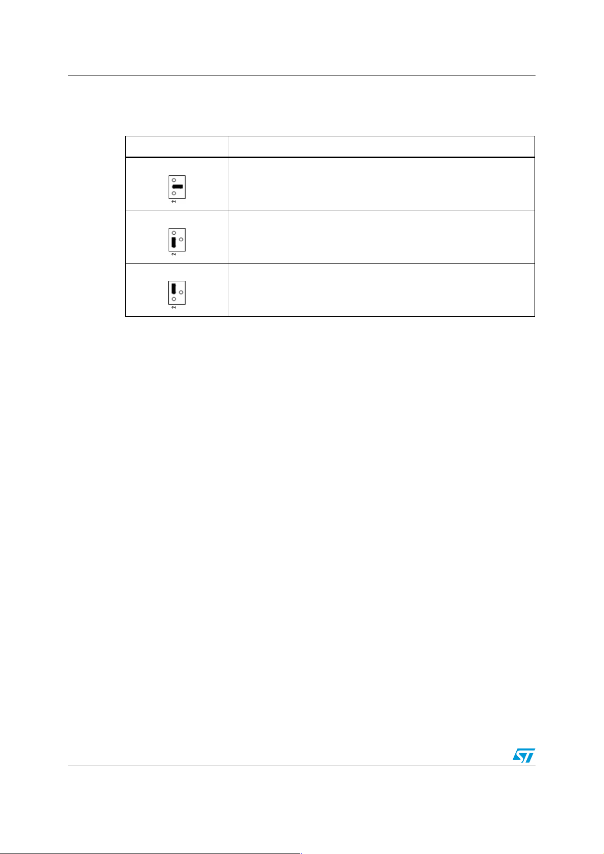
9 Jumper settings
It is possible to select different working conditions by using the jumpers:
Note: Please note that jumpers S1, S12 and S13 are already soldered on the demonstration
board, and it is not necessary to change them. Refer to the schematic to check their proper
connection.
● External bypass connections for the linear regulator LDO5(V5SW)
Table 3. Jumper S11 (connect V5SW pin to S11)
Position LDO5 working conditions
OUT5V
SGND
EXT5V
● SMPS frequency selection (FSEL)
When the main ouput voltage is greater than the bootstrap-switchover
threshold, an internal 3 Ω (max) P-channel MOSFET switch connects the
V5SW pin to the LDO5 pin, shutting down the LDO5 internal linear
regulator. If not used, it must be connected to ground.
The internal linear regulator LDO5 is always on. In this case LDO5
supplies all gate drivers and the internal circuitry. It can provide an output
peak current of 100mA.
The internal linear regulator LDO5 remains off if an alternative 5 V external
voltage is applied to the EXT5V test-point. An internal 3 Ω (max)
P-channel MOSFET switch connects the V5SW pin to the LDO5 output.
The gate drivers and internal circuitry are supplied by the same 5 V
external voltage applied.
Table 4. Jumper S3 (connect FSEL pin to S3)
Position SMPS OUT1 SMPS OUT2
SGND
200 kHz 325 kHz
VREF
LDO5
290 kHz 425 kHz
390 kHz 590 kHz
15/32
Page 16
Jumper settings AN2829
● SMPS mode selection (skip)
Table 5. Jumper S10 (connect SKIP pin to S10)
Position Switching operating mode
GND
VREF
LDO5
If the SKIP pin is tied to ground, pulse-skip mode occurs at light loads. A
zero crossing comparator prevents the inductor current from going
negative.
Connecting the SKIP pin to the VREF pin enables pulse skip mode with a
minimum switching frequency of approximately 25 kHz (ultrasonic mode).
If the SKIP pin is tied to 5 V, fixed PWM mode occurs. The switching output
is in a position to sink and source current from the load.
16/32
Page 17

AN2829 Feedback output connections
10 Feedback output connections
● Loop compensation network for very low output voltage ripple.
Table 6. Jumper S4, S5
Position Output ripple compensation
Short
Virtual ESR output ripple is generated by using a compensation network connected
between the output and the PHASE pin of the switching section.
Table 7. Jumper S8, S9
Position Feedback connection
Controller feedback signal connected to the compensation network.
● Loop compensation network for high output voltage ripple
Table 8. Jumper S4, S5
Position Output ripple compensation
Open ESR output ripple is used.
Table 9. Jumper S8, S9
Position Feedback connection
Controller feedback signal connected directly to the output capacitor.
17/32
Page 18

Test setup and performance summary AN2829
11 Test setup and performance summary
11.1 Test setup
The PM6681A demonstration board has the following input/output connections:
– 12 V input through J5-J2 (V
– 1.5 V SMPS output through J4-J13 (OUT1+ and OUT1-)
– 1.05 V SMPS output through J1-J12 (OUT2+ and OUT2-)
– 3.3 V linear regulator output through LDO_ADJ - J10
– 5 V linear regulator output through LDO5 - J3 (LDO5)
– A power supply capable of supplying at least 6 A should be connected to V
and two active loads should be connected respectively to OUT1+, OUT1- and
OUT2+, OUT2-.
Figure 7. Setup connections
+ and VIN-)
IN
+, VIN-
IN
11.2 Power-up
As shown in Figure 8, power-up starts when the input voltage is applied and the voltage on
the SHDN pin is above the device on threshold (1.5 V). First the LDO5 goes up with a
masking time of about 4 ms. If the LDO5 output is above the UVLO threshold at this time,
the device enters standby mode and the adjustable internal linear regulator LDO is turned
on.
18/32
AM01413v1
Page 19

AN2829 Test setup and performance summary
Figure 8. REF, LDO5 and LDO power-up
AM01414v1
11.3 Soft-start and shutdown waveforms
Figure 9, 10, 11 and 12 show, respectively, the soft-start and shutdown waveforms.
The PM681A has an independent internal digital soft-start for each switching section.
During the soft-start phase the internal current limit increases from 25% to 100% with steps
of 25% to avoid the inductor current rising abruptly.
19/32
Page 20

Test setup and performance summary AN2829
Figure 9. Section 1 soft-star t waveforms
OUT1
I_L
EN1
AM01415v1
Figure 10. Section 2 soft-start waveforms
OUT2
I_L
EN2
AM01416v1
Driving the EN1, EN2 pins below the EN off threshold (0.8 V), the switching outputs are
connected to ground through an internal 12 Ω P-MOSFET and are discharged gradually,
(discharge mode). When the output voltages reach 0.3 V, the low-side MOSFETs are turned
on, quickly discharging them to ground.
20/32
Page 21

AN2829 Test setup and performance summary
Figure 11. Section 1 shutdown waveforms
OUT1
Lgate1
EN1
AM01417v1
Figure 12. Section 2 shutdown waveforms
OUT2
Lgate2
EN2
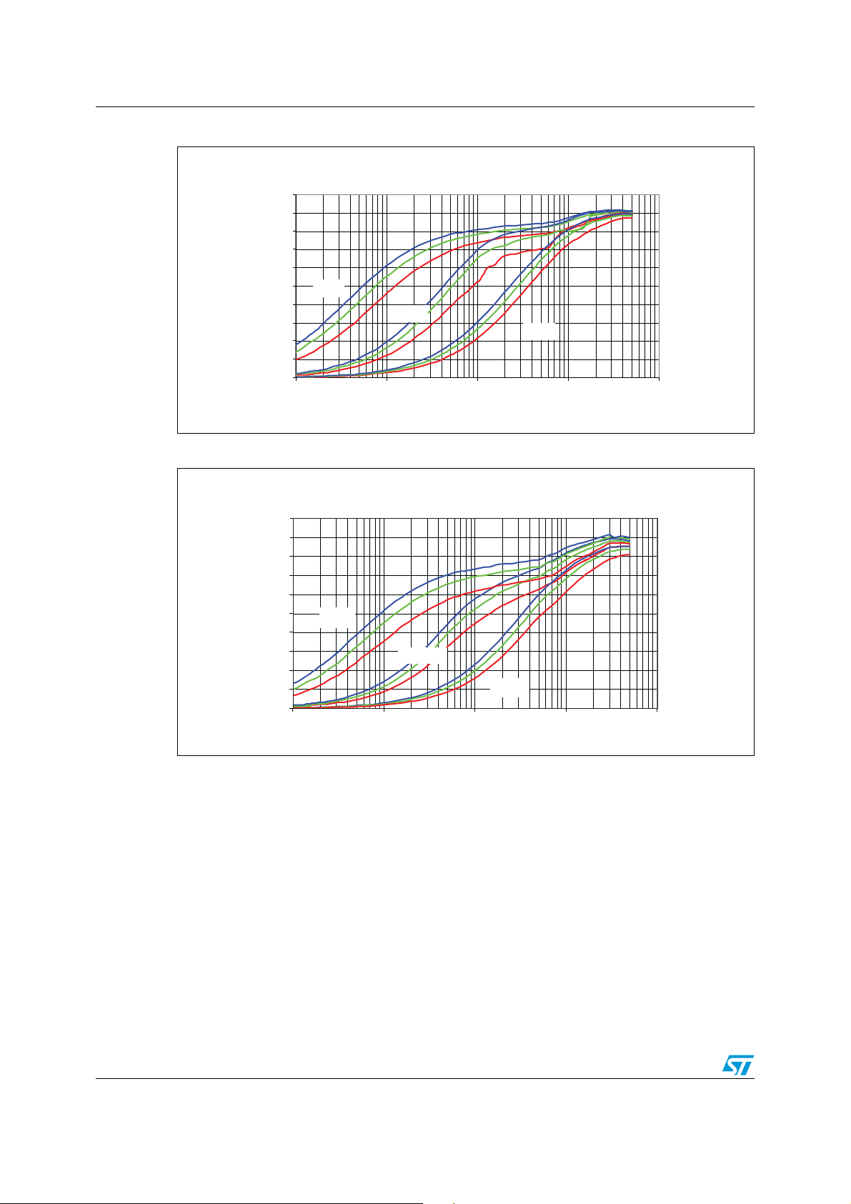
11.4 1.5 V and 1.05 output efficiency vs. load current
AM01418v1
Figure 13 and 14 show the efficiency versus load current at different input voltage values in
PWM mode, skip mode and no audib le skip mode. Three different input voltages are used:
● Blue: V
● Green: V
● Red: V
IN
=18 V
IN
=9 V
=12 V
IN
21/32
Page 22
Test setup and performance summary AN2829
Efficiency vs load current OUT1=1,5 V
0
10
20
30
40
50
60
70
80
90
100
0,001 0,010 0,100 1,000 10,000
Load current [A]
Efficiency [%]
Efficiency vs load curent OUT2=1,05 V
Laod current [A]
Figure 13. 1.5 V SMPS efficiency
SKIP
NASKIP
PWM
AM01419v1
Figure 14. 1.05 V SMPS efficiency
100
90
80
70
60
50
40
30
20
10
0
0,001 0,010 0,100 1,000 10,000
SKIP
11.5 Power consumption analysis
To measure the consumption of the device in real working conditions, an external power
supply of +5 V is connected to EXT5V.
The two traces on the following figures show the differentiation in the two input currents.
Once the internal linear regulator is turned on, the device consumption increases.
Figure 15 shows the input current consumption measured at V
the input device current consumption measured by the VCC pin. Both switching sections
work in forced PWM mode. No load is applied on the outputs.
22/32
NASKIP
PWM
AM01420v1
+ (including ISHDN) and
IN
Page 23

AN2829 Test setup and performance summary
PWM no load battery current
vs input voltage
5.00
10.00
15.00
20.00
25.00
30.00
35.00
8 10 12 14 16 18 20 22 24 26 28
Input voltage [V]
Input current [mA]
SKIP no load battery current
vs input voltage
0.00
0.10
0.20
0.30
0.40
0.50
0.60
8 10 12 14 16 18 20 22 24 26 28
Input voltage [V]
Input current [mA]
Figure 15. Input current vs. input voltage
linput
IEXT5V
AM01421v1
Figure 16 shows the input current consumption measured at V
+. Both switching sections
IN
work in pulse skip mode. No load is applied on the outputs.
Figure 16. Input current vs. input voltage
IEXT5V
Iinput
Figure 17 shows the input current consumption measured at V
work in no audible skip mode. No load is applied on the outputs.
AM01422v1
+. Both switching sections
IN
23/32
Page 24

Test setup and performance summary AN2829
Input voltage [V]
Input current [mA]
Input voltage [V]
Input current [uA]
Figure 17. Input current vs. input voltage
No-audible SKIP no load battery current
4.50
4.00
3.50
3.00
vs input voltage
Iinput
2.50
2.00
1.50
8 10 12 14 16 18 20 22 24 26 28
IEXT5V
AM01423v1
In the following figu res, the device current consumption is measured in shutdown mode. In
shutdown mode all outputs are off (SHDN pin low). In standby mode only the linear
regulators output are on (V5SW=SGND; SHDN pin high; EN5, EN3 pins low).
Figure 18. Device current consumption vs. input voltage
Shutdown mode input battery current
vs input voltage
30,00
25,00
20,00
15,00
10,00
5,00
0,00
8 10 12 14 16 18 20 22 24 26 2830 32 34 36
24/32
AM01424v1
Page 25

AN2829 Test setup and performance summary
Input voltage [V]
Input current [uA]
Figure 19. Device current consumption vs. input voltage
Standby mode input battery current
vs input voltage
380
360
340
320
300
280
260
240
8 10 12 14 16 18 20 22 24 26 2830 32 34 36
AM01425v1
11.6 Switching frequency vs. load current
Figure 20 and 21 show the switching frequency variation with the load current in PWM
mode, skip mode and no audible skip mode. 12 V is applied at the V
+ and VIN- test points.
IN
Figure 20. 1.5 V output switching frequency vs. load current
6 SWITCHINGFREQUENCYVSLOADCURRENT
3WITCHINGFREQUENCY;K(Z=
,OADCURRENT;!=
3+)0
07-
.!3+)0
!-V
25/32
Page 26

Test setup and performance summary AN2829
Figure 21. 1.05 V output switching frequenc y vs. load current
6SWITCHINGFREQUENCYVSLOADCURRENT
3WITCHINGFREQUENCY;K(Z=
,OADCURRENT;!=
3+)0
07-
.!3+)0
!-V
11.7 Linear regulator output voltages vs. output current
Figure 22 and 23 show the load regulation respectively for the internal linear regulators
LDO5 and the adjustable linear regulator LDO_ADJ. Both swit ching sections are disabled.
12 V is applied at the V
+ and VIN- test points.
IN
Figure 22. LDO5 output vs. load current
AM01428v1
26/32
Page 27

AN2829 Test setup and performance summary
Figure 23. ADJ_LDO load regulation
AM01429v1
11.8 Load transient response
The following figures show the load transient response from 1 A to 4 A for both switching
outputs. In both cases the PM6681A works in forced PWM mode (the SKIP pin is high).
Figure 24. SMPS 1.5 V load transient response
OUT1
I_L
VPhase
AM01430v1
27/32
Page 28

Test setup and performance summary AN2829
Figure 25. SMPS 1.05 V load transient response
OUT2
I_L
Vphase
AM01431v1
28/32
Page 29

AN2829 Representative waveforms
12 Representative waveforms
The following figu res show the relevant waveforms of a switching section, to underline the
behavior of the device in different working conditions: pulse skip mode, no-audible skip
mode and forced PWM mode.
Figure 26. SMPS pulse skip mode
Figure 27. SMPS no-audible skip mode
AM01432v1
AM01433v1
29/32
Page 30

Representative waveforms AN2829
Figure 28. SMPS PWM mode
AM01434v1
30/32
Page 31

AN2829 Revision history
13 Revision history
Table 10. Document revision history
Date Revision Changes
25-Feb-2009 1 Initial release
31/32
Page 32

AN2829
Please Read Carefully:
Information in this document is provided solely in connection with ST products. STMicroelectronics NV and its subsidiaries (“ST”) reserve the
right to make changes, corrections, modifications or improvements, to this document, and the products and services described herein at any
time, without notice.
All ST products are sold pursuant to ST’s terms and conditions of sale.
Purchasers are solely res ponsibl e fo r the c hoic e, se lecti on an d use o f the S T prod ucts and s ervi ces d escr ibed he rein , and ST as sumes no
liability whatsoever relati ng to the choice, selection or use o f the ST products and services desc ribed herein.
No license, express or implied, by estoppel or otherwise, to any intellectual property rights is granted under this document. If any part of this
document refers to any third pa rty p ro duc ts or se rv ices it sh all n ot be deem ed a lice ns e gr ant by ST fo r t he use of su ch thi r d party products
or services, or any intellectua l property c ontained the rein or consi dered as a warr anty coverin g the use in any manner whats oever of suc h
third party products or servi ces or any intellectual property contained therein.
UNLESS OTHERWISE SET FORTH IN ST’S TERMS AND CONDITIONS OF SALE ST DISCLAIMS ANY EXPRESS OR IMPLIED
WARRANTY WITH RESPECT TO THE USE AND/OR SALE OF ST PRODUCTS INCLUDING WITHOUT LIMITATION IMPLIED
WARRANTIES OF MERCHANTABILITY, FITNESS FOR A PARTICUL AR PURPOS E (AND THEIR EQUIVALE NTS UNDER THE LAWS
OF ANY JURISDICTION), OR INFRINGEMENT OF ANY PATENT, COPYRIGHT OR OTHER INTELLECTUAL PROPERTY RIGHT.
UNLESS EXPRESSLY APPROVED IN WRITING BY AN AUTHORIZED ST REPRESENTATIVE, ST PRODUCTS ARE NOT
RECOMMENDED, AUTHORIZED OR WARRANTED FOR USE IN MILITARY, AIR CRAFT, SPACE, LIFE SAVING, OR LIFE SUSTAINING
APPLICATIONS, NOR IN PRODUCTS OR SYSTEMS WHERE FAILURE OR MALFUNCTION MAY RESULT IN PERSONAL INJ URY,
DEATH, OR SEVERE PROPERTY OR ENVIRONMENTAL DAMAGE. ST PRODUCTS WHICH ARE NOT SPECIFIED AS "AUTOMOTIVE
GRADE" MAY ONLY BE USED IN AUTOMOTIVE APPLICATIONS AT USER’S OWN RISK.
Resale of ST products with provisions different from the statements and/or technical features set forth in this document shall immediately void
any warranty granted by ST fo r the ST pro duct or serv ice describe d herein and shall not cr eate or exten d in any manne r whatsoever , any
liability of ST.
ST and the ST logo are trademarks or registered trademarks of ST in various countries.
Information in this document su persedes and replaces all information previously supplied.
The ST logo is a registered trademark of STMicroelectronics. All other names are the property of their respective owners.
© 2009 STMicroelectronics - All rights reserved
STMicroelectronics group of compan ie s
Australia - Belgium - Brazil - Canada - China - Czech Republic - Finland - France - Germany - Hong Kong - India - Israel - Italy - Japan -
Malaysia - Malta - Morocco - Singapore - Spain - Sweden - Switzerland - United Kingdom - United States of America
www.st.com
32/32
 Loading...