

Page 1
AN2827
Application note
Driver for double flash LED with I²C interface
Introduction
This application note is dedicated to the design of a flash LED driver using the STCF05
device, which is a boost current mode converter with an I²C interface and internal current
source. The schematic, functional description, recommendations for PCB layout and
external components selection are also discussed in this application note. The STCF05
device is designed to drive two LEDs in series with a total forward voltage from 5.3 V to
10.2 V.
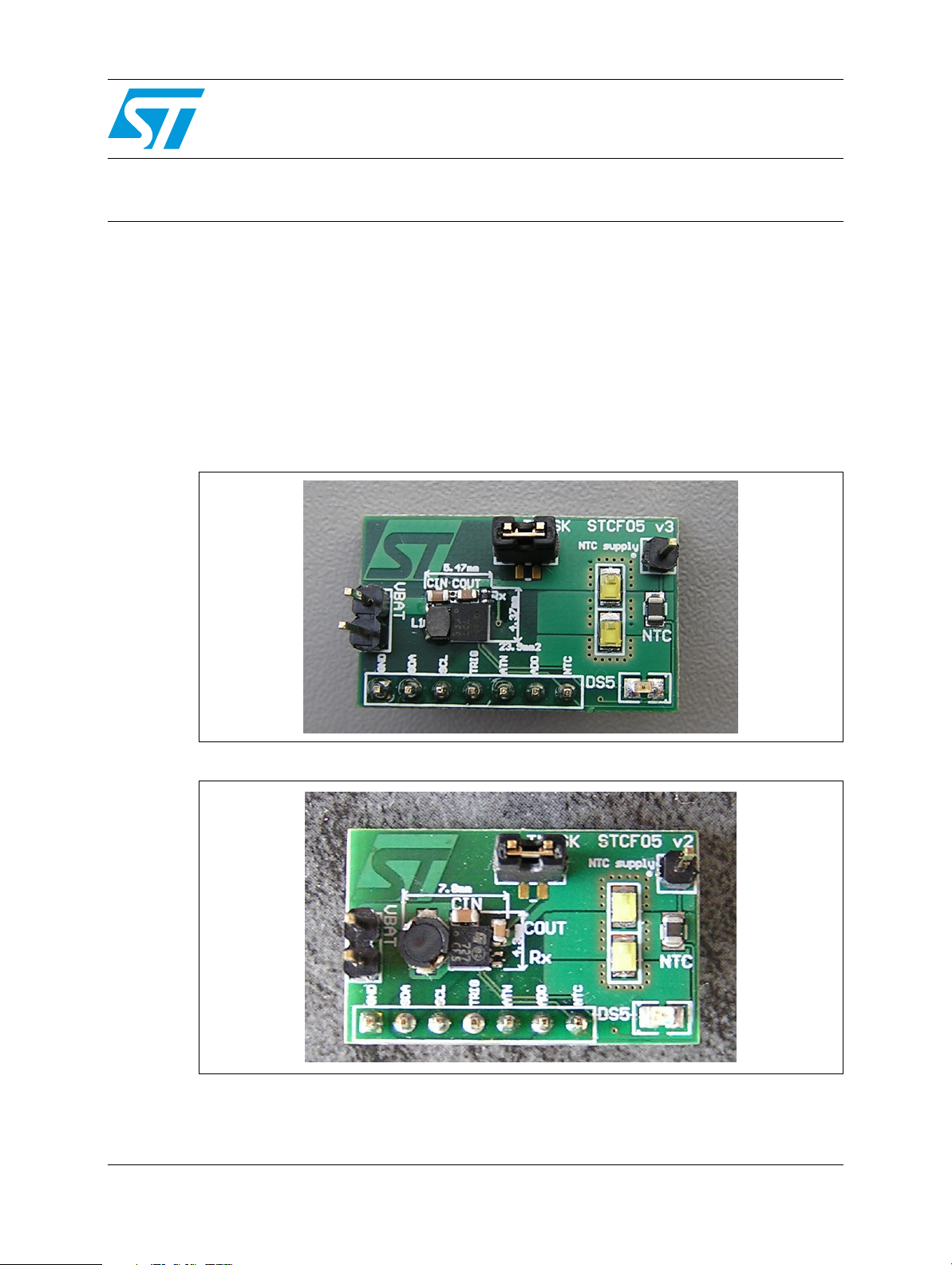
Figure 1. Demonstration board STCF05 v3: optimized for smallest PCB area
(24 mm²)
Figure 2. Demonstration board STCF05 v2: optimized for best efficiency
June 2009 Doc ID 15047 Rev 1 1/30
www.st.com
Page 2

Contents AN2827
Contents
1 Schematic description . . . . . . . . . . . . . . . . . . . . . . . . . . . . . . . . . . . . . . . 4
2 Selection of external components . . . . . . . . . . . . . . . . . . . . . . . . . . . . . . 5
2.1 Input and output capacitor selection . . . . . . . . . . . . . . . . . . . . . . . . . . . . . . 5
2.2 Inductor selection . . . . . . . . . . . . . . . . . . . . . . . . . . . . . . . . . . . . . . . . . . . . 5
2.3 LED selection . . . . . . . . . . . . . . . . . . . . . . . . . . . . . . . . . . . . . . . . . . . . . . . 5
2.4 NTC and RX resistor selection . . . . . . . . . . . . . . . . . . . . . . . . . . . . . . . . . . 5
3 PCB design . . . . . . . . . . . . . . . . . . . . . . . . . . . . . . . . . . . . . . . . . . . . . . . . 7
3.1 PCB design rules . . . . . . . . . . . . . . . . . . . . . . . . . . . . . . . . . . . . . . . . . . . . 7
3.2 PCB layout . . . . . . . . . . . . . . . . . . . . . . . . . . . . . . . . . . . . . . . . . . . . . . . . . 8
3.2.1 Four-layer PCB with 33.54 mm² application area using
VLF4014AT-1R0N2R2 coil 8
3.2.2 Four-layer PCB with 23.9 mm² application area using
VLS252012T-1R0N1R7 coil 11
4 Internal registers . . . . . . . . . . . . . . . . . . . . . . . . . . . . . . . . . . . . . . . . . . . 14
5 Operation modes . . . . . . . . . . . . . . . . . . . . . . . . . . . . . . . . . . . . . . . . . . . 15
5.1 SHUTDOWN mode . . . . . . . . . . . . . . . . . . . . . . . . . . . . . . . . . . . . . . . . . 15
5.2 SHUTDOWN mode with NTC feature activated . . . . . . . . . . . . . . . . . . . . 15
5.3 READY mode NTC . . . . . . . . . . . . . . . . . . . . . . . . . . . . . . . . . . . . . . . . . . 15
5.4 Torch mode . . . . . . . . . . . . . . . . . . . . . . . . . . . . . . . . . . . . . . . . . . . . . . . . 16
5.5 Flash mode . . . . . . . . . . . . . . . . . . . . . . . . . . . . . . . . . . . . . . . . . . . . . . . . 17
6 STATUS register and ATN pin . . . . . . . . . . . . . . . . . . . . . . . . . . . . . . . . . 19
7 Reading and writing to the STCF05 registers through the I²C bus . . . 20
7.1 Writing to a single register . . . . . . . . . . . . . . . . . . . . . . . . . . . . . . . . . . . . 20
7.2 Writing to multiple registers with incremental addressing . . . . . . . . . . . . 20
7.3 Reading from a single register . . . . . . . . . . . . . . . . . . . . . . . . . . . . . . . . . 21
7.4 Reading from multiple registers with incremental addressing . . . . . . . . . 22
8 Examples of register setup for each mode . . . . . . . . . . . . . . . . . . . . . . 23
2/30 Doc ID 15047 Rev 1
Page 3

AN2827 Contents
8.1 Example 1: 400 mA flash with 700 ms duration . . . . . . . . . . . . . . . . . . . . 23
8.2 Example 2: 15 mA torch . . . . . . . . . . . . . . . . . . . . . . . . . . . . . . . . . . . . . . 24
8.3 Example 3: auxiliary LED running at 10 mA for 500 ms . . . . . . . . . . . . . . 25
8.4 Example 4: red-eye reduction (multiple short flashes) . . . . . . . . . . . . . . . 25
8.5 Example 5: flash pulse longer than 1.5 s . . . . . . . . . . . . . . . . . . . . . . . . . 27
9 Revision history . . . . . . . . . . . . . . . . . . . . . . . . . . . . . . . . . . . . . . . . . . . 29
Doc ID 15047 Rev 1 3/30
Page 4
Schematic description AN2827
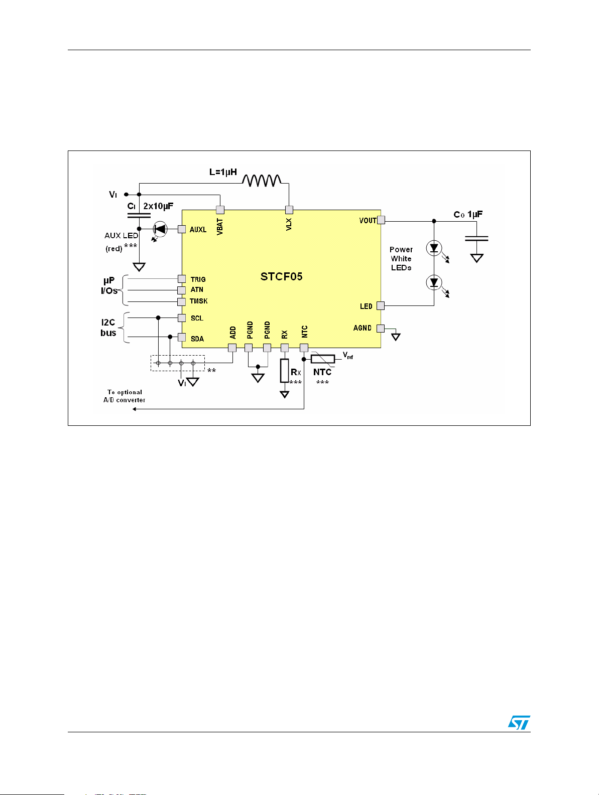
1 Schematic description
The STCF05 flash LED driver has a high operational frequency (1.8 MHz) which allows the
use of small-sized external components.
Figure 3. Typical application schematic
**: Connect to VI, GND, SDA or SCL to choose one of the four different I²C slave addresses.
***: Optional components to support auxiliary functions.
4/30 Doc ID 15047 Rev 1
Page 5

AN2827 Selection of external components
2 Selection of external components
2.1 Input and output capacitor selection
It is recommended to use ceramic capacitors with low ESR as input and output capacitors. It
is also recommended to use 10 µF/6.3 V as a minimum value for the input capacitor, and
1 µF/16 V as the optimal value for the output capacitor to achieve a good stability of the
device, for a supply range varying from a low input voltage (2.5 V) to the maximum ratings of
output power.
Note: See recommended components in Ta bl e 1 .
2.2 Inductor selection
A thin shielded inductor with a low DC series resistance of winding is recommended for this
application. To achieve a good efficiency in step-up mode, we recommend using an inductor
with a DC series resistance R
the LED [Ω; Ω, 1].
For nominal operation, the peak inductor current can be calculated by the formula:
= RD / 10 [Ω; Ω, 1], where RD is the dynamic resistance of
DCL
I
PEAK
= [(I
OUT
/ η) + (V
- VIN) x V
OUT
) / (2 x L x F x V
IN²
Where:
I
Peak inductor current
PEAK
I
Current sourced at the V
OUT
OUT
-pin
η Efficiency of the STCF05
V
Output voltage at the V
OUT
V
Input voltage at the V
IN
BAT
OUT
-pin
-pin
L Inductance value of the inductor
F Switching frequency
Note: See recommended components in Ta bl e 1 .
2.3 LED selection
Any string of LEDs with a cumulative forward voltage ranging from 5.3 to 10.2 V is
compatible with the STCF05. The total LED spread must be taken into account when
calculating the minimum and maximum voltage of the LEDs that must be inside the
5.3 –10.2 voltage range. It is possible to set the level of the LED current to flash mode and
torch mode by setting the corresponding registers through the I²C interface.
Note: See recommended components in Ta bl e 1 .
OUT²
)] x V
OUT
/ V
IN
2.4 NTC and RX resistor selection
Optionally, the STCF05 uses a negative thermistor (NTC) to sense the LED temperature, as
well as an R
resistor and an external voltage reference in order to use the NTC feature.
X
Refer to Figure 3: Typical application schematic for more details.
Doc ID 15047 Rev 1 5/30
Page 6

Selection of external components AN2827
Once the NTC feature is activated through the I²C, the internal switch connects the RX
resistor to the NTC; this creates a voltage divider supplied by the external reference voltage
connected to the NTC.
If the temperature of the NTC thermistor rises as a result of the heat dissipated by the LED,
the voltage on the NTC pin increases. When this voltage exceeds 0.56 V, the NTC_W bit in
the STATUS register is set to High, and the ATN pin is set to Low to inform the
microcontroller that the LED is becoming hot. The NTC_W bit is cleared by reading the
STATUS register.
If the voltage on the NTC pin rises further and exceeds 1.2 V, the NTC_H bit in the STATUS
register is set to High, and the ATN pin is set to Low to inform the microcontroller that the
LED is too hot, and the device switches automatically to READY mode to avoid damaging
the LED. This status is latched until the microcontroller reads the STATUS register. Reading
the STATUS register clears the NTC_H bit.
The selection of the NTC and R
resistor values strongly depends on the power dissipated
X
by the LED and all the components surrounding the NTC thermistor, and on the cooling
capabilities of each specific application. The R
and NTC values in Tab le 1 work well for the
X
demonstration board presented in this application note. A real-life application may require a
different type of NTC thermistor to achieve optimal thermal protection.
The procedure to activate the NTC feature is described in Section 5.2: SHUTDOWN mode
with NTC feature activated.
Table 1. List of components
Component Manufacturer Part number Value Size
1. Used in v2 version to achieve best efficiency.
2. Used in v3 version, when low application area down to 23.9 mm² is preferred.
C
I
C
O
LTDK
TDK C1608X5R0J106M 10 µF 0603
TDK C1608X5R1A105M 1 µF 0603
VLF4014AT-1R0N2R2
VLS252012T-1R0N1R7
(1)
(2)
1 µH 3.7 x 3.5 x 1.2 mm
1 µH 2.5 x 2 x 1.2 mm
NTC Murata NCP21WF104J03RA 100 kΩ 0805
R
X
Rohm MCR01MZPJ15K 15 kΩ 0402
LED Luxeon LED 2x LXCL-PWF1 0805
AUXLED Rohm SML-210VT 0805
6/30 Doc ID 15047 Rev 1
Page 7

AN2827 PCB design
3 PCB design
3.1 PCB design rules
The STCF05 is a powerful switching device that operates with low input voltages and a high
duty cycle. The PCB must be designed in line with switched mode power supply design
rules. The power tracks (or wires on the demonstration board) must be as short as possible
and wide enough, because of the large currents involved. It is recommended to use a
4-layer PCB to get the best performance. All external components must be placed as close
as possible to STCF05. All high-energy switched loops should be as small as possible to
reduce EMI.
Most of the LEDs need to be cooled efficiently. This can be achieved by using a dedicated
copper area on the PCB. Refer to the selected LED's reference guide to design the proper
heatsink. In case a modification of any PCB layer should be required, it is highly
recommended to use enough vias. Place the NTC resistor as close as possible to the LED
for good temperature sensing. A direct connection between GND and PGND is necessary to
achieve a correct output current value. No LED current should flow through this track. Vias
connecting the STCF05 pins to the copper tracks (if used) must be 0.1 mm in diameter. It is
recommended to use the filled vias.
It is possible to route the STCF05 device with a total PCB area of 23.9 mm² using the TDK
inductor VLS252012 1 µH value. When using the VLF4014AT, the application area is
increased by 9.6 mm², and the efficiency of the application is improved up to 85%.
Doc ID 15047 Rev 1 7/30
Page 8
PCB design AN2827
3.2 PCB layout
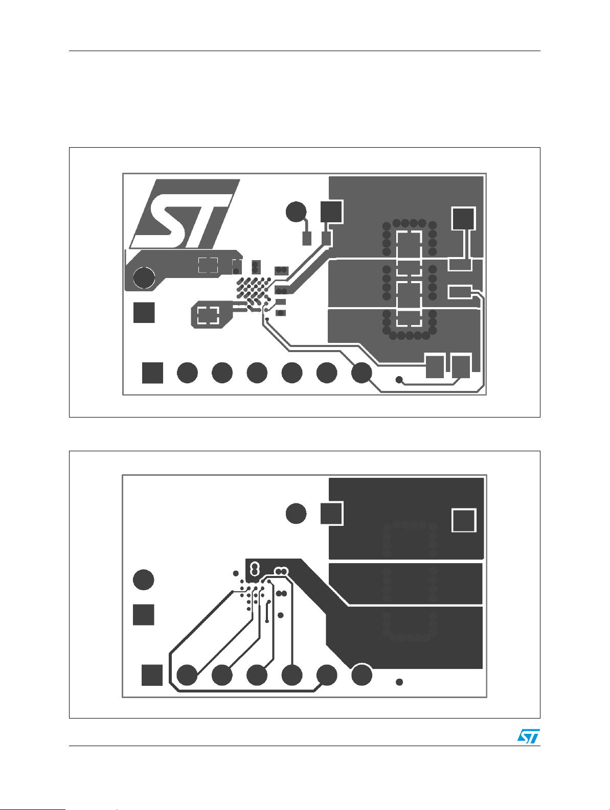
3.2.1 Four-layer PCB with 33.54 mm² application area using
VLF4014AT-1R0N2R2 coil
Figure 4. Top layer
Figure 5. Middle layer 1
8/30 Doc ID 15047 Rev 1
Page 9
AN2827 PCB design
Figure 6. Middle layer 2
Figure 7. Bottom layer
Doc ID 15047 Rev 1 9/30
Page 10

PCB design AN2827
Figure 8. Top overlay
10/30 Doc ID 15047 Rev 1
Page 11

AN2827 PCB design
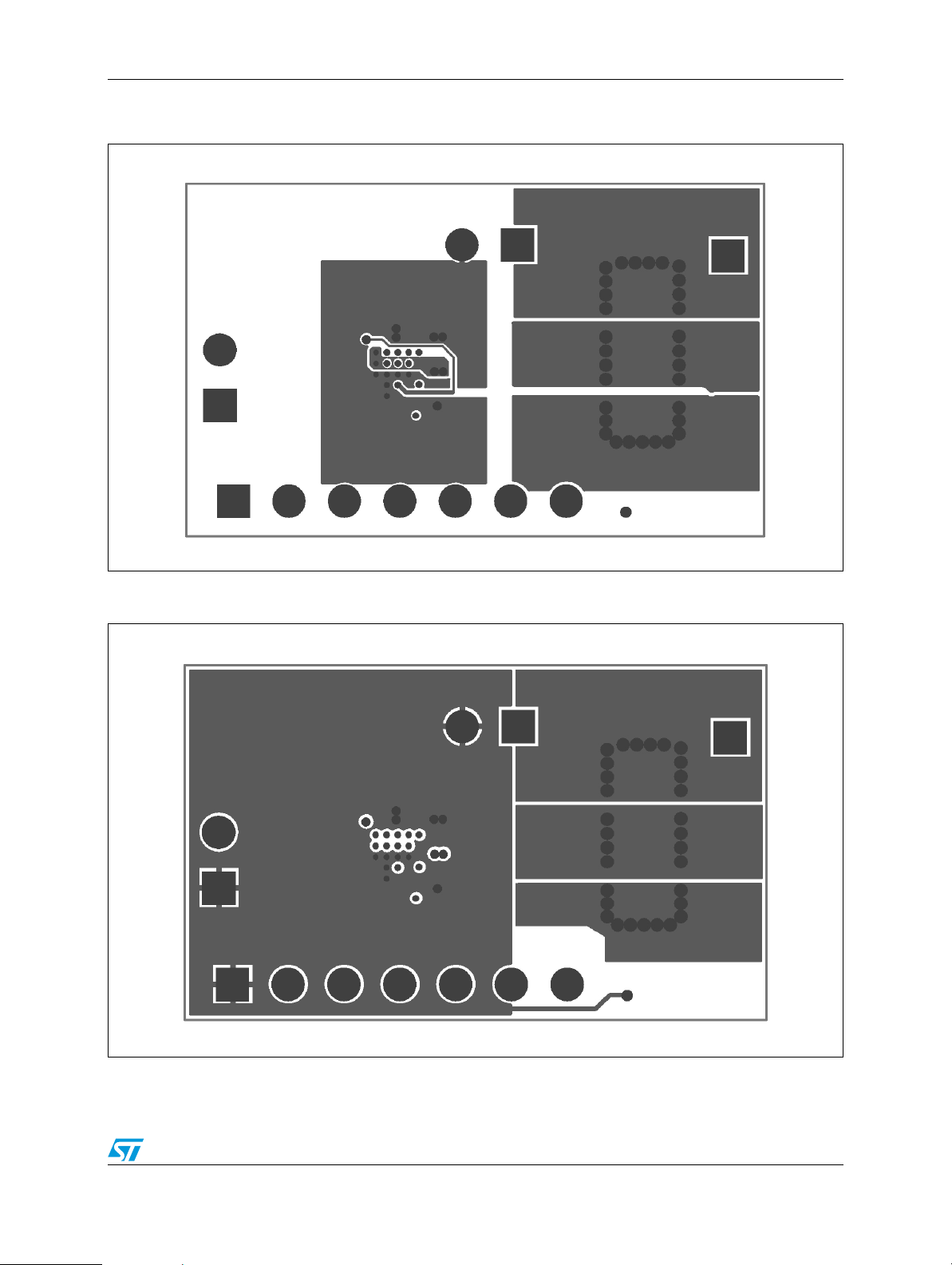
3.2.2 Four-layer PCB with 23.9 mm² application area using
VLS252012T-1R0N1R7 coil
Figure 9. Top layer
Figure 10. Middle layer 1
Doc ID 15047 Rev 1 11/30
Page 12

PCB design AN2827
Figure 11. Middle layer 2
Figure 12. Bottom layer
12/30 Doc ID 15047 Rev 1
Page 13

AN2827 PCB design
Figure 13. Top overlay
Doc ID 15047 Rev 1 13/30
Page 14

Internal registers AN2827
4 Internal registers
The STCF05 has four internal registers: COMMAND, DIMMING, AUX_LED and STATUS.
The STATUS register is read-only.
The COMMAND register can be accessed in any operating mode. All the other registers can
be accessed in any mode, except in SHUTDOWN mode. When the device enters
SHUTDOWN mode, the DIMMING, AUX_LED and STATUS registers are cleared. The
COMMAND register value remains untouched when entering SHUTDOWN mode.
Ta bl e 2 shows the accessibility of each register in all operation modes.
Table 2. Accessibility of internal registers
Mode
Register Address
Shutdown Ready Torch Flash
Shutdown
value
Power-ON
reset value
COMMAND 00 Read/Write Read/Write Read/Write Read/Write Untouched Cleared
DIMMING 01 Inaccessible Read/Write Read/Write Read/Write Cleared Cleared
AUX_LED 02 Inaccessible Read/Write Read/Write Read/Write Cleared Cleared
STATUS 03 Inaccessible Read-only Read-only Read-only Cleared Cleared
14/30 Doc ID 15047 Rev 1
Page 15

AN2827 Operation modes
5 Operation modes
5.1 SHUTDOWN mode
SHUTDOWN mode is entered after a power-ON reset. This mode is mainly used to
decrease the power consumption of the device. During this mode, only the I²C interface is
active. The only thing which can be done in SHUTDOWN mode is to access the COMMAND
register. Entering SHUTDOWN mode by writing to the COMMAND register will abort any
running operation and clear the values of the DIMMING, AUX_LED and STATUS registers.
The COMMAND register value is not affected by entering SHUTDOWN mode.
The following data must be written to the COMMAND register to enter SHUTDOWN mode.
Table 3. COMMAND register data to enter SHUTDOWN mode
PWR_ON TRIG_EN TCH_ON NTC_ON FTIM_3 FTIM_2 FTIM_1 FTIM_0
CMD_REG
0xxxxxxx
MSB LSB
5.2 SHUTDOWN mode with NTC feature activated
When this operation mode is activated, the microcontroller can still monitor the NTC voltage
through its A/D converter, while the STCF05 remains in SHUTDOWN mode and therefore
saves power.
The following data must be written to the COMMAND register to enter SHUTDOWN mode
with NTC activated.
Table 4. COMMAND register data to enter SHUTDOWN mode with NTC activated
CMD_REG
PWR_ON TRIG_EN TCH_ON NTC_ON FTIM_3 FTIM_2 FTIM_1 FTIM_0
0xx1xxxx
MSB LSB
5.3 READY mode NTC
The READY mode allows the user to access all the internal registers. The NTC feature can
be activated in this mode and the temperature of the LED can be sensed by the A/D
converter of the microcontroller.
The following data must be written to the COMMAND register to enter READY mode.
Table 5. COMMAND register data to enter READY mode with NTC activated
CMD_REG
PWR_ON TRIG_EN TCH_ON NTC_ON FTIM_3 FTIM_2 FTIM_1 FTIM_0
1000xxxx
MSB LSB
Doc ID 15047 Rev 1 15/30
Page 16

Operation modes AN2827
Table 6. COMMAND register data to enter READY mode
PWR_ON TRIG_EN TCH_ON NTC_ON FTIM_3 FTIM_2 FTIM_1 FTIM_0
CMD_REG
1001xxxx
MSB LSB
As soon as the NTC feature is activated, the internal switch connects the NTC resistor to the
RX resistor, there by creating a voltage divider. The voltage on this divider can be, if desired,
monitored by the A/D converter of the microcontroller. An external voltage reference must be
connected to the NTC to use this feature. The bits NTC_W and NTC_H of the STATUS
register will not be properly set if there is no external reference voltage connected to the
NTC.
If the NTC feature is not going to be used, neither the negative thermistor nor the external
reference needs to be connected. In this case, it is recommended to ground the RX pin. As
the NTC feature is automatically activated during the flash and torch mode, leaving the RX
pin floating could lead to unwanted interruptions of the light due to non-defined voltages on
the RX pin.
5.4 Torch mode
This mode is intended to be used for low light intensities. The LED current in torch mode can
be adjusted in a range from 15 mA up to 120 mA.
The torch mode is activated by writing the following data to the COMMAND register.
Table 7. COMMAND register data to enter torch mode
CMD_REG
PWR_ON TRIG_EN TCH_ON NTC_ON FTIM_3 FTIM_2 FTIM_1 FTIM_0
101xxxxX
MSB LSB
The DIMMING register value (TDIM) must be set as well, unless it has already been set
during a previous operation. If the TDIM register is not set, then the default output current
value will be at the minimum.
As soon as the torch mode is activated, it remains active until a new mode is entered by
writing new data to the COMMAND register.
If the torch mode was terminated by entering READY or flash mode, it can be restarted by
writing the corresponding data to the COMMAND register only, because entering any of the
READY and flash modes does not influence the TDIM value. If the torch mode was
terminated by entering SHUTDOWN mode, then the TDIM value must be set again during
the restart of the torch mode because entering the SHUTDOWN mode clears the TDIM
value.
As soon as the torch mode is activated, the NTC feature is automatically activated too so as
to protect the LED from overheating. The NTC feature will be activated even if the NTC_ON
bit in the COMMAND register is set to zero.
16/30 Doc ID 15047 Rev 1
Page 17

AN2827 Operation modes
5.5 Flash mode
This mode is intended to be used for high light intensities. The LED current in flash mode
can be adjusted up to 400 mA with the input voltage ranging from 2.5 to 5.5 V.
The flash mode is activated by writing the following data to the COMMAND register.
Table 8. COMMAND register data to enter flash mode
CMD_REG
PWR_ON TRIG_EN TCH_ON NTC_ON FTIM_3 FTIM_2 FTIM_1 FTIM_0
11xxxxxx
MSB LSB
The DIMMING register value (FDIM) must be written in order to set the desired flash current,
while the FTIM_0 ~ 3 are used to set a maximum time duration for the flash. Values from
0 ~15 correspond to 0 ~1.5 s (100 ms steps). This allows a better safety of the system
providing a certain turn-off of the flash even in case of application software problems.
The activation of the flash mode requires the TRIG pin to be High. The flash mode is active
only when the TRIG_EN bit in the COMMAND register is set to 1 and the TRIG pin is High.
This gives the user the possibility to choose between a soft and a hard triggering of the flash
mode.
The soft triggering is done by writing data to the internal registers only, while the TRIG pin is
permanently kept High, for example by connecting it to V
. This saves one pin of the
BAT
microcontroller, which can be used for a different purpose, but this way of triggering is less
accurate than the hard one. The second disadvantage of this solution is that the flash
duration can only be set in discrete steps of the internal timer (1 step = approx. 100 ms).
Hard triggering of the flash mode requires the microcontroller to manage the TRIG pin. The
COMMAND and DIMMING registers are loaded with data before the TRIG pin is set to High.
This allows the user to avoid the I²C bus latency. The flash mode then starts as soon as the
TRIG pin is set to High. It takes typically about 0.7 ms to ramp-up the LED current to the
adjusted value. This time may vary according to the LED current value and the battery
voltage.
If the TRIG pin is kept High for more than the FTIM value, the internal timer reaches zero
and the flash mode is terminated. As soon as the flash is timed out, the ATN pin is pulled
down for 11 µs to inform the microcontroller that the STATUS register has been updated and
that the flash is over. If the TRIG pin is set to Low before the internal timer reaches zero, the
flash mode will be interrupted and can be restarted by setting the TRIG pin High again. The
internal timer is stopped while the TRIG pin is Low. This means that the user can split the
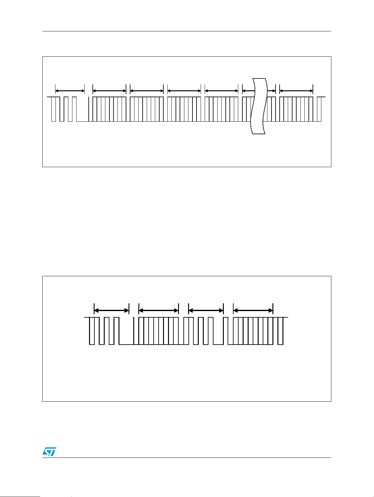
flash into several pulses of a total length equal to the FTIM value. Figure 14 shows the
splitting of the flash into several shorter pulses. The cumulative length of all the pulses is
determined by the FTIM value. Figure 14 shows the case for
FTIM = 9 (900 ms flash time). The cumulative time when the TRIG pin is High is 1000 ms (5
pulses 200 ms long). The last flash pulse will be100 ms long only. The reason is that the
internal flash timer reaches zero and the TRIG_EN bit is set to 0.
Doc ID 15047 Rev 1 17/30
Page 18

Operation modes AN2827
Figure 14. Splitting the flash pulse into several shorter pulses
1300 ms
200
200
ms
ms
98765 4321 0
98765 4321 0
100
100
ms
ms
1300 ms
Time when the
Time when the
internal flash
internal flash
timer reaches 0
timer reaches 0
I²C bus packet
I²C bus packet
TRIG_EN bit
TRIG_EN bit
TRIG pin
TRIG pin
LED current
LED current
Internal Flash timer values
Internal Flash timer values
Hard triggering therefore allows a smooth setting of the flash duration. The resolution is
about 8.8 µs. The minimum flash duration is limited by the ramp-up time of the LED current
and the maximum is limited by the FTIM value. If it is necessary to make a flash pulse longer
then the maximum allowed by FTIM, then it is necessary to reload the COMMAND register
before the internal timer reaches zero (start a new flash before the previous one elapses).
See Section 8.5: Example 5: flash pulse longer than 1.5 s for more details.
18/30 Doc ID 15047 Rev 1
Page 19

AN2827 STATUS register and ATN pin
6 STATUS register and ATN pin
Table 9. STATUS register bits
Bit name LED_S F_RUN LED_F NTC_W NTC_H OT_F OC_F VOUTOK_N
MSB LSB
Refer to the STCF05 datasheet for a detailed description of each bit.
Table 10. Effect of the STATUS register bits on the operation of the device
Bit Name LED_S
Default
value
Latched
Forces
READY
mode
when set
Sets ATN
LOW when
set
F_RUN
STAT_REG
LED_O
STAT_REG
NTC_W
STAT_REG
NTC_H
STAT_REG
OT_F
STAT_REG
OC_F
STAT_REG
VOUTOK_N
STAT_REG
0000000 0
(1)
YES NO YES YES YES YES No YES
NO NO YES NO YES YES NO YES
YES NO YES YES YES YES NO YES
1. YES means that the bit is set by internal signals and is reset to its default value by an I²C read operation of STAT_REG.
NO means that the bit is set and reset by internal signals in real-time.
When the status register is latched, reading and writing to the registers is still possible, but
the bits TRIG_EN and TCH_ON in the COMMAND register and AUXL register cannot be
changed until the device is unlatched. It is necessary to read the STATUS register to unlatch
the device.
The ATN pin is also pulled down when the internal timer reaches zero in flash mode. In this
case, the ATN pin is pulled down for 11 µs only. It is recommended to connect the ATN pin to
the interrupt input of the microcontroller. If it is not connected to the interrupt input, the ATN
pin should be polled fast enough not to miss the 11 µs pulse; for example, by a programming
loop which is entered after the start of flash mode. This loop will run until the ATN pin goes
Low. It is recommended to make a timeout of such a loop.
Doc ID 15047 Rev 1 19/30
Page 20

Reading and writing to the STCF05 registers through the I²C bus AN2827
7 Reading and writing to the STCF05 registers through
the I²C bus
7.1 Writing to a single register
Writing to a single register starts with a START bit followed by the 7-bit device address of the
STCF05. The 8
th
bit is the R/W bit, which is 0 in this case. R/W = 1 means a reading
operation. The master then waits for an acknowledgement from the STCF05. The 8-bit
address of the desired register is sent afterwards to the STCF05. It is also followed by an
acknowledge pulse. The last transmitted byte is the data that is going to be written into the
register. It is followed again by an acknowledge pulse from the STCF05. The master then
generates a STOP bit and the communication is over. The whole cycle is represented in
Figure 15.
Figure 15. Writing to a single register
W
W
DEVICE
DEVICE
DEVICE
ADDRESS
ADDRESS
ADDRESS
7 bits
7 bits
7 bits
M
M
M
S
S
S
S
S
S
T
T
T
B
B
B
A
A
A
R
R
R
T
T
T
W
R
R
R
I
I
I
T
T
T
E
E
E
A
A
A
L
L
L
R
R
R
C
C
C
S
S
S
/
/
/
K
K
K
B
B
B
W
W
W
M
M
M
S
S
S
B
B
B
SDA LINE
SDA LINE
ADDRESS OF
ADDRESS OF
ADDRESS OF
REGISTER
REGISTER
REGISTER
DATA
DATA
DATA
A
A
A
A
M
A
M
A
M
L
L
L
C
C
C
C
S
C
S
C
S
S
S
S
K
K
K
K
B
K
B
K
B
B
B
B
A
A
A
S
S
S
L
L
L
C
C
C
T
T
T
S
S
S
K
K
K
O
O
O
B
B
B
P
P
P
7.2 Writing to multiple registers with incremental addressing
It would be unpractical to send several times the device address and the address of the
register when writing to multiple registers. The STCF05 supports writing to multiple registers
with incremental addressing. When data is written to a register, the register address is
automatically incremented (by one), and therefore the next data can be sent without
resending the device address and the register address (see Figure 16).
20/30 Doc ID 15047 Rev 1
Page 21
AN2827 Reading and writing to the STCF05 registers through the I²C bus
Figure 16. Writing to multiple register
W
W
7 bits
7 bits
7 bits
W
R
R
R
ADDRESS OF
ADDRESS OF
ADDRESS OF
I
I
I
REGISTER i
REGISTER i
REGISTER i
T
T
T
E
E
E
DATA i
DATA i
DATA i
DATA i+1
DATA i+1
DATA i+1
DATA i+2
DATA i+2
DATA i+2
DATA i+2
DATA i+2
DATA i+2
DATA i+n
DATA i+n
DATA i+n
DEVICE
DEVICE
DEVICE
ADDRESS
ADDRESS
ADDRESS
A
A
A
A
S
S
S
M
M
M
T
T
T
S
S
S
A
A
A
B
B
B
R
R
R
T
T
T
A
R
R
R
M
M
M
L
L
L
C
C
C
/
/
/
S
S
S
S
S
S
K
K
K
W
W
W
B
B
B
B
B
B
A
A
M
A
M
A
M
M
M
M
L
L
L
C
C
C
C
S
C
S
C
S
S
S
S
S
S
S
K
K
K
K
B
K
B
K
B
B
B
B
B
B
B
A
A
A
M
M
M
L
L
L
C
C
C
S
S
S
S
S
S
K
K
K
B
B
B
B
B
B
SDA LINE
SDA LINE
L
L
L
S
S
S
B
B
B
7.3 Reading from a single register
The reading operation starts with a START bit followed by the 7-bit device address of the
STCF05. The 8
receiving of the address + R/W bit by an acknowledge pulse. The address of the register
which should be read is then sent and confirmed by another acknowledge pulse from the
STCF05. The master then generates another START bit and sends the device address
followed by the R/W-bit, which is now 1. The STCF05 confirms the receiving of the address
+ R/W-bit by an acknowledge pulse, and starts to send data to the master. No acknowledge
pulse from the master is required after receiving the data. The master then generates a
STOP bit to terminate the communication.
Figure 17. Reading from a single register
DEVICE
DEVICE
ADDRESS
ADDRESS
7 bits
7 bits
th
bit is the R/W bit, which is 0 in this case. The STCF05 confirms the
W
W
R
R
I
I
T
T
E
E
ADDRESS
ADDRESS
OF
OF
REGISTER
REGISTER
DEVICE
DEVICE
ADDRESS
ADDRESS
A
A
A
M
M
M
C
C
C
S
S
S
K
K
K
B
B
B
7 bits
7 bits
A
A
A
L
L
L
M
M
M
C
C
C
S
S
S
S
S
S
K
K
K
B
B
B
B
B
B
R
R
E
E
A
A
D
D
DATA
DATA
L
L
L
M
M
M
A
A
A
S
S
S
S
S
S
C
C
C
B
B
B
B
B
B
K
K
K
A
A
A
S
S
S
L
L
L
C
C
C
T
T
T
S
S
S
K
K
K
O
O
O
B
B
B
P
P
P
M
M
S
S
S
S
T
T
B
B
A
A
R
R
T
T
L
L
A
M
A
M
R
R
S
S
C
S
C
S
/
/
B
B
K
B
K
B
W
W
A
L
A
L
S
S
C
S
C
S
T
T
K
B
K
B
A
A
R
R
T
T
SDA LINE
SDA LINE
L
A
R
A
R
C
/
C
/
K
W
K
W
L
S
N
S
N
S
S
T
O
T
O
B
B
O
O
P
P
A
A
C
C
K
K
Doc ID 15047 Rev 1 21/30
Page 22
Reading and writing to the STCF05 registers through the I²C bus AN2827
7.4 Reading from multiple registers with incremental addressing
Reading from multiple registers starts in the same way as reading from a single register. As
soon as the first register is read, the register address is automatically incremented. If the
master generates an acknowledge pulse after receiving the data from the first register, then
reading from the next register can start immediately without having to resend the device and
register addresses. The last acknowledge pulse before the STOP bit is not required.
Figure 18. Reading from multiple registers
W
W
DEVICE
DEVICE
ADDRESS
ADDRESS
7 bits
7 bits
R
R
T
T
E
E
I
I
ADDRESS OF
ADDRESS OF
REGISTER i
REGISTER i
DEVICE
DEVICE
ADDRESS
ADDRESS
7 bits
7 bits
R
R
E
E
DATA i
DATA i
A
A
D
D
DATA i+1
DATA i+1
DATA i+2
DATA i+2
DATA i+2
DATA i+2
DATA i+n
DATA i+n
M
S
S
M
M
T
T
S
S
A
A
B
B
R
R
T
T
M
R
R
A
A
L
L
S
S
/
/
C
C
S
S
B
B
W
W
K
K
B
B
A
L
A
L
S
S
C
S
C
S
T
T
K
B
K
B
A
A
R
R
T
T
A
R
A
R
C
/
C
/
K
W
K
W
L
L
S
S
B
B
SDA LINE
SDA LINE
A
A
M
M
C
C
S
S
K
K
B
B
A
L
A
L
M
M
C
S
C
S
S
S
K
B
K
B
B
B
A
L
A
L
M
M
C
S
C
S
S
S
K
B
K
B
B
B
L
L
M
A
M
A
S
S
S
C
S
C
B
B
B
K
B
K
S
S
L
N
L
N
T
T
S
O
S
O
O
O
B
B
P
P
A
A
C
C
K
K
22/30 Doc ID 15047 Rev 1
Page 23

AN2827 Examples of register setup for each mode
8 Examples of register setup for each mode
Table 11. Torch and flash mode dimming register settings
LDIM (hex) 0 1 2 3 4 5 6 7 8 9 A B C
TDIM (hex)
FDIM(hex)
LED current [mA] 15 20 30 45 60 75 90 120 160 200 240 320 400
Internal step 12345678910111213
8.1 Example 1: 400 mA flash with 700 ms duration
The value of FDIM (4 bits) must be set to 0x7 to set-up the current source to the chosen
value (Ta bl e 1 1 ).
The flash duration timer can be set from 100 ms up to 1500 ms in 100 ms steps. If the
desired flash duration is 700 ms the FTIM value (4 bits) must be se to 0x7.
The PWR_ON bit of the command register must be set to 1.
0 1 2 3 4 5 6 7
0 1 2 3 4 5 6 7
The TRIG_EN bit of the command register must be set to 1.
The TCH_ON bit of the command register must be set to 0.
The NTC_ON bit of the command register can be set to any value because NTC is
automatically ON when the flash mode is active. Setting this bit to 0 will not switch off the
NTC.
Table 12. COMMAND register data to enter flash mode
CMD_REG PWR_ON TRIG_EN TCH_ON NTC_ON FTIM_3 FTIM_2 FTIM_1 FTIM_0
Table 13. DIMMING register data for flash mode
DIM_REG N/A TDIM_2 TDIM_1 TDIM_0 N/A FDIM_2 FDIM_1 FDIM_0
11xX0111
MSB LSB
00000111
MSB LSB
Four bytes must be written to the STCF05 to make a flash.
Table 14. I²C data packet for activating flash mode
Byte Hex Binary Comment
1 62 01100010Device address + R/W bit
2 00 00000000Command register address
3 D7 11010111Data of the command register
4 07 00000111Data of the dimming register
Doc ID 15047 Rev 1 23/30
Page 24

Examples of register setup for each mode AN2827
8.2 Example 2: 15 mA torch
The value of TDIM (4 bits) must be set to 0x0 to set-up the current source to the chosen
value.
The PWR_ON bit of the command register must be set to 1.
The TRIG_EN bit of the command register must be set to 1.
The TCH_ON bit of the command register must be set to 0.
The NTC_ON bit of the command register can be set to any value because NTC is
automatically ON when the torch mode is active. Setting this bit to 0 will not switch off the
NTC.
Table 15. COMMAND register data for torch mode
CMD_REG PWR_ON TRIG_EN TCH_ON NTC_ON FTIM_3 FTIM_2 FTIM_1 FTIM_0
10110000
MSB LSB
Table 16. DIMMING register data for torch mode
DIM_REG N/A TDIM_2 TDIM_1 TDIM_0 N/A FDIM_2 FDIM_1 FDIM_0
00000000
MSB LSB
Four bytes must be written to the STCF05 to run the torch mode.
Table 17. I²C data packet to activate torch mode
Byte Hex Binary Comment
1 62 01100010Device address + R/W bit
2 00 00000000Command register address
3 B0 10110000Data of the command register
4 00 00000000Data of the dimming register
The duration of the torch mode is "unlimited". Torch mode is terminated by setting the
TCH_ON bit in the COMMAND register to 0.
Termination of the torch mode can be done by writing the following data to the STCF05.
Table 18. I²C data packet for terminating torch mode
Byte Hex Binary Comment
1 62 01100010Device address + R/W bit
2 00 00000000Command register address
3 80 10000000Data of the command register
Terminating torch mode puts the STCF05 into READY mode.
24/30 Doc ID 15047 Rev 1
Page 25

AN2827 Examples of register setup for each mode
8.3 Example 3: auxiliary LED running at 10 mA for 500 ms
The STCF05 must be in READY mode (both TRIG_EN and TCH_ON set to 0) to activate
the auxiliary LED.
A 10 mA output current will be reached when AUXI is set to 0x8.
AUXT must be set to 0x5 to obtain a 500 ms duration of the auxiliary LED lighting.
Table 19. COMMAND register data for AUX_LED
CMD_REG PWR_ON TRIG_EN TCH_ON NTC_ON FTIM_3 FTIM_2 FTIM_1 FTIM_0
10000000
MSB LSB
Table 20. AUX_LED register data
AUX_LED AUXI_3 AUXI_2 AUXI_1 AUXI_0 AUXT_3 AUXT_2 AUXT_1 AUXT_0
10000101
MSB LSB
Writing the following three bytes to the STCF05 puts the device into READY mode. This can
be skipped if READY mode is already activated.
Table 21. I²C data packet for activating READY mode
Byte Hex Binary Comment
1 62 01100010 Device address + R/W bit
2 00 00000000 Command register address
3 80 10000000 Data of the command register
Writing the following three bytes to the STCF05 activates the auxiliary LED for the desired
time.
Table 22. I²C data packet for activating AUX_LED
Byte Hex Binary Comment
1 62 01100010 Device address + R/W bit
2 02 00000010 Auxiliary LED register address
3 85 10000101 Data of the Auxiliary LED register
8.4 Example 4: red-eye reduction (multiple short flashes)
There are two ways of reducing red eye. The first one is to use hardware triggering of the
flashes through the TRIG pin. This is the most suitable and recommended solution, as it
reduces the usage of the I²C bus and the length of each flash pulse can be adjusted
continuously. The second solution is to use the software triggering feature, which means a
periodical reloading of the COMMAND register. This will however increase traffic on the I²C
bus and the flashes can only have a set length, adjustable in 100 ms steps only.
Doc ID 15047 Rev 1 25/30
Page 26

Examples of register setup for each mode AN2827
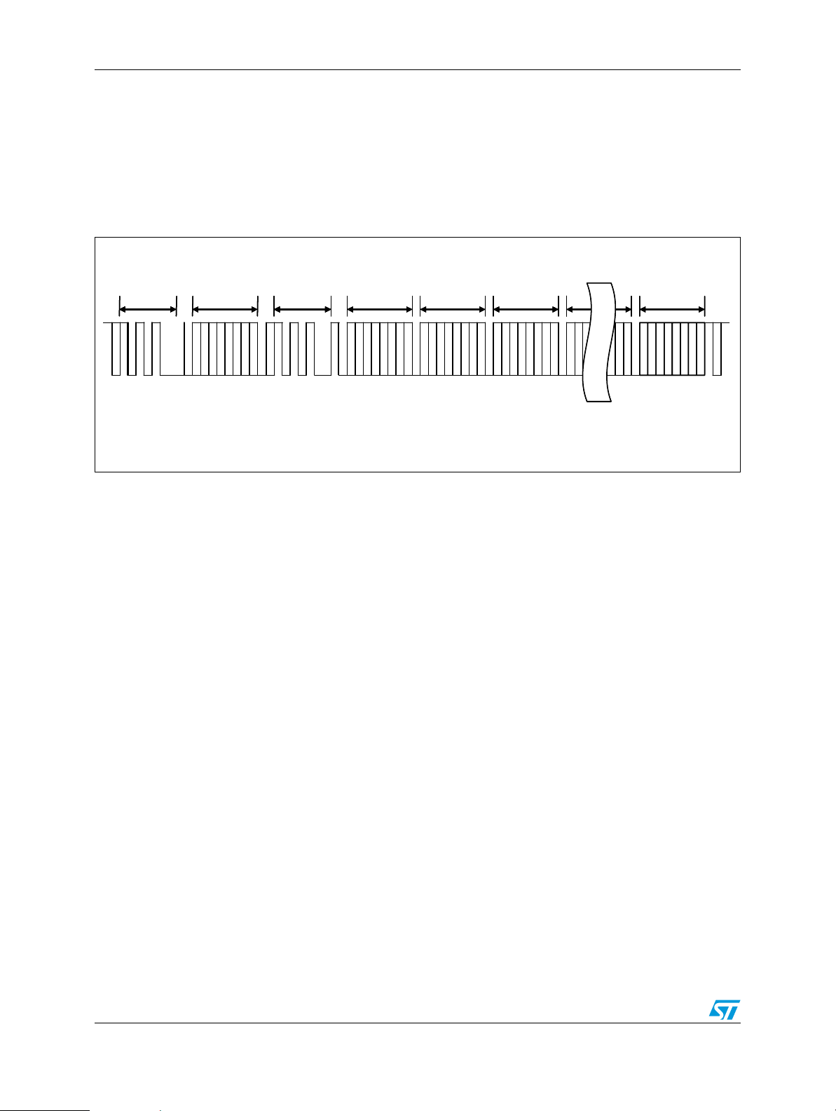
Suppose the targeted value of the flash current is 400 mA. The task is to make five flashes
of 200 ms each with a pause of 100 ms between each one.
The setting of the reference voltage is identical to the one in Example 1.
The flash timer (FTIM) will be set to 0xF, which represents 1.5 s.
Table 23. COMMAND register data for flash mode
CMD_REG PWR_ON TRIG_EN TCH_ON NTC_ON FTIM_3 FTIM_2 FTIM_1 FTIM_0
11011111
MSB LSB
Table 24. DIMMING register data for flash mode
DIM_REG N/A TDIM_2 TDIM_1 TDIM_0 N/A FDIM_2 FDIM_1 FDIM_0
00000111
MSB LSB
Ta bl e 2 5 shows the data packet to be sent.
Table 25. I²C data packet for activating flash mode
Byte Hex Binary Comment
1 62 01100010 Device address + R/W bit
2 00 00000000 Command register address
3 DF 11011111 Data of the command register
4 07 00000111 Data of the dimming register
Figure 19 shows the TRIG pin and the I²C bus timings.
Figure 19. Multiple flashes handled by TRIG pin
200
200
ms
ms
100
100
ms
ms
1400 ms
1400 ms
26/30 Doc ID 15047 Rev 1
I²C bus packet
I²C bus packet
TRIG_EN bit
TRIG_EN bit
TRIG pin
TRIG pin
Page 27

AN2827 Examples of register setup for each mode
8.5 Example 5: flash pulse longer than 1.5 s
Suppose the targeted value of the flash current is 240 mA. The task is to make a single flash
pulse with a 4-second duration.
FTIM must be reloaded into the COMMAND REGISTER before the internal flash timer
reaches zero. This guarantees that the flash will continue and not stop after 1.5 seconds.
The first packet must also contain the DIMMING REGISTER data if this data is different from
that which was used in the previous operation.
Packet 1
Sets flash mode with a 1.5 s duration and the proper dimming.
Table 26. I²C data packet for activating flash mode
Byte Hex Binary Comment
1 62 01100010 Device address + R/W bit
2 00 00000000 Command register address
3 DF 11011111 Data of the command register
4 05 00000101 Data of the dimming register
Packet 2
Sets flash mode with a 1.5 s duration. Dimming data is not reset since it is the same as for
Packet 1.
Table 27. 2nd I²C data packet for restart of flash mode
Byte Hex Binary Comment
1 62 01100010 Device address + R/W bit
2 00 00000000 Command register address
3 DF 11011111 Data of the command register
Packet 3
Sets flash mode with a 1.5 s duration. Dimming remains the same.
Table 28. 3rd I²C data packet for restart of flash mode
Byte Hex Binary Comment
1 62 01100010 Device address + R/W bit
2 00 00000000 Command register address
3 DF 11011111 Data of the command register
Packet 4
Sets flash mode with a 1 s duration. Dimming remains the same.
Doc ID 15047 Rev 1 27/30
Page 28

Examples of register setup for each mode AN2827
Table 29. 4
th
I²C data packet to restart flash mode
Byte Hex Binary Comment
1 62 01100010 Device address + R/W bit
2 00 00000000 Command register address
3 DA 11011010 Data of the command register
Figure 20 provides more details on the timing of the I²C bus packets.
The solution described in Example 5 uses a software termination of the flash pulse (it is
timed out by the internal timer.) The flash pulse could also be terminated by setting the
TRIG pin to low after 4 seconds. In this case, the fourth packet could be the same as
packets 2 and 3, because the timing of the flash is done by the TRIG pin and it is not
necessary to change the value of FTIM in the COMMAND REGISTER.
This method of periodical reloading of the COMMAND REGISTER can be used to achieve a
continuous flash light. However, it is highly recommended to guarantee an efficient cooling
of both the LED and the chip, otherwise the light can be interrupted by activation of the
thermal protections.
Figure 20. Timing of I²C bus packets for a flash lasting longer than FTIM max
Timeout of
Timeout of
the first flash
the first flash
1.5s
1.5s
1.0s 1.0s1.0s 1.0s
1.0s 1.0s1.0s 1.0s
Timeout of
Timeout of
the second
the second
flash
flash
1.5s
1.5s
4.0s
4.0s
Timeout of
Timeout of
the third flash
the third flash
1.5s
1.5s
1.0s
1.0s
Timeout of the
Timeout of the
fourth flash –
fourth flash –
ending of the
ending of the
whole flash
whole flash
pulse
pulse
I²C bus packets
I²C bus packets
TRIG_EN bit
TRIG_EN bit
TRIG pin
TRIG pin
28/30 Doc ID 15047 Rev 1
Page 29

AN2827 Revision history
9 Revision history
Table 30. Document revision history
Date Revision Changes
10-Jun-2009 1 Initial release.
Doc ID 15047 Rev 1 29/30
Page 30

AN2827
Please Read Carefully:
Information in this document is provided solely in connection with ST products. STMicroelectronics NV and its subsidiaries (“ST”) reserve the
right to make changes, corrections, modifications or improvements, to this document, and the products and services described herein at any
time, without notice.
All ST products are sold pursuant to ST’s terms and conditions of sale.
Purchasers are solely responsible for the choice, selection and use of the ST products and services described herein, and ST assumes no
liability whatsoever relating to the choice, selection or use of the ST products and services described herein.
No license, express or implied, by estoppel or otherwise, to any intellectual property rights is granted under this document. If any part of this
document refers to any third party products or services it shall not be deemed a license grant by ST for the use of such third party products
or services, or any intellectual property contained therein or considered as a warranty covering the use in any manner whatsoever of such
third party products or services or any intellectual property contained therein.
UNLESS OTHERWISE SET FORTH IN ST’S TERMS AND CONDITIONS OF SALE ST DISCLAIMS ANY EXPRESS OR IMPLIED
WARRANTY WITH RESPECT TO THE USE AND/OR SALE OF ST PRODUCTS INCLUDING WITHOUT LIMITATION IMPLIED
WARRANTIES OF MERCHANTABILITY, FITNESS FOR A PARTICULAR PURPOSE (AND THEIR EQUIVALENTS UNDER THE LAWS
OF ANY JURISDICTION), OR INFRINGEMENT OF ANY PATENT, COPYRIGHT OR OTHER INTELLECTUAL PROPERTY RIGHT.
UNLESS EXPRESSLY APPROVED IN WRITING BY AN AUTHORIZED ST REPRESENTATIVE, ST PRODUCTS ARE NOT
RECOMMENDED, AUTHORIZED OR WARRANTED FOR USE IN MILITARY, AIR CRAFT, SPACE, LIFE SAVING, OR LIFE SUSTAINING
APPLICATIONS, NOR IN PRODUCTS OR SYSTEMS WHERE FAILURE OR MALFUNCTION MAY RESULT IN PERSONAL INJURY,
DEATH, OR SEVERE PROPERTY OR ENVIRONMENTAL DAMAGE. ST PRODUCTS WHICH ARE NOT SPECIFIED AS "AUTOMOTIVE
GRADE" MAY ONLY BE USED IN AUTOMOTIVE APPLICATIONS AT USER’S OWN RISK.
Resale of ST products with provisions different from the statements and/or technical features set forth in this document shall immediately void
any warranty granted by ST for the ST product or service described herein and shall not create or extend in any manner whatsoever, any
liability of ST.
ST and the ST logo are trademarks or registered trademarks of ST in various countries.
Information in this document supersedes and replaces all information previously supplied.
The ST logo is a registered trademark of STMicroelectronics. All other names are the property of their respective owners.
© 2009 STMicroelectronics - All rights reserved
Australia - Belgium - Brazil - Canada - China - Czech Republic - Finland - France - Germany - Hong Kong - India - Israel - Italy - Japan -
STMicroelectronics group of companies
Malaysia - Malta - Morocco - Philippines - Singapore - Spain - Sweden - Switzerland - United Kingdom - United States of America
www.st.com
30/30 Doc ID 15047 Rev 1
 Loading...