

Page 1

AN2822
Application note
STM8S and STM8A high speed internal oscillator calibration
Introduction
This application note describes how to take advantage of the 16 MHz internal RC oscillator
trimming feature on the STM8S and STM8A microcontroller to improve the frequency
accuracy of the system compensating voltage and temperature frequency drift. The
calibration technique, using the mains frequency as a timebase, is presented with an
example of both hardware and software solutions. The example source code can be
downloaded from the www.st.com.
To benefit fully from the information in this application note, the user should be familiar with
the STM8S and STM8A microcontroller architecture and with the basics of C language.
For further information on the STM8S and STM8A family features, pinout, electrical
characteristics, mechanical data and ordering information, please refer to the STM8S and
STM8A datasheets.
This document and its associated firmware, are written to accompany the STM8S and
STM8A firmware library. Please contact STMicroelectronics for information on the STM8S
and STM8A firmware library.
August 2011 Doc ID 14983 Rev 2 1/19
www.st.com
Page 2

Contents AN2822
Contents
1 High speed internal oscillator trimming . . . . . . . . . . . . . . . . . . . . . . . . . 5
1.1 Introduction . . . . . . . . . . . . . . . . . . . . . . . . . . . . . . . . . . . . . . . . . . . . . . . . 5
1.2 Calibration principle . . . . . . . . . . . . . . . . . . . . . . . . . . . . . . . . . . . . . . . . . . 6
1.3 Calibration routine . . . . . . . . . . . . . . . . . . . . . . . . . . . . . . . . . . . . . . . . . . . 7
1.4 Measurement of HSI pulses per calibration period . . . . . . . . . . . . . . . . . . 9
1.5 Timing of calibration period measurement . . . . . . . . . . . . . . . . . . . . . . . . 11
1.6 Uncertainty of calibrated HSI frequency . . . . . . . . . . . . . . . . . . . . . . . . . . 12
2 Power supply and calibration signal conditioning circuit . . . . . . . . . . 15
3 Conclusion . . . . . . . . . . . . . . . . . . . . . . . . . . . . . . . . . . . . . . . . . . . . . . . . 17
4 Revision history . . . . . . . . . . . . . . . . . . . . . . . . . . . . . . . . . . . . . . . . . . . 18
2/19 Doc ID 14983 Rev 2
Page 3

AN2822 List of tables
List of tables
Table 1. CLK_HSITRIMR values and two’s-complement binary representation . . . . . . . . . . . . . . . . 6
Table 2. Value of used components . . . . . . . . . . . . . . . . . . . . . . . . . . . . . . . . . . . . . . . . . . . . . . . . . 16
Table 3. Document revision history . . . . . . . . . . . . . . . . . . . . . . . . . . . . . . . . . . . . . . . . . . . . . . . . . 18
Doc ID 14983 Rev 2 3/19
Page 4

List of figures AN2822
List of figures
Figure 1. STM8S and STM8A HSI trimming principle . . . . . . . . . . . . . . . . . . . . . . . . . . . . . . . . . . . . . 5
Figure 2. HSI calibration set-up . . . . . . . . . . . . . . . . . . . . . . . . . . . . . . . . . . . . . . . . . . . . . . . . . . . . . . 6
Figure 3. HSI calibration flowchart . . . . . . . . . . . . . . . . . . . . . . . . . . . . . . . . . . . . . . . . . . . . . . . . . . . . 8
Figure 4. Measurement of HSI pulses per calibration period flowchart . . . . . . . . . . . . . . . . . . . . . . . 10
Figure 5. Timing diagram of calibration period measurement . . . . . . . . . . . . . . . . . . . . . . . . . . . . . . 11
Figure 6. Example of calibration signal conditioning circuit and 5 V power supply . . . . . . . . . . . . . . 15
4/19 Doc ID 14983 Rev 2
Page 5
AN2822 High speed internal oscillator trimming
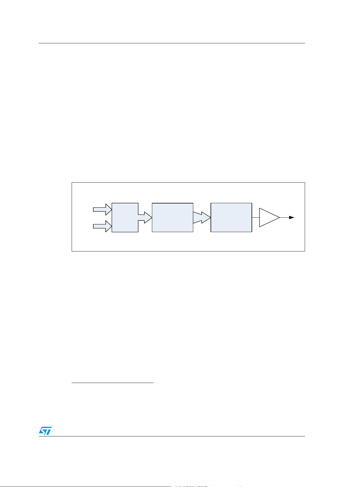
RC OSCILLATOR
DECODER
CLK_HSITRIM
HSI Clock Output
+
INIT_TR IM
1 High speed internal oscillator trimming
1.1 Introduction
The STM8S and STM8A 8-bit microcontrollers can use a high speed internal (HSI) RC
oscillator as a system clock source. This oscillator has a nominal frequency, f
16 MHz which is factory calibrated at an ambient temperature of T
voltage of V
= 5 V. This accuracy is specified in the datasheet for each device.
CC
= 25 °C and a supply
A
HSI nominal
The HSI frequency is calibrated to give reasonable accuracy for the vast majority of
applications. However, the output frequency of the RC oscillator is affected by temperature
and/or voltage drift, while, total accuracy of the HSI frequency is reduced a percentage
given in the datasheet. To compensate for such influences in the application, the STM8S
and STM8A HSI oscillator output frequency can be trimmed by the user runtime calibration
routine to improve frequency accuracy. This is especially important for communication
peripherals.
Figure 1. STM8S and STM8A HSI trimming principle
, of
Initial calibration data, INIT_TRIM, are stored in the protected part of the internal memory
and loaded onto the internal calibration register after reset.
The frequency of the HSI RC oscillator can be fine-tuned to achieve better accuracy with
wider temperature and supply voltage ranges. The lowest three bits of the CLK_HSITRIMR
register are reserved for this purpose. The number stored in these bits is processed as a
signed number with the two's-complement representation (see Ta bl e 1 ). The trimming
number
(a)
can vary from -4 (100b) to +3 (011b). This number is added to the factory
calibration value.
Note: An increase in this trimming value causes a decrease in HSI frequency.
The frequency change per step is approximately 1%
a. Some selected STM8S and STM8A devices can be set to 4-bit trimming mode by the HSITRIM option byte,
see device datasheet for details.
b. If the 4-bit trimming mode is set by the HSITRIM option byte, the frequency change between two steps in the
trimming value is approx. 0.5%
(b)
.
Doc ID 14983 Rev 2 5/19
Page 6
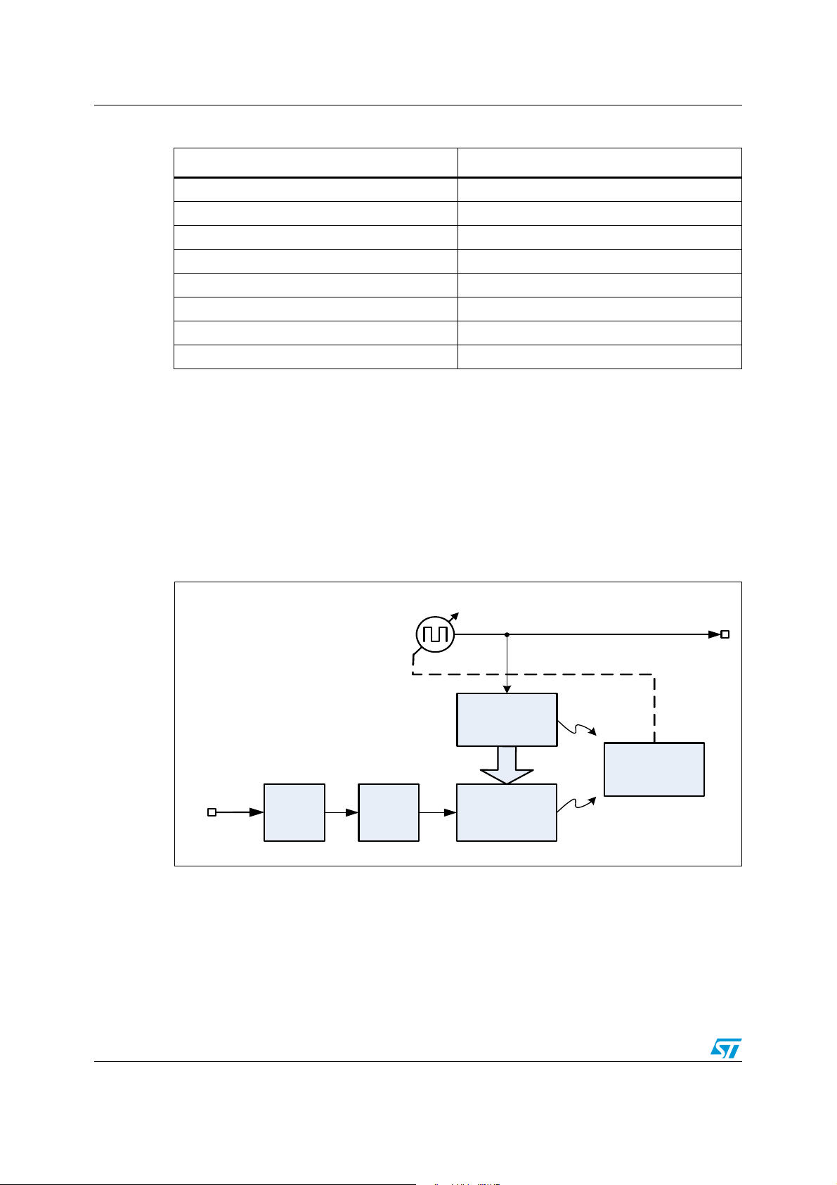
High speed internal oscillator trimming AN2822
TIM3_CC1
/1, /2, /4 or /8
Counter
Capture
f
MASTER
= f
HSI
Core
CCO
Overload
interrupt
Capture
interrupt
CLK_HSITRIMR
HSI 16 MHz
Prescaler
Calibration
signal
Input
Filter
TI1 TI1F IC1PS
Table 1. CLK_HSITRIMR values and two’s-complement binary representation
Decimal value Binary two’s-complement value
3011
2010
1001
0000
-1 111
-2 110
-3 101
-4 100
Note: The default value on the CLK_HSITRIMR register is zero (000b) after reset.
1.2 Calibration principle
To calibrate the HSI output frequency, a reference timebase is necessary. A simple
reference timebase can be used, such as the post-processed signal from the mains power
source (see Section 2). The final accuracy of the HSI frequency is strongly dependent on
the accuracy of the reference timebase. Better accuracy can be achieved with more
accurate timebases such as a signal generator.
Figure 2. HSI calibration set-up
The calibration signal, from the mains power supply, is connected to the TIM3_CC1 input pin
and is used as a timebase which allows the microcontroller to test if the HSI RC oscillator
frequency is above or below the nominal frequency. The HSI frequency is sequentially tuned
by the microcontroller until the optimum value is reached.
6/19 Doc ID 14983 Rev 2
Page 7

AN2822 High speed internal oscillator trimming
IdealCountedValue f
HSI nominalTcal
× L×=
The HSI frequency is evaluated from the number of pulses counted by timer TIM3 during
certain calibration signal periods. For noisy mains, where positive and negative half-periods
are not necessarily symmetrical, it is better to measure the whole period and not only the
time difference between the rising and falling edge of the calibration signal.
It is better to measure the number of HSI pulses for several sequential periods to reduce the
uncertainty of the measurement. This is also recommended when using a noisy mains as
the calibration signal. The input capture prescaler can be used for this purpose. It allows
every 1st, 2nd, 4th, or 8th rising edge of the calibration signal to be selected which is then
used to define the time interval for counting HSI pulses. In this way TIM3 is able to store
information about the number of HSI pulses in the capture register at the beginning and at
the end of a measurement.
If required (for example, for validation purposes), the frequency of the HSI oscillator can be
observed on the configurable clock output (CCO) pin.
See Section 2 for an example of a simple post-processing circuit which adapts a mains
signal to a square signal and converts the mains voltage to 5 V power supply voltage.
1.3 Calibration routine
The calibration routine is written in ANSI C. It takes advantage of the STM8S and STM8A
firmware library which is available from www.st.com. It can be simplified and optimized if
needed.
The software compares the number of HSI clock pulses during the certain number L of
calibration period, T
(20 ms), with the ideal value (see equation below).
cal
Using this equation, the calibration routine software compares the ideal HSI clock pulse
value (IdealCountedValue) with the nominal oscillator frequency, f
defined calibration period, T
(20 ms), for a known number of calibration signal periods (L).
cal
HSInominal
, during a
Note: For example, if the nominal HSI frequency is 16 MHz, the defined calibration period, T
20 ms (if the mains has a frequency of 50 Hz), and the known number of calibration signal
periods, L, is 8 then the ideal value captured by the timer is 2 560 000 (0x271000)
The calibration algorithm is described in Figure 3.
Calibration starts with initialization of TIM3. The lowest frequency is set by writing
MAX_TRIM_VAL to the CLK_HSITRIMR register. In this way, the trimming value is
decreased in the program loop. The difference between the number of counted HSI pulses
and the ideal value is compared with the previous difference, until either the current
difference becomes greater than the preceding difference, or, until the minimum value
MIN_TRIM_VAL is reached.
If the new difference is greater than the preceding difference, the trimming value is
incremented to the previous value, resulting in the optimum value for calibration.
cal
, is
Doc ID 14983 Rev 2 7/19
Page 8

High speed internal oscillator trimming AN2822
prevDiff
<
actDiff
Increment
CLK_HSITRIM
End of Calibration
Yes
No
Start of Calibration
CLK_HSITRIM = MAX_TRIM_VAL
Initialization of TIM3
Measure the HSI pulses,
Calculate abs (actual – ideal),
store it in prevDiff
CLK_HSITRIM
MIN_TRIM_VAL
Yes
No
Decrement
CLK_HSITRIM
Measure the HSI pulses
Calculate
1)
abs (actual – ideal)
Store it in actDiff
prevDiff = actDiff
Figure 3. HSI calibration flowchart
1. The ‘abs’ function calculates absolute value.
The measurement routine results are the sum of HSI pulses during the consequential
calibration period. The number of calibration signal periods, L, used for the measurement
are given by the constant, MAX_AVERAGED_PERIOD. The more periods used for the
measurement, the lower the uncertainty of period length due to the averaging effect. The
recommended value range is 4 or 8.
8/19 Doc ID 14983 Rev 2
Page 9

AN2822 High speed internal oscillator trimming
f
HSI
N
HSI
T
cal
L⋅
-------------------- -=
N
HSI
la stca p ture 0x 10000 overfl ows firstc aptur e–×+=
1.4 Measurement of HSI pulses per calibration period
The current HSI oscillator frequency, f
number of counted HSI clock pulses, N
, is not measured directly. It is evaluated from the
HSI
, during a defined calibration interval, T
HSI
cal
, for a
known number of calibration signal periods (L), using the following equation:
TIM3 timer counts the number of HSI pulses with minimum interaction from the software
routine. This helps to reduce measurement uncertainty caused by the software routine
reaction times. In addition, the MCU core is not occupied by the software and can continue
to execute user code.
The measurement of HSI pulses starts with the initialization of TIM3 timer. It is configured to
count the number of HSI pulses and to handle two interrupt events. The first interrupt occurs
when the timer overflows. The second interrupt is an input capture interrupt which occurs
every L
th
rising edge of the calibration period signal.
When the first rising edge of the calibration signal period occurs, the value in the
TIM3_CNTR register is stored in the input capture register, TIM3_CCR, and the content of
this register is saved during the input capture interrupt into the firstcapture variable.
The last input capture interrupt occurs when the L
th
rising edge of the calibration signal is
detected and the value in the input capture register TIM3_CCR is saved into the lastcapture
variable.
The number of overflows between the first and last capture events is increased at every
overflow interrupt and stored in the overflow variable.
When the last input capture event occurs the state MEASURE_COMPLETED is set and the
timer is stopped. Then the number of HSI pulses is evaluated using the equation below:
Figure 4 summarizes the measurement of HSI pulses for a known calibration signal period.
Doc ID 14983 Rev 2 9/19
Page 10

High speed internal oscillator trimming AN2822
Enter ‘overflow interrupt’
Exit interrupt
Increase the
number of
overflows
measureState
=
MEASURE_IN_
PROGRESS
YES
NO
measureState
?
Exit interrupt
Enter ‘input capture
interrupt’
MEASURE_START MEASURE_IN_PROGRESS
Disable interrupts
Stop the counter
Set measureState
to MEASURE_IN_
PROGRESS
Save Captured
value in
firstcapture
Set measureState
to MEASURE_
COMPLETED
Save Captured
value in
lastcapture
Initializing of
variables
Figure 4. Measurement of HSI pulses per calibration period flowchart
10/19 Doc ID 14983 Rev 2
Page 11

AN2822 High speed internal oscillator trimming
Counter
Register
Value
OVF
TI1
IC1PS
CC
OVL
OVL OVL
OVL
OVL
Filter Delay
L = 4
CC
OVL
1.5 Timing of calibration period measurement
This section describes the timing of the HSI oscillator frequency, f
measurement.
HSI
The ‘digital filtering technique’ is applied on the TI1 input from TIM3_CC1 (see Figure 2) to
further reduce period measurement uncertainty. This technique includes an event counter,
present on the input capture pin, in which a certain number of TI1 samples with the same
level are needed to validate a transition of the reference timebase. The number of such
pulses and the sampling frequency can be set by bits IC1F[3:0] in the TIM3_CCMR1
register. The sampling frequency can be set as an f
MASTER
eight equal consecutive samples with a time resolution of 1/f
divided by 1 to 32. By default,
MASTER
, are required for the
transition to be valid. This default value can be changed if needed. This digital filtering
technique causes a delay between TI1 and the IC1 signal. It does not affect the
measurement of HSI pulses per calibration interval (see Figure 5).
Figure 5. Timing diagram of calibration period measurement
Doc ID 14983 Rev 2 11/19
Page 12

High speed internal oscillator trimming AN2822
f
HSIm
N
HSI
L
------------ -
f
cal
=
uN
HSI
()
1
3
-------=
uf
cal
()
f
calδfcal
100 3
---------------------- -=
1.6 Uncertainty of calibrated HSI frequency
There are two sources of uncertainty
is caused by the finite resolution of the trimming value. The second is the uncertainty of the
HSI frequency measurement used to regulate HSI output frequency using the HSI trimming
register.
(c)
associated with this calibration method. The first one
The calibrated HSI oscillator frequency, f
, is not measured directly. We can start with
HSIm
the equation describing the estimated HSI frequency as a function of each of the factors that
can influence it to evaluate the uncertainty of the calibrated HSI output frequency given by
the calibration method
(d)
As L is a constant we can identify two uncertainty contributors. The first is a number of
counted HSI pulses, N
, the second is a calibration period, f
HSI
cal
.
These input parameters can be assumed as uncorrellated quantities.
The uncertainty of N
is caused by the nonsynchronous frequency of the calibration signal
HSI
and HSI oscillator frequency. The first rising edge of the L-series of calibration signal periods
can occur anywhere in the interval of one HSI signal period as well as the last rising edge
which close the counter gate, resulting in the uncertainty of counted HSI pulses equal to ±1.
Assuming uniform uncertainty distribution, the standard uncertainty of N
can be
HSI
evaluated using the following equation
To reduce this uncertainty, the calibration frequency should be well below the HSI frequency
(at least 1000 times lower). This is easily achieved when the mains frequency is used as a
calibration signal.
The uncertainty of the calibration signal frequency, f
mains frequency. Normally, the accuracy of the mains frequency, δf
, is given by the fluctuation of the
cal
, is better than ±1%.
cal
However, even better accuracy can be achieved by using a different frequency source, such
as a signal generator. To reduce uncertainty from this source to a minimum, the frequency
generator which gives the best accuracy should be used instead of the mains frequency.
The standard uncertainty of calibration frequency, f
, is expressed below assuming uniform
cal
uncertainty distribution.
From the equation describing the estimated HSI frequency, f
sensitivity coefficient associated with each of the input estimates.
c. This analysis of the HSI calibration method is based on ISO Guide to the Expression of Uncertainty in
Measurement and ANSI/NCSL Z540-2-1997. These standards offer a current international consensus of the
methods for estimating measurement uncertainty.
d. Estimates of uncertainty obtained in this way are usually called Type B.
12/19 Doc ID 14983 Rev 2
, we can calculate the
HSI
Page 13

AN2822 High speed internal oscillator trimming
c
N
HSI
N
HSI
∂
∂f
HSImfcal
L
--------==
c
f
cal
f
cal
∂
∂f
HSIm
N
HSI
L
------------ -==
u
c
2
f
HSIm
()c
i
2
ui()
2
i
∑
f
cal
L
--------
⎝⎠
⎛⎞
2
1
3
-------
⎝⎠
⎛⎞
2
N
HSI
L
------------ -
⎝⎠
⎛⎞
2
f
calδfcal
100 3
---------------------- -
⎝⎠
⎛⎞
2
+==
uf
trim
()
Δf
trim
23
--------------=
uf
HSI
() u2f
trim
()u
c
2
f
HSIm
()+=
uN
HSI
()
1
3
-------
1.732≅=
uf
cal
()
f
calδfcal
100 3
---------------------- -
50
100 3
-----------------
0.286≅==
c
N
HSI
N
HSI
∂
∂f
HSIm
f
cal
L
--------
12.5≅==
The combined standard uncertainty of the HSI frequency measurement can be calculated
by the equation bellow.
When the calibration is finished, the oscillator output frequency will be at maximum ±1/2 of
the frequency trimming step, Δf
steps causing additional uncertainty which can be expressed
, far from the desired frequency. This finite regulation
trim
(e)
by the following equation.
The total combined uncertainty of the HSI frequency can be expressed using the equation
below.
Example
Let’s consider as a calibration signal mains, f
δf
, in the range of ±1%, number of calibration signal periods L = 4 and a desired output
cal
, with a frequency of 50 Hz with accuracy,
cal
frequency 16 MHz. Evaluation of the uncertainty of input quantities and sensitivity
coefficients are the following.
e. Assuming a uniform distribution of the HSI output frequency uncertainty.
Doc ID 14983 Rev 2 13/19
Page 14

High speed internal oscillator trimming AN2822
c
f
cal
f
cal
∂
∂f
HSIm
N
HSI
L
------------ -
320 10⋅
3
468.7 8.376 109⋅()≅==
u
c
2
f
HSIm
()c
N
HSI
2u2
N
HSI
()c
f
cal
2u2
f
cal
()+ 468.7 8.376 109⋅+≅=
ucf
HSIm
()91.52 kHz≅
uf
trim
()
160 103⋅
23
--------------------------
46.19 kHz≅=
uf
HSI
() u2f
trim
()u
c
2
f
HSIm
()+ 102.5 kHz≅=
Ukuf
HSI
()⋅ 2 102.5 kHz 205 kHz≅⋅≅=
The combined standard uncertainty of the HSI frequency measurement is evaluated bellow.
Comparing the first and second terms we can find that a contribution caused by uncertainty,
u(N
), is negligible and can be omitted. This statement is valid if the calibration frequency
HSI
is well below the HSI frequency.
Let’s evaluate the uncertainty caused by the finite regulation steps.
Finally, the total combined uncertainty of the HSI frequency is evaluated bellow.
Assuming that the required confidence level is 95% using the coverage factor k=2, we can
express the extended uncertainty, U, as following.
14/19 Doc ID 14983 Rev 2
Page 15

AN2822 Power supply and calibration signal conditioning circuit
R2
C3
C1
+
R1
R4
V
DD
TIM3_CC1
STM8
N
L
AC Mains
~
D1
D2
C2
V
SS
R3
2 Power supply and calibration signal conditioning
circuit
Figure 6 shows the calibration signal conditioning circuit which also provides approximately
5 V of DC power supply to the microcontroller. Where power supply from the mains is not
needed, only a single resistor between power line and TIM3_CC1 input is adequate to
protect this pin from over current in normal operating conditions.
The calibration signal conditioning circuit contains a few passive components which convert
either the 230 V / 50 Hz of a European mains or the 110 V / 60 Hz of a US mains to a 5 V
DC power supply. An application with more current consumption should use a power
converter (see AN1357, VIPower: Low cost power supplies using VIPer12A in non isolated
applications).
Caution: The calibration signal conditioning and power supply circuits cannot be used if there are big
current variations.
Figure 6. Example of calibration signal conditioning circuit and 5 V power supply
If using a noisy mains, an input power line filter is recommended (see AN2326, Calibrating
the RC oscillator of the ST7ULTRALITE MCU using the mains).
Doc ID 14983 Rev 2 15/19
Page 16

Power supply and calibration signal conditioning circuit AN2822
Table 2. Value of used components
Component 230 V / 50 Hz value 110 V / 60 Hz value
R1 220 Ω / 0.5 W 110 Ω / 0.5 W
R2 220 Ω / 0.5 W 110 Ω / 0.5 W
R3 1 MΩ 1 MΩ
R4 5.6 kΩ 5.6 kΩ
D1 BZX85C5.6 BZX85C5.6
D2 1N4148 1N4148
C1 470 nF / ~275 V AC 330 nF / ~275 V AC
C2 100 nF 100 nF
C3 470 µF / 16 V 470 µF / 16 V
16/19 Doc ID 14983 Rev 2
Page 17

AN2822 Conclusion
3 Conclusion
The calibration method described in this application note, ensures that the high speed
internal clock of the STM8S and STM8A microcontrollers operates at its intended frequency
(16 MHz) in the target application, independently of the temperature and power supply
voltage drift.
The proposed solution uses the 16-bit timer TIM3 for measuring the internal RC oscillator
frequency and external calibration signal which can be easily adapted from the mains. An
implementation example with power supply and calibration signal conditioning circuit is
proposed.
The example source code written in ANSI C and using the STM8S and STM8A firmware
library can be download from www.st.com.
Doc ID 14983 Rev 2 17/19
Page 18

Revision history AN2822
4 Revision history
Table 3. Document revision history
Date Revision Changes
20-Jan-2009 1 Initial release
31-Aug-2011 2 Updated to refer to STM8S and STM8A products.
18/19 Doc ID 14983 Rev 2
Page 19

AN2822
Please Read Carefully:
Information in this document is provided solely in connection with ST products. STMicroelectronics NV and its subsidiaries (“ST”) reserve the
right to make changes, corrections, modifications or improvements, to this document, and the products and services described herein at any
time, without notice.
All ST products are sold pursuant to ST’s terms and conditions of sale.
Purchasers are solely responsible for the choice, selection and use of the ST products and services described herein, and ST assumes no
liability whatsoever relating to the choice, selection or use of the ST products and services described herein.
No license, express or implied, by estoppel or otherwise, to any intellectual property rights is granted under this document. If any part of this
document refers to any third party products or services it shall not be deemed a license grant by ST for the use of such third party products
or services, or any intellectual property contained therein or considered as a warranty covering the use in any manner whatsoever of such
third party products or services or any intellectual property contained therein.
UNLESS OTHERWISE SET FORTH IN ST’S TERMS AND CONDITIONS OF SALE ST DISCLAIMS ANY EXPRESS OR IMPLIED
WARRANTY WITH RESPECT TO THE USE AND/OR SALE OF ST PRODUCTS INCLUDING WITHOUT LIMITATION IMPLIED
WARRANTIES OF MERCHANTABILITY, FITNESS FOR A PARTICULAR PURPOSE (AND THEIR EQUIVALENTS UNDER THE LAWS
OF ANY JURISDICTION), OR INFRINGEMENT OF ANY PATENT, COPYRIGHT OR OTHER INTELLECTUAL PROPERTY RIGHT.
UNLESS EXPRESSLY APPROVED IN WRITING BY TWO AUTHORIZED ST REPRESENTATIVES, ST PRODUCTS ARE NOT
RECOMMENDED, AUTHORIZED OR WARRANTED FOR USE IN MILITARY, AIR CRAFT, SPACE, LIFE SAVING, OR LIFE SUSTAINING
APPLICATIONS, NOR IN PRODUCTS OR SYSTEMS WHERE FAILURE OR MALFUNCTION MAY RESULT IN PERSONAL INJURY,
DEATH, OR SEVERE PROPERTY OR ENVIRONMENTAL DAMAGE. ST PRODUCTS WHICH ARE NOT SPECIFIED AS "AUTOMOTIVE
GRADE" MAY ONLY BE USED IN AUTOMOTIVE APPLICATIONS AT USER’S OWN RISK.
Resale of ST products with provisions different from the statements and/or technical features set forth in this document shall immediately void
any warranty granted by ST for the ST product or service described herein and shall not create or extend in any manner whatsoever, any
liability of ST.
ST and the ST logo are trademarks or registered trademarks of ST in various countries.
Information in this document supersedes and replaces all information previously supplied.
The ST logo is a registered trademark of STMicroelectronics. All other names are the property of their respective owners.
© 2011 STMicroelectronics - All rights reserved
STMicroelectronics group of companies
Australia - Belgium - Brazil - Canada - China - Czech Republic - Finland - France - Germany - Hong Kong - India - Israel - Italy - Japan -
Malaysia - Malta - Morocco - Philippines - Singapore - Spain - Sweden - Switzerland - United Kingdom - United States of America
www.st.com
Doc ID 14983 Rev 2 19/19
 Loading...