

Page 1
AN2821
Application note
Clock/calendar implementation
on the STM32F10xxx microcontroller RTC
The internal RTC (real-time clock) of the 32-bit, ARM® Cortex™-M3-based medium-density
STM32F10xxx microcontroller is an independent timer. It provides a set of continuously
running counters, which, using suitable software, can be used to implement a clock/calendar
function. The RTC and backup registers are supplied through a switch that draws power
from either the V
when the main supply is switched off.
This application note gives an example of how to implement the clock/calendar functionality
using the medium-density STM32F10xxx microcontroller in low-power and standard
applications. The firmware example also performs leap year counting and tamper time
stamping. It provides a low-power mode demonstration and a basic RTC calibration routine
to compensate for crystal and temperature variations.
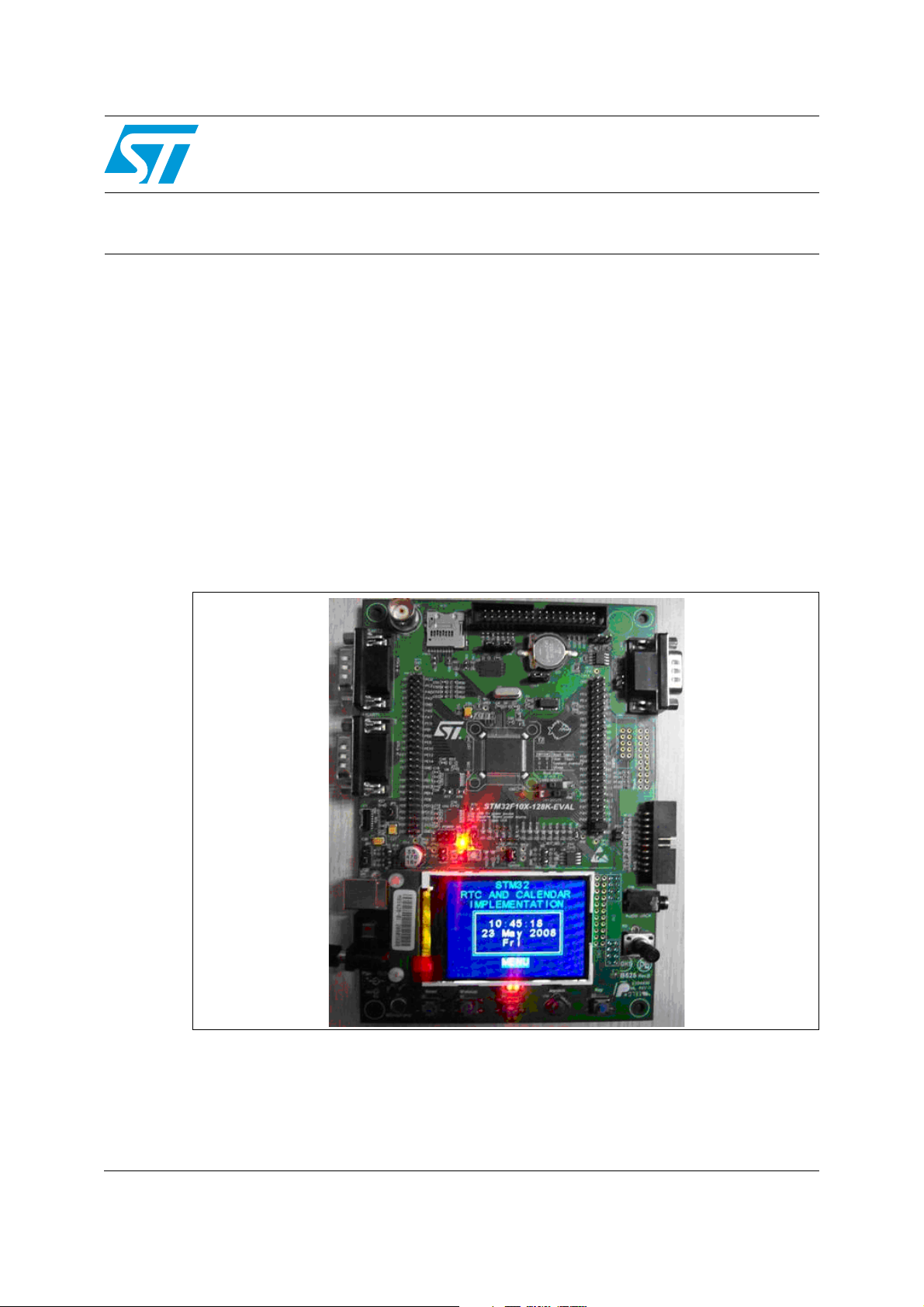
The STM3210B-EVAL board supports the firmware example described in this application
note without any modification to its hardware.
Figure 1. STM3210B-EVAL board
supply (when present) or the backup battery. Thus the RTC runs even
DD
April 2009 Doc ID 14949 Rev 2 1/28
www.st.com
Page 2

Contents AN2821
Contents
1 Overview of the medium-density STM32F10xxx backup domain . . . . . 6
1.1 Main backup domain features . . . . . . . . . . . . . . . . . . . . . . . . . . . . . . . . . . 6
1.2 Main RTC features . . . . . . . . . . . . . . . . . . . . . . . . . . . . . . . . . . . . . . . . . . . 7
2 Configuring the RTC registers . . . . . . . . . . . . . . . . . . . . . . . . . . . . . . . . . 8
3 Clock/calendar functionality features . . . . . . . . . . . . . . . . . . . . . . . . . . . 9
3.1 Clock/calendar basics . . . . . . . . . . . . . . . . . . . . . . . . . . . . . . . . . . . . . . . . 9
3.1.1 Implementing the clock function on the medium-density STM32F10xxx . 9
3.1.2 Implementing calendar function on the medium-density STM32F10xxx . 9
3.1.3 Summer time correction . . . . . . . . . . . . . . . . . . . . . . . . . . . . . . . . . . . . . 11
3.2 Clock source selection . . . . . . . . . . . . . . . . . . . . . . . . . . . . . . . . . . . . . . . 11
3.3 Calibration . . . . . . . . . . . . . . . . . . . . . . . . . . . . . . . . . . . . . . . . . . . . . . . . 11
3.4 Low-power modes . . . . . . . . . . . . . . . . . . . . . . . . . . . . . . . . . . . . . . . . . . 13
3.4.1 Stop mode . . . . . . . . . . . . . . . . . . . . . . . . . . . . . . . . . . . . . . . . . . . . . . . 13
3.4.2 Standby mode . . . . . . . . . . . . . . . . . . . . . . . . . . . . . . . . . . . . . . . . . . . . 14
3.5 Tamper detection and time stamping . . . . . . . . . . . . . . . . . . . . . . . . . . . . 15
3.5.1 TAMPER-RTC pin functionality . . . . . . . . . . . . . . . . . . . . . . . . . . . . . . . 15
3.5.2 Tamper timestamping . . . . . . . . . . . . . . . . . . . . . . . . . . . . . . . . . . . . . . 15
3.5.3 Battery tamper timestamping . . . . . . . . . . . . . . . . . . . . . . . . . . . . . . . . . 15
4 Firmware description . . . . . . . . . . . . . . . . . . . . . . . . . . . . . . . . . . . . . . . 16
5 Hardware description . . . . . . . . . . . . . . . . . . . . . . . . . . . . . . . . . . . . . . . 17
6 Running the demonstrator . . . . . . . . . . . . . . . . . . . . . . . . . . . . . . . . . . . 18
6.1 Clock/calendar . . . . . . . . . . . . . . . . . . . . . . . . . . . . . . . . . . . . . . . . . . . . . 18
6.1.1 Setting the time . . . . . . . . . . . . . . . . . . . . . . . . . . . . . . . . . . . . . . . . . . . 18
6.1.2 Setting the alarm . . . . . . . . . . . . . . . . . . . . . . . . . . . . . . . . . . . . . . . . . . 18
6.1.3 Setting the date . . . . . . . . . . . . . . . . . . . . . . . . . . . . . . . . . . . . . . . . . . . 18
6.2 Low-power demonstration . . . . . . . . . . . . . . . . . . . . . . . . . . . . . . . . . . . . 18
6.1.4 Summer time correction . . . . . . . . . . . . . . . . . . . . . . . . . . . . . . . . . . . . . 18
6.2.1 Stop mode . . . . . . . . . . . . . . . . . . . . . . . . . . . . . . . . . . . . . . . . . . . . . . . 18
6.2.2 Standby mode . . . . . . . . . . . . . . . . . . . . . . . . . . . . . . . . . . . . . . . . . . . . 19
2/28 Doc ID 14949 Rev 2
Page 3

AN2821 Contents
6.3 Timestamping . . . . . . . . . . . . . . . . . . . . . . . . . . . . . . . . . . . . . . . . . . . . . . 19
6.3.1 Tamper events . . . . . . . . . . . . . . . . . . . . . . . . . . . . . . . . . . . . . . . . . . . . 19
6.3.2 Battery removal and installation . . . . . . . . . . . . . . . . . . . . . . . . . . . . . . . 19
6.4 Clock calibration . . . . . . . . . . . . . . . . . . . . . . . . . . . . . . . . . . . . . . . . . . . . 20
6.5 Clock source selection . . . . . . . . . . . . . . . . . . . . . . . . . . . . . . . . . . . . . . . 20
6.5.1 50 Hz time base selection . . . . . . . . . . . . . . . . . . . . . . . . . . . . . . . . . . . 21
6.5.2 60 Hz time base selection . . . . . . . . . . . . . . . . . . . . . . . . . . . . . . . . . . . 21
Appendix A Calibration table. . . . . . . . . . . . . . . . . . . . . . . . . . . . . . . . . . . . . . . . . 23
Appendix B Additional notes on calibration and clock accuracy . . . . . . . . . . . 25
7 Revision history . . . . . . . . . . . . . . . . . . . . . . . . . . . . . . . . . . . . . . . . . . . 27
Doc ID 14949 Rev 2 3/28
Page 4

List of tables AN2821
List of tables
Table 1. Calibration lookup table . . . . . . . . . . . . . . . . . . . . . . . . . . . . . . . . . . . . . . . . . . . . . . . . . . . 23
Table 2. Document revision history . . . . . . . . . . . . . . . . . . . . . . . . . . . . . . . . . . . . . . . . . . . . . . . . . 27
4/28 Doc ID 14949 Rev 2
Page 5

AN2821 List of figures
List of figures
Figure 1. STM3210B-EVAL board . . . . . . . . . . . . . . . . . . . . . . . . . . . . . . . . . . . . . . . . . . . . . . . . . . . . 1
Figure 2. RTC block diagram . . . . . . . . . . . . . . . . . . . . . . . . . . . . . . . . . . . . . . . . . . . . . . . . . . . . . . . . 6
Figure 3. Time system flowchart
Figure 4. Calendar algorithm . . . . . . . . . . . . . . . . . . . . . . . . . . . . . . . . . . . . . . . . . . . . . . . . . . . . . . . 10
Figure 5. Leap year flowchart . . . . . . . . . . . . . . . . . . . . . . . . . . . . . . . . . . . . . . . . . . . . . . . . . . . . . . 10
Figure 6. Calibration process . . . . . . . . . . . . . . . . . . . . . . . . . . . . . . . . . . . . . . . . . . . . . . . . . . . . . . . 12
Figure 7. Stop mode entry sequence . . . . . . . . . . . . . . . . . . . . . . . . . . . . . . . . . . . . . . . . . . . . . . . . . 13
Figure 8. Standby mode entry sequence . . . . . . . . . . . . . . . . . . . . . . . . . . . . . . . . . . . . . . . . . . . . . . 14
Figure 9. STM3210B-EVAL board description . . . . . . . . . . . . . . . . . . . . . . . . . . . . . . . . . . . . . . . . . . 17
Figure 10. RTC time base connection . . . . . . . . . . . . . . . . . . . . . . . . . . . . . . . . . . . . . . . . . . . . . . . . . 21
Figure 11. Clock source selection . . . . . . . . . . . . . . . . . . . . . . . . . . . . . . . . . . . . . . . . . . . . . . . . . . . . 22
(1)
. . . . . . . . . . . . . . . . . . . . . . . . . . . . . . . . . . . . . . . . . . . . . . . . . . . 9
Doc ID 14949 Rev 2 5/28
Page 6
Overview of the medium-density STM32F10xxx backup domain AN2821
1 Overview of the medium-density STM32F10xxx
backup domain
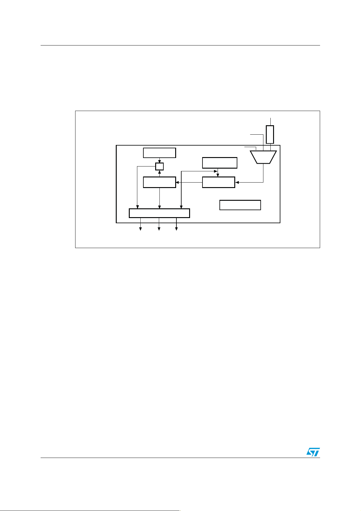
Figure 2 shows the RTC block diagram.
Figure 2. RTC block diagram
HSE OSC
RTC alarm
=
RTC counter
RTC control register
AlarmITOverflowITSecond
IT
1.1 Main backup domain features
The backup domain of the medium-density STM32F10xxx:
● includes ten 16-bit backup data registers, backup control/status registers and RTC
registers.
● is powered by V
● is not reset due to system reset, power reset or when the microcontroller wakes up
from the Standby mode.
● is protected from parasitic write access after reset (access to the backup domain is
disabled after reset)
● consists of two main units:
– an APB1 interface used to interface with the APB1 bus. The backup domain
registers are accessible through the APB1 bus in read/write access mode.
– an RTC core which is clocked by the RTC clock.
when the VDD main power is switched off.
BAT
LSE OSC/ EXT CLOCK
RTC prescaler
RTC divider
Backup registers
LSI RC
RTCSel
[1:0]
1/128
f
rtc
ai15437
6/28 Doc ID 14949 Rev 2
Page 7

AN2821 Overview of the medium-density STM32F10xxx backup domain
1.2 Main RTC features
The RTC:
● has three clock sources:
– LSE (low-speed external) clock that can also be bypassed by an external clock
– LSI (low-speed internal) RC oscillator
– HSE (high-speed external) clock divided by 128.
● has a 20-bit programmable prescaler that can be programmed to generate the RTC
time base. The prescaler load register contains the period counting value of the
prescaler.
● has three interrupt sources:
– second
–overflow
– alarm (also connected to EXTI Line 17 for auto-wakeup from Stop mode)
● its clock can be output on the TAMPER-RTC pin for calibration purposes.
Please refer to Figure 2 for an illustration of the medium-density STM32F10xxx RTC block
diagram.
All of the above mentioned features of the medium-density STM32F10xxx backup domain
can be used to develop a clock/calendar application equivalent to dedicated real-time
clocks.
Note: Be careful when choosing the 32.768 kHz crystal for your application. It is strongly
recommended to use a crystal with a load capacitance less than or equal to 7 pF. Never use
a crystal with a load capacitance of 12.5 pF.
Doc ID 14949 Rev 2 7/28
Page 8

Configuring the RTC registers AN2821
2 Configuring the RTC registers
On startup, follow the steps below to configure the RTC to generate an interrupt every
second:
● Enable the APB1 backup domain and power interface clocks by writing the BKPEN and
PWREN bits to ‘1’ in the RCC_APB1ENR register
● Enable access to backup domain by writing the DBP bit to ‘1’ in the PWR_CR register
● Enable the LSE clock by writing the LSEON bit to ‘1’ (also write LSEBYP to “1” when
the external clock has to be bypassed)
● Poll the LSERDY flag in the RCC_BDCR register until the LSE clock is ready (if the
external crystal is used as the clock source).
● Select LSE as the RTC clock source by writing ‘01’ to the RTCSEL bits in the
RCC_BDCR register.
● Enable the RTC clock by setting the RTCEN bit in the RCC_BDCR register
● Poll the RSF bit in the RTC_CRL register until the RTC registers are synchronized (if a
50/60 Hz external clock source is used this step may take up to a minute to complete)
● Poll the RTOFF bit in the RTC_CRL register until the last operation on the RTC
registers is over
● Enable the RTC second global interrupt by setting the SECIE bit in the RTC_CRH
register
● Wait for the last task to complete
● Set the RTC prescaler value using the following formula:
f
= f
TRCLK
–f
–f
RTCCLK
RTCCLK
TRCLK
For example, if an external 32.768 kHz (32 kHz) crystal oscillator is used, set the
prescaler to 32767. If an external 50 Hz supply is used set the prescaler value to 49.
/(PRL[19:0]+1), where:
is the input clock frequency
is the time base generated from the prescaler block
8/28 Doc ID 14949 Rev 2
Page 9
AN2821 Clock/calendar functionality features
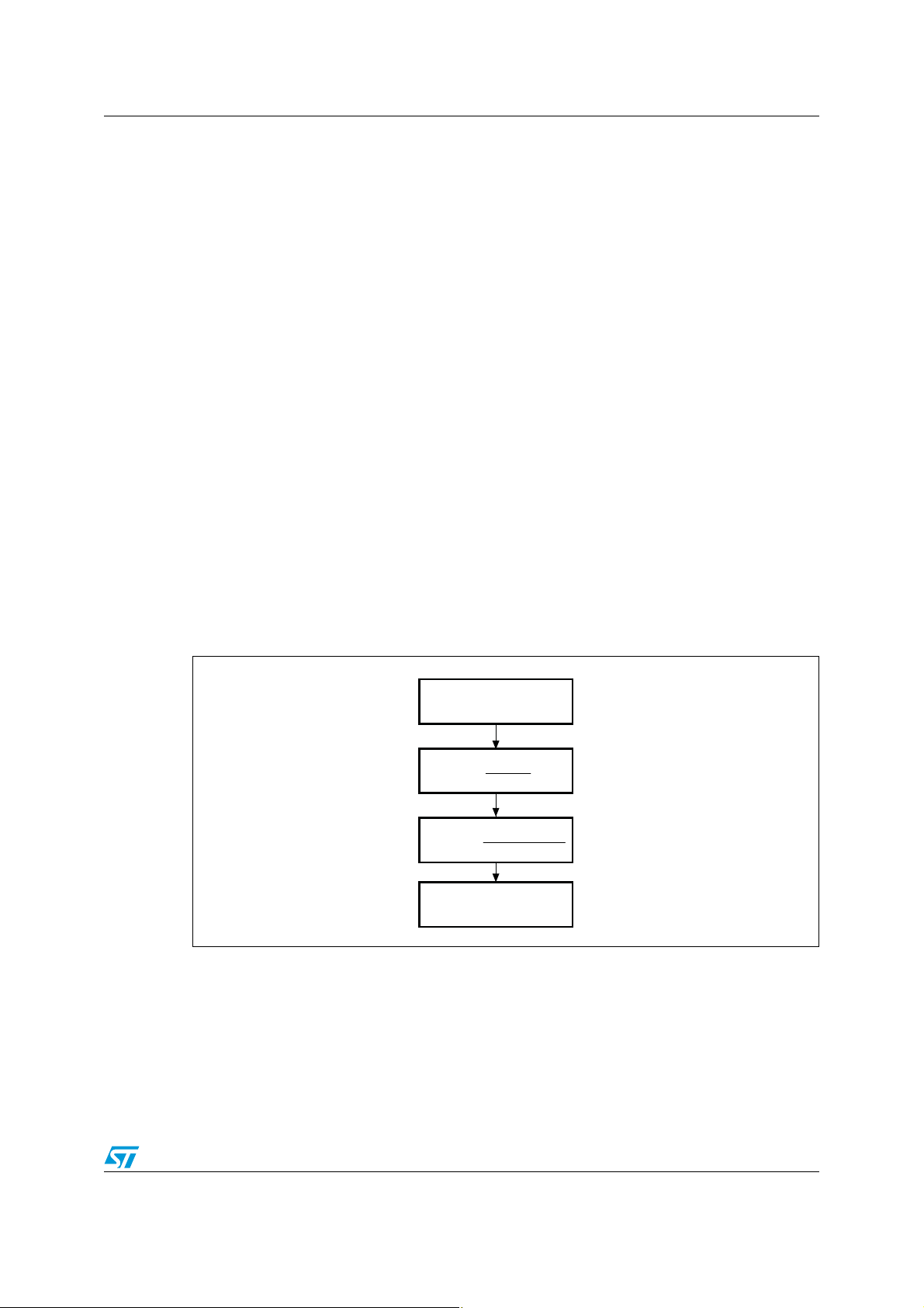
Read RTC counter value
(TimeVar)
ai15438
Hours = TimeVar
3600
Minutes = TimeVar % 3600
60
Seconds =
(TimeVar % 3600) % 60
3 Clock/calendar functionality features
3.1 Clock/calendar basics
A real-time clock keeps track of the time (hours, minutes, seconds) and date (day, month,
year). It should also take into account leap years. A leap year is a year where an extra day is
added to the calendar in order to synchronize it to the seasons. Since the tropical year is
365.242190 days long, a leap day must be added roughly once every 4 years (4 × 0.242190
= 0.968760). Thus, every four years, the month of February counts 29 days instead of 28.
3.1.1 Implementing the clock function on the medium-density STM32F10xxx
The used registers are RTC registers: prescaler register, counter register and alarm register.
The medium-density STM32F10xxx RTC peripheral consists of a chain of programmable
counters consisting of two main units:
● the RTC prescaler block generates the RTC time base. Depending on the clock period
applied to the LSE input, this prescaler can be adjusted to generate a time base
(RTC_CLK) of 1 second by writing to the prescaler load register.
● the 32-bit programmable counter can be initialized to the current system time. The
system time is incremented at the RTC_CLK rate and compared with the alarm register
value. When it reaches the alarm register value, an interrupt is generated.
The current system time can be inferred from the value in the counter register by following
the steps shown in Figure 3 (“/” implies division, “%” implies modulus)
Figure 3. Time system flowchart
1. % is for modulo.
(1)
3.1.2 Implementing calendar function on the medium-density STM32F10xxx
The used registers are the 16-bit backup data registers.
When the 32-bit counter register value reaches 86399, this means that one day has
elapsed, and that the date has to be updated. The counter value is then reset. Whenever the
system date is updated, the new date is stored into the 16-bit backup data registers so that
Doc ID 14949 Rev 2 9/28
Page 10

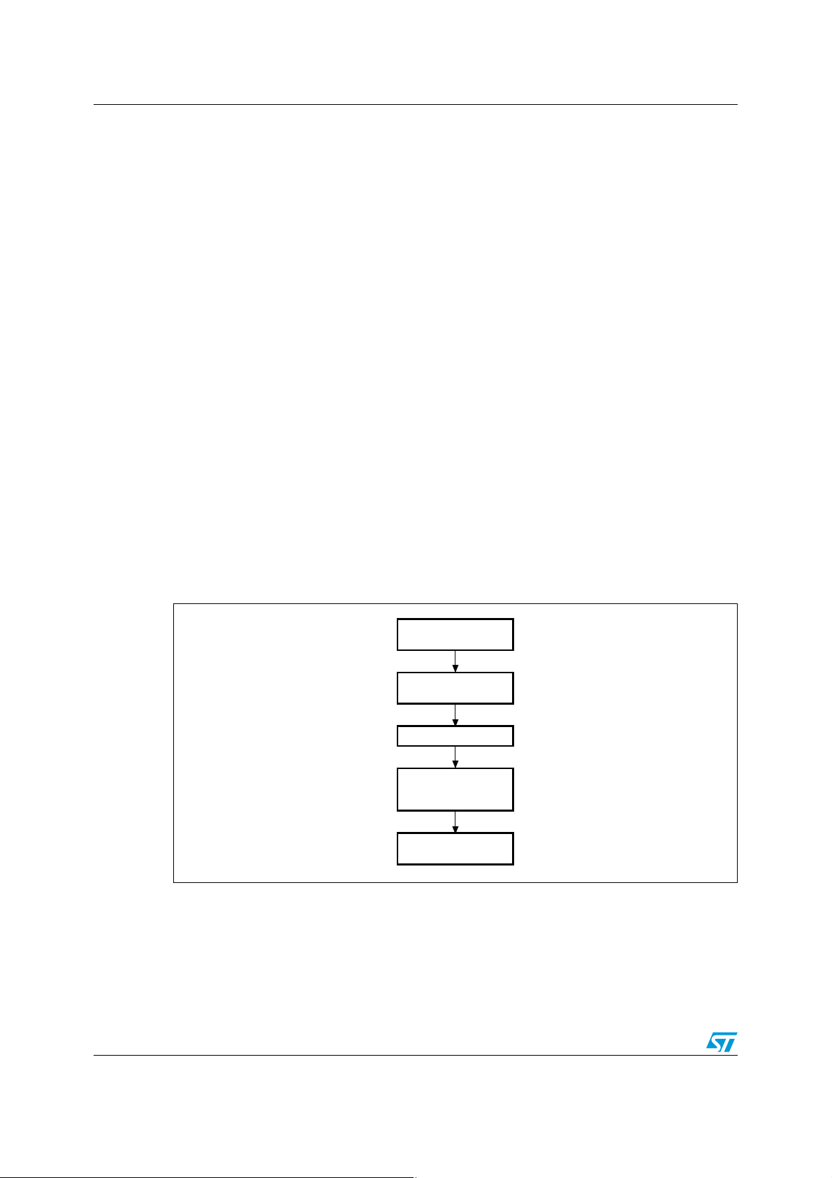
Clock/calendar functionality features AN2821
No
Year divisible
by 400?
Year divisible
by 100?
Yes
Year divisible
by 4?
It is a leap year
Yes
No
No
Not a leap year
ai15440
Not a leap year
It is a leap year
Yes
the system remains at the current date even after system reset, power reset or wakeup from
the Standby mode.
The calendar algorithm given in Figure 4 can be used to develop the date update function.
Figure 4. Calendar algorithm
No
Month has
31 days ?
Yes
Day < 31
?
No
Month = 12
?
Yes
Month=1
Day=1
Year++
Month has
30 days ?
Yes
?
No
Month++
Day=1
Yes
No
No
Yes
Day++
Month++
Day=1
Day++Day < 31
Month = 2
?
Yes
Day < 28?
No
Day = = 28
?
Yes
Is it a
leap year?
No
Month++
Day=1
Day = = 29
?
Yes
Month++
Day=1
Yes
No
Yes
Day++
Day++
ai15439
Leap year correction: each time the date is updated, the possibility of a leap year also has to
be considered (please refer to Figure 5).
Figure 5. Leap year flowchart
10/28 Doc ID 14949 Rev 2
Page 11

AN2821 Clock/calendar functionality features
Caution: In the case of a device in low-power mode or whose external supply is off when the counter
reaches 86399, the counter cannot be reset and so the date is not updated. This is why, just
after power reset, it is necessary to check the counter value and update the date as many
times as the number of days during which the device remained in low-power mode or had its
external main supply switched off.
3.1.3 Summer time correction
This correction is also known as daylight saving and it is used in some countries to save
power. The principle is to increment the time of a given country by an hour in summer time
so that the sun rises an hour later in the morning and daylight is present longer in the
evening. Typically, an hour is added to all clocks near the start of spring and, likewise, an
hour is removed in autumn. Exact time and date for summer time correction differs from
location to location.
3.2 Clock source selection
The external LSE (low-speed external) crystal oscillator can be a crystal oscillator usually
with a frequency of 32.768 kHz (
clock source to the RTC peripheral for clock calendar applications. The external LSE can
also be bypassed by an external clock. Thus, in countries where the mains power line
frequency is significantly stable, a 50 Hz or 60 Hz clock can also be used to provide the RTC
clock. Assuming that there is already an isolating circuit and an overcurrent protection in the
system, all that is needed is to bypass the LSE crystal and adjust the prescaler load register
value so as to generate a time base of 1 second, and hence the second interrupt, if
configured.
32 kHz), which provides a low-power and highly accurate
This application only covers the case of an emulated 50/60 Hz clock source.
The RTC time base of 1 second is derived from the following formula:
● f
● f
50 Hz selection: the prescaler load register value is set to 49 (0x31)
60 Hz selection: the prescaler load register value is set to 59 (0x3B)
32.768 kHz selection: the prescaler load register value is set to 32767 (0x7FFF).
3.3 Calibration
Real-clock precision is a requirement in most embedded applications. The external crystal
oscillator used to provide the time base is subject to frequency variations due to external
conditions. It is therefore necessary to compensate for crystal and temperature variations.
The calibration routine used in this application is based on RTC calibration as described in
application note AN2604.
The medium-density STM32F10xxx RTC comes with a digital calibration circuit that gives
the user software control over the calibration process. The digital calibration circuit removes
0 to 127 cycles every 2
on the value loaded into the seven least significant bits of the RTC clock calibration register.
The calibration circuit can only subtract clock cycles, which means that only higher
f
TRCLK
TRCLK
RTCCLK
= f
RTCCLK
/(PRL[19:0]+1), where:
is the derived time base
is the clock frequency applied on the low-speed oscillator input
20
clock cycles. The number of times the pulses are blanked depends
Doc ID 14949 Rev 2 11/28
Page 12

Clock/calendar functionality features AN2821
Output RTC clock/64
on TAMPER-RTC pin
Calculate deviation
from 511.968 Hz
Find nearest
calibration value
Load the value into
calibration register
ai15441
Calculate error in ppm
(deviation/511.968)
× 1 million
frequencies can be compensated whereas lower frequencies cannot. The frequency range
that can be calibrated is [32772, 32768]. The workaround consists in setting the prescaler to
32766 (instead of 32767), in which case the frequency range that can be calibrated shifts
from [32772, 32768] to [32770, 32766].
The calibration process, illustrated in Figure 6, is the following:
First, the TAMPER-RTC pin functionality is disabled and the clock calibration register ASOS
and ASOE bits are cleared. The (RTC clock) /64) frequency is output on the TAMPER-RTC
pin by setting the CCO (clock calibration output) bit in the clock calibration register.
There are two modes of calibration: auto-calibration and manual calibration. Manual
calibration consists in actually measuring the LSE/64 value with an external calibrated
frequency counter, calculating and manually entering the calibration value via the joystick.
● Auto-calibration:
The frequency output on the TAMPER-RTC pin is fed to the timer input. The frequency
is calculated by using the PWM input mode of the medium-density STM32F10xxx
general-purpose timer peripheral. The calibration value to be entered in the calibration
register can be inferred on the basis of the deviation from 511.968 Hz (the calibration
table giving calibration values for various error values in ppm is given in Appendix A.)
● Manual calibration:
In this case, the frequency output on the TAMPER-RTC pin has to be measured by
using an external precision instrument. The calibration value has to be calculated, and
then entered manually using the joystick.
Note: 1 When the RTC clock/64 is output on the TAMPER-RTC pin, the tamper detection
functionality is not available.
2 When the auto-calibration feature is used, the obtained calibration accuracy depends on the
accuracy of the on-board HSE clock. This is because the HSE is used as the time base to
measure the LSE frequency. As a consequence, if a very accurate oscilloscope or
frequency counter is available, it is recommended to implement manual calibration.
Figure 6. Calibration process
12/28 Doc ID 14949 Rev 2
Page 13

AN2821 Clock/calendar functionality features
Select the regulator
state in Stop mode
Reset PDDS
Request _WFI()
or _WFE()
ai15442
Set the SLEEPDEEP
bit in the Cortex-M3
system control register
3.4 Low-power modes
After a system or power reset, the microcontroller is in Run mode. In this mode, the CPU is
clocked by HCLK, and the CPU and its peripherals are running. Several low-power modes
are available to save power when there is no need for the CPU to be running.
The medium-density STM32F10xxx low-power modes have no effect on the internal RTC,
whose counter values keep being updated. The RTC alarm can also be used to auto-wake
up the microprocessor from the low-power mode.
The Stop and Standby low-power modes are described in the following paragraphs.
3.4.1 Stop mode
In the Stop mode, the:
● CPU clock is off
● peripheral clocks, PLL, HSI, HSE are disabled
● SRAM and register contents are preserved
● RTC and IWDG are kept running
● voltage regulator can be on or in low-power mode
Any of the EXTI line source, RTC Alarm, PVD or USB Wakeup can be used to release the
microcontroller from the Stop mode. On exiting the Stop mode, the clock configuration
returns to its reset state (HSI used as the system clock).
Entering the Stop mode
The sequence used to enter the Stop mode is illustrated in Figure 7 and described below:
1. Select the regulator state in Stop mode through the LPDS bit in the PWR_CR register:
– LPDS = ‘0’, the regulator is ON
– LPDS = ‘1’, the regulator is in low-power mode
2. Reset the PDDS bit in PWR_CR
3. Set the SLEEPDEEP bit in the Cortex-M3 system control register
4. Request Wait for interrupt or Wait for event depending on how the Stop mode is
entered.
Figure 7. Stop mode entry sequence
Doc ID 14949 Rev 2 13/28
Page 14
Clock/calendar functionality features AN2821
Clear the WAKEUP flag
in PWR_CSR
Enable the WAKEUP
pin
Request _WFI()
ai15443
Set the SLEEPDEEP
bit in the Cortex-M3
system control register
Set the PDDS bit
After the microcontroller has exited the Stop mode, the basic reset and clock control circuitry
has to be reconfigured and access to the backup domain has to be re-enabled.
3.4.2 Standby mode
In the Standby mode, the:
● CPU clock is off
● SRAM and register contents are lost except for the backup domain
● RTC and IWDG keep running
● entire 1.8 V domain is off
● Exit through WAKEUP pin rising edge, RTC Alarm, external reset.
The Standby mode is exited on the WAKEUP signal’s rising edge, by external reset or by
triggering an RTC Alarm.
Entering the Standby mode
The sequence used to enter the Standby mode is illustrated in Figure 8 and described
below:
1. Clear the WAKEUP flag in the PWR_CSR register.
2. Enable the WAKEUP pin functionality by setting the EWUP bit in the PWR_CSR
register
3. Set the PDDS bit in PWR_CR
4. Set the SLEEPDEEP bit in the cortex system control register
5. Request Wait for interrupt
Figure 8. Standby mode entry sequence
The Standby mode is the lowest power consumption mode. After the microcontroller wakes
up from the Standby mode, program execution restarts in the same way as after a
system/power reset.
14/28 Doc ID 14949 Rev 2
Page 15

AN2821 Clock/calendar functionality features
3.5 Tamper detection and time stamping
The medium-density STM32F10xxx features an internal supervisor (in the backup domain)
that can be used to detect external tampering.
3.5.1 TAMPER-RTC pin functionality
The TAMPER-RTC pin generates a tamper detection event when the level applied to it
changes from ‘0’ to ‘1’ or from ‘1’ to ‘0’ depending on the TPAL bit in the backup control
register (BKP_CR). A tamper detection event resets all the backup data registers.
Configuring the TAMPER-RTC pin:
1. Set the TAMPER-RTC pin level by configuring the TPAL bit in the backup control
register
2. Enable the TAMPER-RTC pin interrupt by setting the TPIE bit in the backup
control/status register (BKP_CSR)
3. Enable the TAMPER-RTC pin by setting the TPE bit in the backup control register
(BKP_CR)
3.5.2 Tamper timestamping
The tamper detection feature and the RTC of the medium-density STM32F10xxx can be
used to timestamp the tamper events, that is, to store the exact time and date of each
tamper event. In this application note, the microprocessor’ s internal Flash memory was
emulated as an EEPROM. The last few pages of the Flash memory can be used to store
these timestamps. Every time a tamper event is detected, the backup data registers are
cleared, which means that after every tamper event the calendar information has to be
rewritten to the backup registers.
3.5.3 Battery tamper timestamping
Events like battery removal or battery installation can also be timestamped and stored into
the emulated EEPROM. For this purpose, the V
battery) can be connected to a general-purpose I/O. Configured in interrupt mode, this I/O
generates an interrupt on both the falling and rising edges of the V
battery removal and battery installation events. The exact times and dates of the events can
be stored into the memory.
pin (which is connected to the external
BAT
signal so as to detect
BAT
Doc ID 14949 Rev 2 15/28
Page 16

Firmware description AN2821
4 Firmware description
The example firmware consists of a clock/calendar driver that includes all the functions
needed to realize a clock and calendar application on the medium-density STM32F10xxx
RTC peripheral. Other features like RTC calibration, low-power mode demonstration,
timestamping for tamper detection and battery removal/installation and, clock source
selection (between external crystal and 50/60 Hz) are also supported by the clock/calendar
driver. The source code example is based on the STM32F10xxx standard peripheral library.
User include files:
● clock_calendar.h: contains the prototypes of the basic functions used to implement the
calendar function on the STM32F10xxx’s internal RTC. Also includes some macros for
summer-time correction, system start default time and date.
● application_rtc.h: contains the RCC_Configuration, GPIO_Configuration and
SystickConfig function prototypes.
● eeprom.h: contains the prototypes of the functions used to emulate EEPROM in the
STM32F10xxx’s internal Flash memory, and for the timestamping application.
● lcd.h: contains the prototypes of the functions used to drive the TFT LCD present on
the STM3210B-EVAL board.
● fonts.h: includes various LCD font size definitions.
● menu.h: contains the prototypes of the functions needed to implement the menu.
User source files:
● clock_calendar.c: contains the basic routines for calendar implementation and RTC
calibration.
● application_rtc.c: contains the routines for system clock, peripheral clock, GPIO and
Systick timer initialization.
● eeprom.c: contains the functions used to emulate EEPROM in the STM32F10xxx’s
internal Flash memory. The 1 Kbyte internal Flash memory page 124 (address
0x0801F000 – 0x0801F3FF) is used to store timestamping information. The page
address and size are defined in the eeprom.h header file.
● lcd.c: contains the functions used to drive the display on the STM3210B-EVAL board.
● menu.c: contains the functions used to implement the menu. Various features can be
accessed through the menu options displayed on the LCD screen.
16/28 Doc ID 14949 Rev 2
Page 17

AN2821 Hardware description
5 Hardware description
This application can be fully demonstrated on the STM3210B-EVAL board. The main
hardware sections used are:
● TFT LCD
● LED’s (LD1, LD2, LD3, LD4)
● Joystick
● Tamper switch
● Wakeup switch
● PA1, PC7, PC8, PC13 pads
Figure 9. STM3210B-EVAL board description
Doc ID 14949 Rev 2 17/28
Page 18

Running the demonstrator AN2821
6 Running the demonstrator
6.1 Clock/calendar
The home screen displays the clock, date and day on the LCD screen. The MENU provides
various options. When the application is run for the first time, some default settings are
applied. The current system time and date can be set using various MENU options.
Press joystick Sel to select, joystick right/left to move to the next/previous position and
joystick up/down to increment/decrement the value. If you want to exit the current menu, do
not press any key for eight seconds, the display will automatically return to the home screen.
6.1.1 Setting the time
To set the system time, go to MENU->Time, and use joystick up/down to
increment/decrement the value, joystick right/left to move to the next/previous position and
joystick Sel to set the time and return to the home screen. The clock will then start with the
newly set time.
6.1.2 Setting the alarm
To set the alarm, go to MENU->Alarm, use joystick left/right, and up/down to enter the alarm
time. Then, press Sel. The system will now prompt you to set the alarm date. Enter the
alarm date and press Sel. When the Alarm condition is reached, the LD1 LED (see Figure 9:
STM3210B-EVAL board description) lights up and ‘ALARM’ appears on the LCD screen.
After five seconds, LD1 turns off and the display returns to the home screen.
6.1.3 Setting the date
To set the system date, go to MENU->Date and enter the current date using the joystick.
After entering the date, press the joystick Sel button to set the current date and return to the
home screen. The updated date is then displayed on the screen.
If a wrong date is entered, an error message is displayed on the LCD screen.
6.1.4 Summer time correction
The clock is set ahead by 1 hour at 2 am on the last Sunday of March and it is delayed by 1
hour on the last Sunday of October. Assumedly, the correction for March has already been
done and the correction for October has to be done. This is a one-time assumption only,
further corrections being automatically handled. The date and time have to be after the
current system date and time, that is, for instance if the initial time and date were set to
12:00 hours, 1
but not earlier.
st
April, 2008, you can verify the time correction for October 2008 and beyond,
6.2 Low-power demonstration
6.2.1 Stop mode
To enter the Stop mode, go to MENU->LowPower->STOP and press Sel. The LD4 LED
(see Figure 9: STM3210B-EVAL board description) lights up and the MCU enters the Stop
18/28 Doc ID 14949 Rev 2
Page 19

AN2821 Running the demonstrator
mode. A confirmation message is displayed on the LCD screen. Press the joystick Sel
button to exit the Stop mode. LD4 turns off and the display returns to the home screen.
6.2.2 Standby mode
To enter the Standby mode, go to MENU->LowPower->STANDBY and press Sel. A
confirmation message is displayed on the screen. The Standby mode is exited by pressing
the Wakeup switch (see Figure 9: STM3210B-EVAL board description).
The RTC alarm can also be used to auto-wake up the microcontroller from the Stop or
Standby mode. For that purpose, first configure the RTC Alarm and then place the
microcontroller in a low-power mode. When the alarm sets off, the microprocessor wakes up
from the low-power mode.
6.3 Timestamping
6.3.1 Tamper events
To trigger a tamper event, press the B4 tamper switch on the STM3210B-EVAL board (see
Figure 9: STM3210B-EVAL board description).
6.3.2 Battery removal and installation
The battery removal and installation conditions are simulated on the STM3210B-EVAL
board. The “battery in place” condition is simulated by placing a jumper between PC7 and
PC8 whereas the “battery removed” condition is simulated by removing this jumper. PC7
and PC8 are available on the STM3210B-EVAL board (see Figure 9: STM3210B-EVAL
board description).
Viewing tamper events
To view the tamper log, go to MENU->Tamper->VIEW. If there is no tamper event stored,
the corresponding message is displayed on the LCD screen. A maximum of 64 events can
be stored. Each page shows up to 10 events. Subsequent pages can be displayed by
pressing the joystick SEL button. The tamper view screen is exited from the last page by
pressing the joystick SEL button once more.
Erasing the tamper log
The user can also erase the tamper log. To do so, go to MENU->Tamper->ERASE. This
erases the tamper log.
Since only a page (1 Kbyte) in Flash memory is used to store timestamps, a maximum of 64
timestamps can be stored. Whenever the 65
The LCD screen cannot display more than 10 events at a time. The difference between
timestamps created by pressing the tamper switch and battery tamper timestamps is that
the former type of timestamps shows a “seconds” field, whereas the others show “BI” or
“BO” (to mean “battery in” and “battery out”, respectively).
th
tamper occurs the memory page is erased.
Doc ID 14949 Rev 2 19/28
Page 20

Running the demonstrator AN2821
Note: The TAMPER-RTC pin functionality is not available:
●
when the user is navigating through the MENU options
●
when user is viewing the tamper log
●
during the calibration process
●
when the microprocessor is in a low-power mode
●
when the main VDD supply is off
6.4 Clock calibration
To calibrate the external oscillator in manual mode, do as follows:
● Go to MENU -> CALIBRATE-> MANUAL. A message appears on the LCD screen:
“LSE/64 is available on the PC13/TAMPER-RTC pin. Measure the frequency and press
Sel to proceed”.
The frequency output on the TAMPER-RTC pin can be measured by using a highprecision frequency counter. The PC13 pad is available on the STM3210B-EVAL
board. (Refer to Figure 9: STM3210B-EVAL board description.)
● Follow the steps of the procedure illustrated in Figure 6: Calibration process to
calculate the error in ppm. On the basis of this error, the calibration value can be
inferred from the Calibration lookup table in Appendix A.
Once this is done, press Sel. You will be prompted to enter the calibration value. To do
so, use the joystick up/down and left/right buttons, then press Sel again. If the entered
value is within the range (0-121), it is stored into the RTC clock/calibration register and
the application returns to the home screen. Otherwise, the value is invalid. This
generates an error message and the application returns to the home screen without
modifying the value in the RTC clock/calibration register.
To calibrate the external oscillator in auto-calibration mode, do as follows:
● First, connect a wire link from PC13 (RTC clock output on the TAMPER-RTC pin) to
PA1 (timer input). Both of these pads are available on the STM3210B-EVAL board.
(Refer to Figure 9: STM3210B-EVAL board description.)
● Select MENU->CALIBRATE->AUTO: the calibration value is automatically calculated
and fed into the calibration register. A confirmation message will appear on the LCD
screen.
● After the calibration process, the application returns to normal clock operation.
Note: For more details, please refer to Appendix B: Additional notes on calibration and clock
accuracy on page 25.
6.5 Clock source selection
By default, on startup the clock runs at the external crystal oscillator frequency of
32.768 kHz. This frequency is provided by the clock source of the STM3210B-EVAL board.
An external clock source can also be used to provide the time base for the RTC. Figure 10
shows how to realize the RTC time base circuit.
20/28 Doc ID 14949 Rev 2
Page 21

AN2821 Running the demonstrator
STM32F10xxx
50/60 Hz in
Resistive
divider
Source
switch
OSC in
OSC out
2 jumpers for source
selection, to GPIO
Jumper for anti-tamper
demonstration,
optional
display (part of main
system)
switches/joystick,
to set the time/date
(part of main system)
Backup battery
(part of main system)
32 kHz crystal
ai15444
Figure 10. RTC time base connection
In this application note, the clock source selection is demonstrated by emulating an external
50/60 Hz sinewave (as can be derived from the utility mains). The external 50/60 Hz can be
derived from a function generator and applied to the oscillator input using a connector probe
(see Figure 11: Clock source selection).
Caution: Make sure that the amplitude of the applied clock signal is less than 3 V peak-to-peak and
that the corresponding DC offset is about half the full-scale value.
Note: Since the time base selection is a one-time setting, the clock is initialized every time the time
base is changed.
6.5.1 50 Hz time base selection
To select an external 50 Hz clock source:
● Apply the external clock to the oscillator input. The clock will seem to stop running.
● Go to MENU->50Hz and press the joystick Sel button. This sets the prescaler
accordingly and the clock restarts from 09:24:00.
To return to the 32.768 kHz clock source selection:
● Go to MENU->32768Hz and press the joystick Sel button
● Remove the external clock source. The clock restarts from 09:24:00.
6.5.2 60 Hz time base selection
To select an external 60 Hz source:
● Apply the external clock to the oscillator input
● Go to MENU->60Hz and press the joystick Sel button. this sets the prescaler
accordingly and the clock restarts from 09:24:00.
To return to the 32.768 kHz clock source selection:
● Go to MENU->32768Hz and press the joystick Sel button
● Remove the external clock source. The clock restarts from 09:24:00.
Doc ID 14949 Rev 2 21/28
Page 22

Running the demonstrator AN2821
Figure 11. Clock source selection
22/28 Doc ID 14949 Rev 2
Page 23

AN2821 Calibration table
Appendix A Calibration table
Ta bl e 1 gives a list of calibration values.
Table 1. Calibration lookup table
Calibration
value
Value in ppm
rounded to the
nearest ppm
Value in seconds per
month (30 days) rounded
to the nearest second
Calibration
value
Value in ppm
rounded to the
nearest ppm
month (30 days) rounded
00 0 6461 158
11 2 6562 161
22 5 6663 163
33 7 6764 166
4 4 10 68 65 168
5 5 12 69 66 171
6 6 15 70 67 173
7 7 17 71 68 176
8 8 20 72 69 178
9 9 22 73 70 180
10 10 25 74 71 183
11 10 27 75 72 185
12 11 30 76 72 188
13 12 32 77 73 190
14 13 35 78 74 193
15 14 37 79 75 195
16 15 40 80 76 198
17 16 42 81 77 200
18 17 44 82 78 203
19 18 47 83 79 205
20 19 49 84 80 208
21 19 49 85 81 210
22 21 54 86 82 213
23 22 57 87 83 215
24 23 59 88 84 218
25 24 62 89 85 220
26 25 64 90 86 222
27 26 67 91 87 225
28 27 69 92 88 227
29 28 72 93 89 230
Value in seconds per
to the nearest second
Doc ID 14949 Rev 2 23/28
Page 24

Calibration table AN2821
Table 1. Calibration lookup table (continued)
Calibration
value
Value in ppm
rounded to the
nearest ppm
Value in seconds per
month (30 days) rounded
to the nearest second
Calibration
value
Value in ppm
rounded to the
nearest ppm
30 29 74 94 90 232
31 30 77 95 91 235
32 31 79 96 92 237
33 31 82 97 93 240
34 32 84 98 93 242
35 33 87 99 94 245
36 34 89 100 65 247
37 35 91 101 96 250
38 36 94 102 97 252
39 37 96 103 98 255
40 38 99 104 99 257
41 39 101 105 100 260
42 40 104 106 101 262
43 41 106 107 102 264
44 42 109 108 103 267
45 43 111 109 104 269
46 44 114 110 105 272
47 45 116 111 106 274
48 46 119 112 107 277
49 47 121 113 108 279
50 48 124 114 109 282
51 49 126 115 101 284
52 50 129 116 111 287
53 51 131 117 112 28
54 51 133 118 113 292
55 52 136 119 113 294
56 53 138 120 114 297
57 54 141 121 115 299
58 55 143 122 116 302
59 56 146 123 117 304
60 27 148 124 118 307
61 58 151 125 119 309
62 59 153 126 120 311
63 60 156 127 121 314
Value in seconds per
month (30 days) rounded
to the nearest second
24/28 Doc ID 14949 Rev 2
Page 25

AN2821 Additional notes on calibration and clock accuracy
dT
1
F0 dF+
-------------------- -
F0
-------------------- - 1 s–
1 s
-----------------------------------=
dT
1
32762.7648
-------------------------------
32766
------------------------------- 1 s–
1 s
--------------------------------------------- -=
Appendix B Additional notes on calibration and clock
accuracy
The purpose of this appendix is to provide an effective calibration and drift calculation
scheme by a mathematical approach.
It is easy to verify the actual (observed) result using the theoretical value obtained. The
procedure first consists in calculating how much the clock drifts ahead (due to crystal
frequency variation) in a month when not calibrated. This is the amount that the clock must
“lose” to keep time correctly.
Next, the procedure consists in calculating how much the clock actually loses as a result of
calibration.
Example of calculation
To implement this method, switch to calibration mode, and measure the frequency output on
the TAMPER-RTC pin using a suitable and very accurate frequency counter. Let F1 be the
result obtained with this counter. Let us assume that F1 = 512.0193 Hz.
Let F2 be the corresponding effective LSE frequency.
F2 = 64 × F1 = 64 × 512.0193 Hz = 32769.2352 Hz.
Let us put dF = F0 – F2, where F0 = 32766 in our case, because the RTC prescalor is set to
32766 and not 32768. This means that we get a tick every 32766 oscillator cycles.
Thus, dF = 32766 – 32769.2352 = –3.2352
Let us now calculate the time drift or deviation generated by crystal variations only. It is given
by:
that is:
= (1.00009875) – 1 = 0.00009875 s = 98.75 µs
So over 1 second, the positive time drift is of 98.75 µs.
Thus, over 1 month the drift becomes: 0.00009875 s × 60 × 60 × 24 × 30 = 255.95 s.
Let T1 be this positive time drift.
Therefore, if we want to compensate for this time drift, we must, as a result of the calibration
process, lose T1.
Doc ID 14949 Rev 2 25/28
Page 26

Additional notes on calibration and clock accuracy AN2821
Error in ppm
512.0193
32766
64
----------------–
32766
64
----------------
-----------------------------------------------
1000000 100.2 ppm==
number of seconds lost in 1 month
32766606024 30
2
20
--------------------------------------------------------------------
105
32766
------------------------------------------------------------------------------------ -
260 seconds =
Now let us look into the calibration process:
Referring to the calibration lookup table, the calibration value that corresponds to an error of
100.2 ppm is 105, which amounts to a compensation (subtraction) of 260 seconds. Let T2
be this compensation time.
(STM32 digital calibration subtracts [Calibration value] every 2
20
oscillator cycles. That is:
This means that the clock will run slower by (T2 – T1), that is 4 seconds at the end of a
month. Thus, ideally, an average drift of 4/30 (about 0.133) second a day is achievable.
You can refer to a precise and accurate web clock to synchronize your clock, for instance the
US Naval Observatory Master Clock (http://www.usno.navy.mil/).
Note: Temperature effects and measuring instrument accuracy are not taken into account in the
above calculations.
26/28 Doc ID 14949 Rev 2
Page 27

AN2821 Revision history
7 Revision history
Table 2. Document revision history
Date Revision Changes
23-Dec-2008 1 Initial release.
References to the STM32F10xxx firmware library updated to
30-Apr-2009 2
STM32F10xxx standard peripheral library.
Systick_Config updated to SystickConfig.
Doc ID 14949 Rev 2 27/28
Page 28

AN2821
Please Read Carefully:
Information in this document is provided solely in connection with ST products. STMicroelectronics NV and its subsidiaries (“ST”) reserve the
right to make changes, corrections, modifications or improvements, to this document, and the products and services described herein at any
time, without notice.
All ST products are sold pursuant to ST’s terms and conditions of sale.
Purchasers are solely responsible for the choice, selection and use of the ST products and services described herein, and ST assumes no
liability whatsoever relating to the choice, selection or use of the ST products and services described herein.
No license, express or implied, by estoppel or otherwise, to any intellectual property rights is granted under this document. If any part of this
document refers to any third party products or services it shall not be deemed a license grant by ST for the use of such third party products
or services, or any intellectual property contained therein or considered as a warranty covering the use in any manner whatsoever of such
third party products or services or any intellectual property contained therein.
UNLESS OTHERWISE SET FORTH IN ST’S TERMS AND CONDITIONS OF SALE ST DISCLAIMS ANY EXPRESS OR IMPLIED
WARRANTY WITH RESPECT TO THE USE AND/OR SALE OF ST PRODUCTS INCLUDING WITHOUT LIMITATION IMPLIED
WARRANTIES OF MERCHANTABILITY, FITNESS FOR A PARTICULAR PURPOSE (AND THEIR EQUIVALENTS UNDER THE LAWS
OF ANY JURISDICTION), OR INFRINGEMENT OF ANY PATENT, COPYRIGHT OR OTHER INTELLECTUAL PROPERTY RIGHT.
UNLESS EXPRESSLY APPROVED IN WRITING BY AN AUTHORIZED ST REPRESENTATIVE, ST PRODUCTS ARE NOT
RECOMMENDED, AUTHORIZED OR WARRANTED FOR USE IN MILITARY, AIR CRAFT, SPACE, LIFE SAVING, OR LIFE SUSTAINING
APPLICATIONS, NOR IN PRODUCTS OR SYSTEMS WHERE FAILURE OR MALFUNCTION MAY RESULT IN PERSONAL INJURY,
DEATH, OR SEVERE PROPERTY OR ENVIRONMENTAL DAMAGE. ST PRODUCTS WHICH ARE NOT SPECIFIED AS "AUTOMOTIVE
GRADE" MAY ONLY BE USED IN AUTOMOTIVE APPLICATIONS AT USER’S OWN RISK.
Resale of ST products with provisions different from the statements and/or technical features set forth in this document shall immediately void
any warranty granted by ST for the ST product or service described herein and shall not create or extend in any manner whatsoever, any
liability of ST.
ST and the ST logo are trademarks or registered trademarks of ST in various countries.
Information in this document supersedes and replaces all information previously supplied.
The ST logo is a registered trademark of STMicroelectronics. All other names are the property of their respective owners.
© 2009 STMicroelectronics - All rights reserved
STMicroelectronics group of companies
Australia - Belgium - Brazil - Canada - China - Czech Republic - Finland - France - Germany - Hong Kong - India - Israel - Italy - Japan -
Malaysia - Malta - Morocco - Philippines - Singapore - Spain - Sweden - Switzerland - United Kingdom - United States of America
www.st.com
28/28 Doc ID 14949 Rev 2
 Loading...