

Page 1

AN2804
Application note
Virtual current control loop for L9374-L9375
coil driver kit in ABS-ESC control unit
Introduction
In the conventional hydraulic modulator for ABS-ESC control units, the 6 inlet valves (also
known as ISO and/or TC-ISO valves), that is, the 4 devoted to the ABS/TCS functions and
the other 2 valves devoted to the ESC functions, need a strict control of the coil energizing
current. From the point of view of the electronic components involved in the ABS-ESC
system partitioning, the above specification means to have a coil driver kit with 6 current
regulated channels. The current regulation specification guarantees to have in the coil,
driving the opening/closing of the on-off solenoid valve, the same energizing current against
supply voltage changes, temperature gradient, "stiction" phenomena inside the valve due,
for instance, to the aging and/or waste of the hydraulic and mechanical components (e.g.
brake fluid, ball, armature, spring,…) involved into the valve working.
In this work, we propose a coil driver kit, composed by L9374-L9375, for new generation
ABS/ESC control unit. The L9374 is a smart quad low side driver with 2 current regulated
channels (accuracy is about 6%) and 2 PWM channels. On the other hand, the L9375 is an
octal low side driver having 4 PWM channels and 4 conventional on-off switch channels. In
order to allow the L9374-L9375 kit to work as there are 6 current regulated channels, we
conceived a SW library, implemented by ST10252M microcontroller, that exploits data
(these data are available on the MISO bus of the SPI) coming from the 2 current regulated
channels of L9374 to calibrate the 4 PWM channels of L9375 so that they can work as
having a current regulation loop. This virtual current control loop has been tested in different
working conditions of the coil drivers:
● considering different supply voltages during the calibration and during the actuation of
the virtual current regulated channels of L9375;
● simulating different temperature gradients;
● simulating temperature mismatches between the coil driven by a current regulated
channel of L9374 and the coil driven by a virtual current regulated channel of L9375;
● considering several calibration timing and current set-points;
● taking into account different hydraulic modulators (Bosch, TRW).
Basically, the results show a satisfactory behavior of the virtual current control loop. In all the
test conditions taken into account, it comes out an accuracy of the virtual current control
loop that is similar to the nominal accuracy of the 2 current regulated channels of the L9374.
July 2008 Rev 1 1/34
www.st.com
Page 2

Contents AN2804
Contents
1 L9374 and L9375 summary description . . . . . . . . . . . . . . . . . . . . . . . . . 5
2 VCCL: plan of accuracy evaluation . . . . . . . . . . . . . . . . . . . . . . . . . . . . . 7
3 ABS/ESC: load analysis . . . . . . . . . . . . . . . . . . . . . . . . . . . . . . . . . . . . . 10
4 Current measurement procedure: validation . . . . . . . . . . . . . . . . . . . . 11
5 VCCL accuracy evaluation . . . . . . . . . . . . . . . . . . . . . . . . . . . . . . . . . . . 12
6 VCCL: computational burden evaluation . . . . . . . . . . . . . . . . . . . . . . . 25
7 VCCL: fixed point arithmetic . . . . . . . . . . . . . . . . . . . . . . . . . . . . . . . . . 27
8 Acronyms . . . . . . . . . . . . . . . . . . . . . . . . . . . . . . . . . . . . . . . . . . . . . . . . . 32
9 Revision history . . . . . . . . . . . . . . . . . . . . . . . . . . . . . . . . . . . . . . . . . . . 33
2/34
Page 3

AN2804 List of tables
List of tables
Table 1. Characterization of the load seen by the L9374 vs. the current setpoint imposed
on the Q3 channel . . . . . . . . . . . . . . . . . . . . . . . . . . . . . . . . . . . . . . . . . . . . . . . . . . . . . . . 10
Table 2. Characterization of the procedure used to measure the current into the VCCL
validation tests . . . . . . . . . . . . . . . . . . . . . . . . . . . . . . . . . . . . . . . . . . . . . . . . . . . . . . . . . . 11
Table 3. VCCL accuracy evaluation with a spot calibration having a current setpoint
on the Q3 channel of L9374 equal to 700 mA . . . . . . . . . . . . . . . . . . . . . . . . . . . . . . . . . . 12
Table 4. VCCL accuracy evaluation in option 1A spot calibration versus power supply. . . . . . . . . . 14
Table 5. VCCL accuracy evaluation with a spot calibration having a current setpoint
on the Q3 channel of L9374 equal to 250 mA . . . . . . . . . . . . . . . . . . . . . . . . . . . . . . . . . . 17
Table 6. VCCL accuracy evaluation in option 1B spot calibration versus power supply. . . . . . . . . . 19
Table 7. VCCL accuracy evaluation in option 1A when a temperature mismatch of 20°
is simulated (Q5 channel of L9375) . . . . . . . . . . . . . . . . . . . . . . . . . . . . . . . . . . . . . . . . . . 21
Table 8. VCCL accuracy evaluation in option 1A when a temperature mismatch of 20°
is simulated (Q3 channel of L9375) . . . . . . . . . . . . . . . . . . . . . . . . . . . . . . . . . . . . . . . . . . 22
Table 9. VCCL accuracy evaluation in option 1B when a temperature mismatch of 20°
is simulated (Q5 channel of L9375) . . . . . . . . . . . . . . . . . . . . . . . . . . . . . . . . . . . . . . . . . . 22
Table 10. VCCL accuracy evaluation in option 1B when a temperature mismatch of 20°
is simulated (Q3 channel of L9375) . . . . . . . . . . . . . . . . . . . . . . . . . . . . . . . . . . . . . . . . . . 23
Table 11. Analysis of the error propagation in the VCCL_dc_calculation function call
versus different Isat value and current setpoints . . . . . . . . . . . . . . . . . . . . . . . . . . . . . . . . 28
Table 12. Acronyms . . . . . . . . . . . . . . . . . . . . . . . . . . . . . . . . . . . . . . . . . . . . . . . . . . . . . . . . . . . . . . 32
Table 13. Document revision history . . . . . . . . . . . . . . . . . . . . . . . . . . . . . . . . . . . . . . . . . . . . . . . . . 33
3/34
Page 4

List of figures AN2804
List of figures
Figure 1. L9374 application block diagram . . . . . . . . . . . . . . . . . . . . . . . . . . . . . . . . . . . . . . . . . . . . . 6
Figure 2. L9375 application block diagram . . . . . . . . . . . . . . . . . . . . . . . . . . . . . . . . . . . . . . . . . . . . . 6
Figure 3. Block diagram of the VCCL . . . . . . . . . . . . . . . . . . . . . . . . . . . . . . . . . . . . . . . . . . . . . . . . . 7
Figure 4. Details on the implementation of the VCCL accuracy evaluation plan . . . . . . . . . . . . . . . . . 8
Figure 5. Details on the spot calibration of the VCCL accuracy evaluation plan . . . . . . . . . . . . . . . . . 9
Figure 6. ABS/ESC 8.0 Bosch Hydraulic modulator and INLET valve section . . . . . . . . . . . . . . . . . 10
Figure 7. VCCL accuracy evaluation with a spot calibration having a current setpoint
on the Q3 channel of L9374 equal to 700 mA . . . . . . . . . . . . . . . . . . . . . . . . . . . . . . . . . . 13
Figure 8. VCCL accuracy evaluation in option 1A spot calibration versus power supply . . . . . . . . . 15
Figure 9.
Figure 10.
Figure 11. VCCL accuracy evaluation with a spot calibration having a current setpoint
Figure 12. VCCL accuracy evaluation in option 1B spot calibration versus power supply . . . . . . . . . 20
Figure 13.
Figure 14.
Figure 15. Sensitivity versus coil temperature in the option 1A VCCL. . . . . . . . . . . . . . . . . . . . . . . . . 23
Figure 16. Sensitivity versus coil temperature in the option 1B VCCL. . . . . . . . . . . . . . . . . . . . . . . . . 24
Figure 17. Details on the implementation of the VCCL . . . . . . . . . . . . . . . . . . . . . . . . . . . . . . . . . . . . 25
Figure 18. Details on the implementation of the VCCL_dc_calculation function . . . . . . . . . . . . . . . . . 27
Detail of the VCCL accuracy evaluation in option 1A spot calibration versus power supply 15
Detail of the VCCL accuracy evaluation in option 1A spot calibration versus power supply
on the Q3 channel of L9374 equal to 250 mA . . . . . . . . . . . . . . . . . . . . . . . . . . . . . . . . . . 17
Detail of the VCCL accuracy evaluation in option 1B spot calibration versus power supply
Detail of the VCCL accuracy evaluation in option 1B spot calibration versus power supply
16
20
21
4/34
Page 5

AN2804 L9374 and L9375 summary description
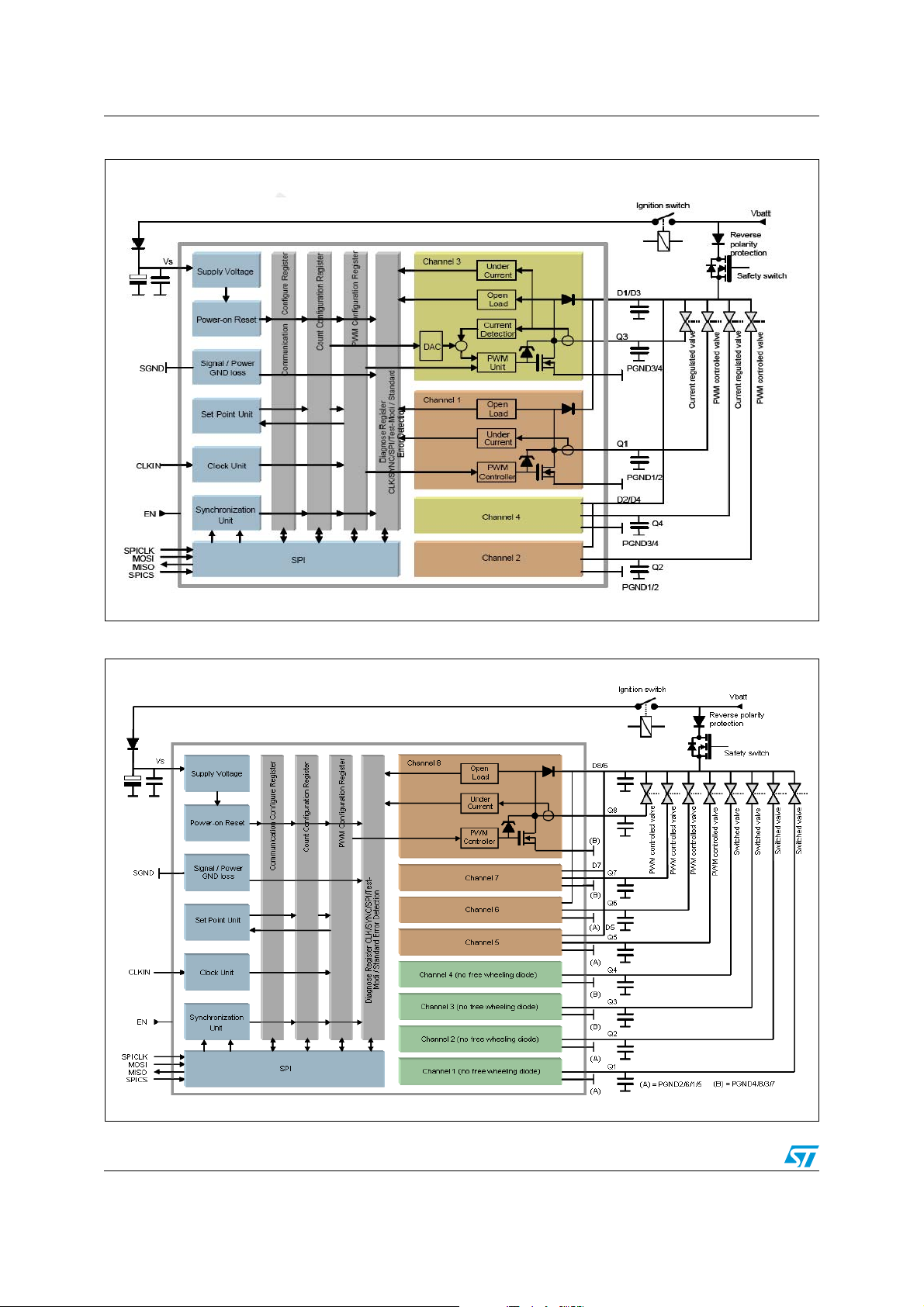
1 L9374 and L9375 summary description
The L9374 is a smart quad low side driver with integrated free-wheeling diodes (see block
diagram in figure 1). The switching of the channels is programmable via SPI (Serial
Peripheral Interface). The main time base is given by an external clock via CLKin. The Clock
Unit monitors this external clock and provides the system clock for all timings. A
Synchronization Unit is used to monitor the SPI communication and provides a sync signal
for the channel activation. The Output Duty Cycle for each channel can be programmed
individually and will be activated by the Set Point Unit. Is possible to program two output
Duty Cycles per channel with a block of 16 SPI commands as well as an individual Duration
Time for each channel actuation. The PWM Controller translates the programmed digital
duty cycle value in a PWM signal which controls the output. For the current regulated
channels the target current value is programmed. It is also possible to program two different
target currents. The target current is compared with the real load current. The output duty
cycle is then calculated with an ALU. As base for the calculation a load model is used to take
into account the variation of the real load versus the load assumption done into the first SPI
transfers setting properly the command register of address 15 (see configuration register 3).
Moreover, the L9374 ALU exploits respectively:
● measurement of the supply voltage (see VD status register of address 5);
● measurement of the voltage drop on the free-wheeling diode (see V_FWD status
register of address 10);
● measurement of the sense resistor (see Rs status register of address 11) used to
monitor the current on the Q3 and Q4 channels for the current control loop of the
L9374.
All channels are equipped with a load Diagnostic. This allows to detect an open load in off
condition as well as an under current in on condition. The power stage is protected against
over current and over temperature. A weak connection in power ground or in the
recirculation path is monitored. All monitored functions can be read out in a serial diagnostic
protocol dedicated for each channel via SPI.
The L9375 is an octal low side driver with integrated recirculation diodes for PWM controlled
channels, that is, Q5, Q6, Q7 and Q8. On the other hand, the channels Q1, Q2, Q3 and Q4
are configured as switching channels (see figure 2). To achieve a fast switch off a high
voltage output clamp is implemented for a rapid free-wheeling if the inductive load. The
switch on time can be programmed via SPI. The L9375 have the same features of the L9374
except for the current control of the channels of L9374.
5/34
Page 6
L9374 and L9375 summary description AN2804
Figure 1. L9374 application block diagram
Figure 2. L9375 application block diagram
6/34
Page 7
AN2804 VCCL: plan of accuracy evaluation
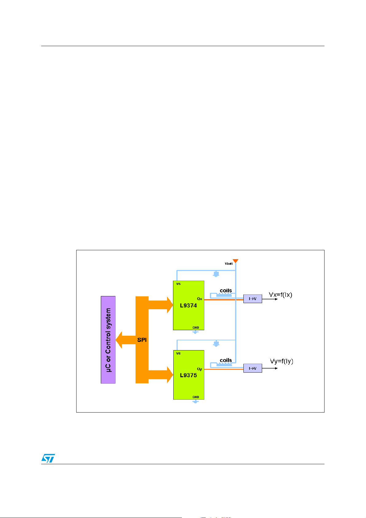
2 VCCL: plan of accuracy evaluation
The idea behind the VCCL is to use the information coming from the current feedback of the
Q3 and Q4 channels of L9374 in order to wrap the PWM channels of L9375 with a pseudo
current control loop implemented by the microcontroller of the ABS/ESC control unit. In the
Figure 3, the block diagram of the VCCL is described:
● set-up with a system microcontroller that works as the Master of the SPI
communication with the Slaves, L9374 and L9375;
● diagnostic cycle is applied to the L9374 current controlled channel (Qx), to collect all
possible information;
● diagnostic cycle is applied also to the L9375 PWM channel (Qy);
● using information from Qx and Qy diagnostic, the microcontroller calculates the duty
cycle to be imposed in order to obtain the current setpoint desired on the PWM
channels of L9375.
The target of this work is to evaluate the difference between the desired current and the
actual current (precision of the VCCL). The accuracy of the VCCL along different working
conditions have been measured by simulating different disturbances, like battery voltage
changes, load resistance change, temperature mismatches, etc.
The result of this activity is to demonstrate that it is possible to perform a low-end ABS/ESC
system with only 2 current controlled channels instead of 6 required in the conventional
system partitioning of the ABS/ESC control unit.
Figure 3. Block diagram of the VCCL
Figures 4 and 5 describe some details regarding the implementation of the evaluation plan
conceived to quantify the VCCL accuracy. First of all, after the power-up of the
microcontroller and of the L9374-L9375, a spot calibration on the Q3 channel of L9374 is
7/34
Page 8
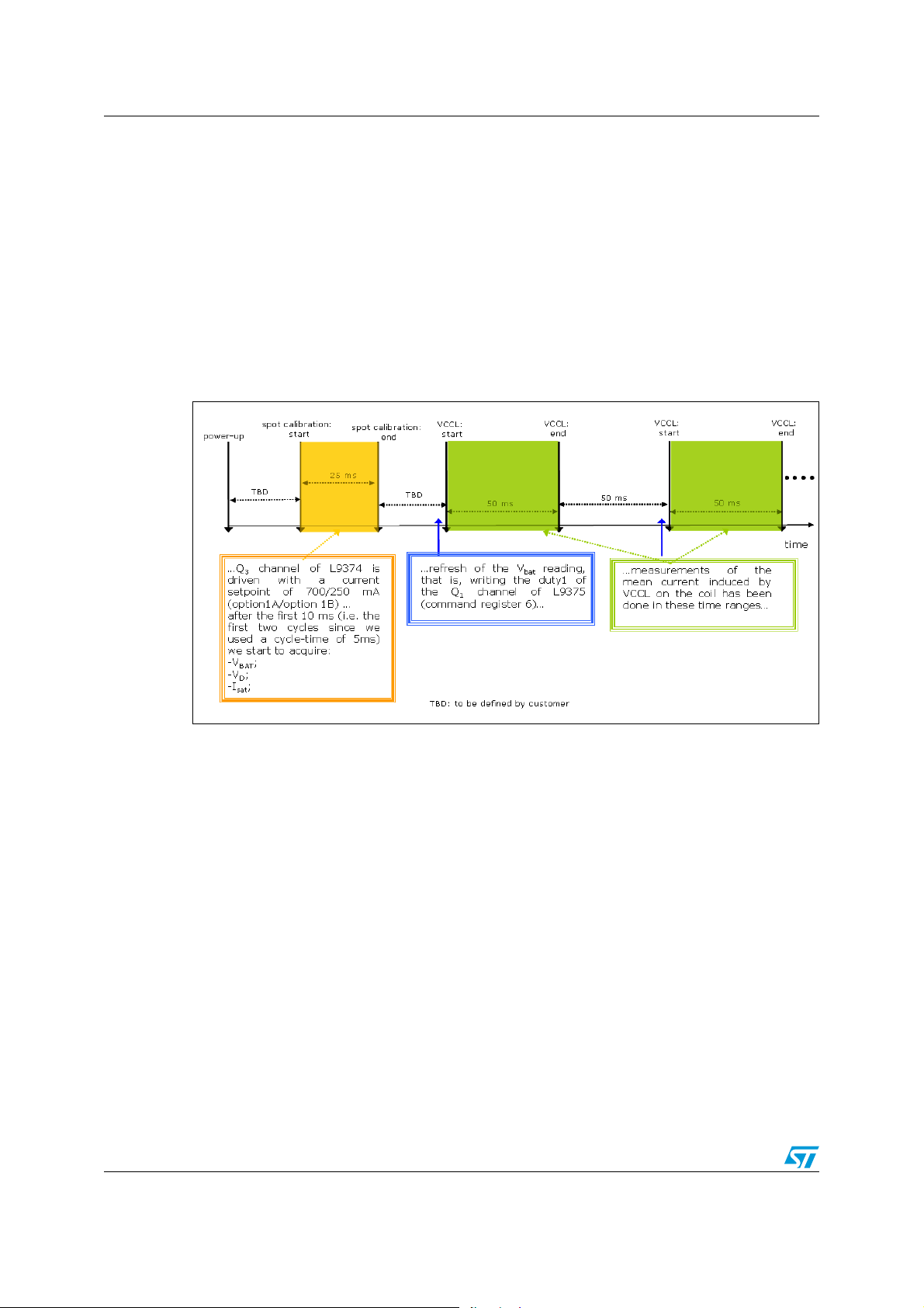
VCCL: plan of accuracy evaluation AN2804
done for about 25 ms. During this time, the Q3 channel is driven in order to energize the
corresponding coil mounted on the INLET valve head of the hydraulic modulator used in our
tests. Two current setpoints have been explored for the spot calibration on Q3 channel: 700
mA (option 1A) and 250 mA (option 1B). While the first current setpoint is enough to close
the INLET valve the last isn't. Therefore, the option 1A shows as drawback the need to close
the INLET valve linked to the Q3 channel of L9374 for the spot calibration time. We chose a
spot calibration time of 25 ms because this represents an optimal trade-off, taking into
account the test operative conditions (the cycle-time used is about 5 ms), the filter time for
the CNR condition of the current regulated channels of L9374 (t
is equal to 8 ms) and
CNR
the possibility to wait for a long enough transition time before to start the reading, by MISO
bus of SPI, the VBAT (VD status register), VD (V_FWD status register) and ISAT (ISAT_Qx
status registers) values (see Figure 5).
Figure 4. Details on the implementation of the VCCL accuracy evaluation plan
An internal common used ALU is devoted to guarantee, through the calculation of the
formula (1), the desired accuracy (6% of error against the current setpoint) for the current
control loop of the Q3 and Q4 channels of L9374. The formula (1) implemented in the ALU
takes into account a dedicated load model. This model includes the recirculation path as
well as the resistive value of the load. This value is programmable via SPI (see R
the parameters of the recirculation path and the supply voltage of the load are measured
(see Rs, V
Equation 1
, V
D
). All these values are readable via SPI.
BAT
dc
V
DITARGET
--------------------------------------------------------------------------------------------------------------------------=
V
DVBATITARGET
Rs I
The value of the programmed load (i.e. R
correction value is available via SPI (see I
can be achieved. Starting at time zero a load error is corrected by modifying the
programmed load resistor value with an integrated correction factor I
load model correction is only available for target currents higher than 110mA. In the formula
(1) the factor R
LSPI (ISAT
+ 1) represents, in a first approximation, the real load seen by the
Qx channel of L9374 into the current control loop. Anyway, for a more detailed explanation of
the current control loop of the L9374 we remand to the L9374 datasheet.
8/34
TARGETRLSPIISAT
1+()++
Rs Rds on()–()++
) is corrected during the control loop. This
LSPI
). With this algorithm a fast controller dynamic
SAT
. This function of
SAT
LSPI
) while
Page 9
AN2804 VCCL: plan of accuracy evaluation
ˆ
ˆ
ˆ
ˆ
ˆ
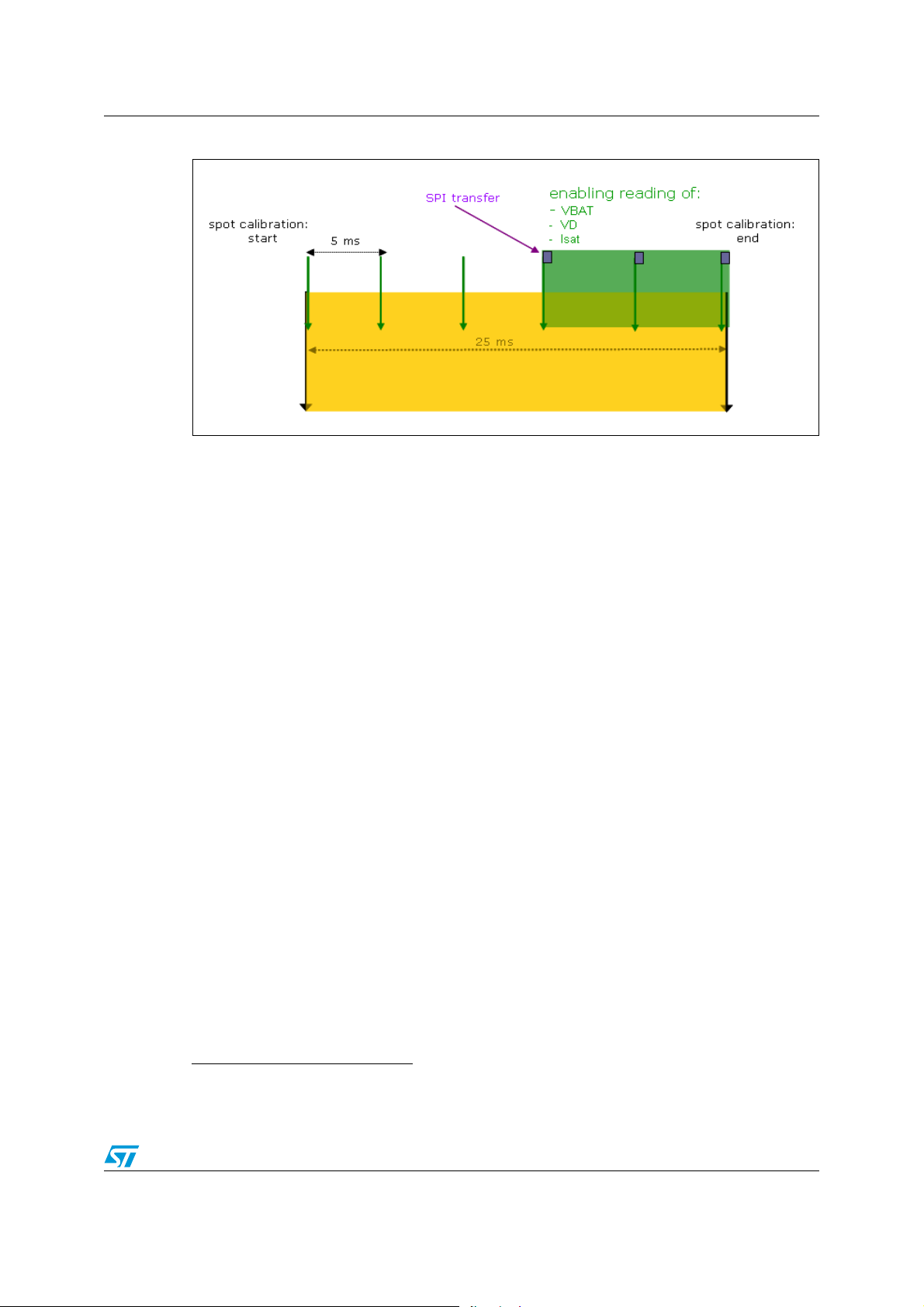
Figure 5. Details on the spot calibration of the VCCL accuracy evaluation plan
During the spot calibration, once the reading window is opened (see Figure 5), the values of
VD, VBAT, ISAT are acquired. These values after an arithmetic mean are stored in some
registers of the microcontroller. Care is taken for the ISAT value because it is represented as
a two complement number (see L9374 datasheet). The values
V
V
,,
D
BAT
I
SAT
(a)
, are used
into the formula (2) implemented by the system microcontroller in order to calculate, before
to energize the coil, the right duty cycle to have a pseudo current control loop on the PWM
channels of L9375. Since the L9375 does not have a real current control loop, in the formula
(2)) there is not the Rs resistor that we can find in the formula (1) implemented by the ALU of
L9374. However, we thought to consider a minimum resistor of 50mΩ. Furthermore, the
values of the voltage drop on the free-wheeling diode (i.e. V
) have been scaled in order to
D
maintain a ratio of 3/4 between the voltage drop on the free-wheeling diode of the PWM
channels of L9375 and the voltage drop on the free-wheeling diode of the current controlled
channels of L9374.
V
Equation 2
dc
-----------------------------------------------------------------------------------------------------------------------------------=
D
I
TARGET
ˆ
V
D
ˆ
V
BAT
50m Ω I
ˆ
I
TARGET
TARGETRLSPI
50mΩ 200mΩ–()++
I
SAT
1+()++
a. The hat on the variables indicates that they are the result of an arithmetic mean applied on the different values
read via SPI once the reading window is opened (see figure5).
9/34
Page 10
ABS/ESC: load analysis AN2804
3 ABS/ESC: load analysis
In order to validate the VCCL approach, we used the INLET valves of the ABS/ESC 8.0
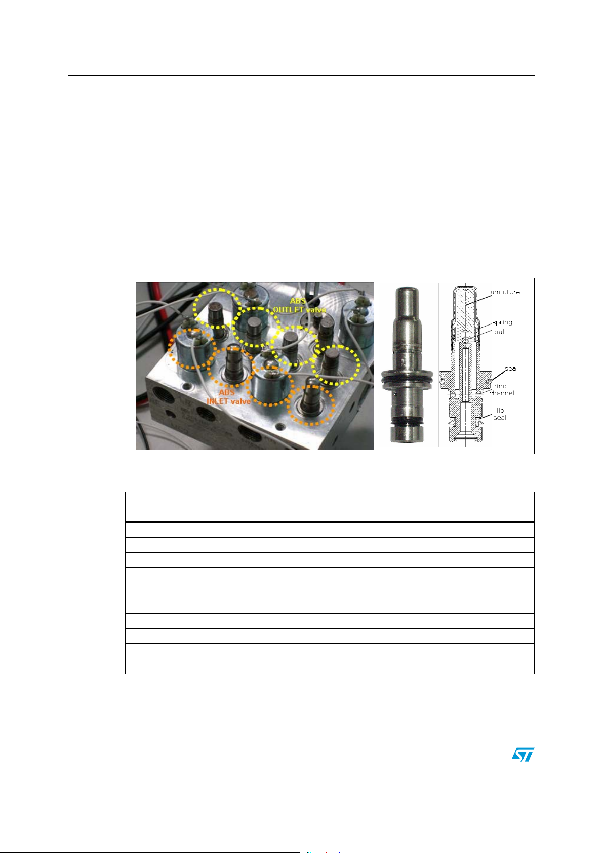
Bosch hydraulic modulator. The Figure 6 illustrates the hydraulic modulator and the section
of an INLET valve. The coil characteristics have been measured with and without the valves
by means of the Hameg LCR Meter HM8018. The obtained values are:
● R = 4.65 Ohm, L = 1.6 mH (without the valve)
● R = 5.35 Ohm, L = 7.35 mH (with the valve)
Coil characteristics have been measured, also during the calibration phase of the regulated
channel (i.e. Q3) of L9374, using the estimation of the load done by the L9374 through the
I
factor measurement.
SAT
Figure 6. ABS/ESC 8.0 Bosch Hydraulic modulator and INLET valve section
Table 1. Characterization of the load seen by the L9374 vs. the current setpoint
imposed on the Q3 channel
Regulated channel current:
setpoint (mA)
250 7.17 0.03
350 6.72 0.02
450 6.68 0.02
550 6.55 0.06
650 6.52 0.04
750 6.21 0.03
850 6.23 0.06
950 6.08 0.16
1050 5.96 0.03
1150 5.6 0.16
Load resistor seen by L9374:
The Tab l e 1 describes the results of a characterization of the load seen by the L9374 during
the spot calibration versus different current setpoints. The mean and the standard deviation
have been calculated on a set of 10 repeated measurements done in the same conditions
(supply voltage, temperature, current setpoint, etc…).
10/34
mean (Ohm)
Load resistor seen by L9374:
std (Ohm)
Page 11
AN2804 Current measurement procedure: validation
4 Current measurement procedure: validation
The test-bench layout used to measure the current is based on the following components:
● oscilloscope LeCroy wave pro 7300A in ERES (Enhanced resolution, about 211 bit of
vertical resolution) mode;
● current probe amplifier Tektronix TCPA300 (DC to 100 MHz of bandwidth, DC-gain
accuracy < 1%);
● AC/DC current probe Tektronix TCP312 (Lowest Measurable Current = 1mA, Maximum
Amp-Second = 50A*µs (for 1A/V range)).
Table 2. Characterization of the procedure used to measure the current into the
VCCL validation tests
Regulated channel
current: setpoint (mA)
250 251 1 0.4
350 352 1 0.6
450 454 1 0.9
550 557 1 1.3
650 658 1 1.2
750 755 2 0.7
850 857 2 0.8
950 958 2 0.8
1050 1057 2 0.7
1150 1157 2 0.6
1250 1252 2 0.2
1350 1344 2 -0.4
1450 1462 4 0.8
1550 1566 5 1.0
Current measured on
the Q3 of L9374: mean
(mA)
Current measured on
the Q3 of L9374: std
(mA)
Percent deviation
from the ideal current
control accuracy of
the Q3 of L9374 (%)
The Tabl e 2 shows the results obtained from a preliminary characterization of the procedure
adopted to measure the current into the VCCL validation tests. The results in the table
Tab le 2 are referred to a set of 10 repeated measurements of the current energizing the coil
during the spot calibration of the L9374 and once the reading window is opened (see
Figure 5). It is important to highlight that the measurements have been done in the same
operative conditions (supply voltage, temperature, current setpoint, etc…). From an analysis
of the results reported in theTa b l e 2 , it comes out that, in the worst case, the test bench
layout used to measure the current is reliable within the limits of the 1% of accuracy.
11/34
Page 12

VCCL accuracy evaluation AN2804
5 VCCL accuracy evaluation
The first operative conditions in which we evaluated the performance of the VCCL are the
following:
● load resistor R
● supply voltage at 12 Volt both in the calibration and actuation phases;
● ideal setpoint on the Q5 channel of L9375 in [250,1550] mA;
● current setpoint on the calibration phase at 700 mA;
● 10 repeated measurements of the current mean value on the Q5 channel of L9375
after the VCCL regulation have been acquired.
Table 3. VCCL accuracy evaluation with a spot calibration having a current
setpoint on the Q3 channel of L9374 equal to 700 mA
set to 4.375 Ohm;
LSPI
Regulated channel
current: setpoint (mA)
250 244 4 -2.3
350 343 1 -2
450 452 3 0.3
550 530 4 -3.7
650 635 5 -2.2
750 736 8 -1.9
850 844 3 -0.7
950 936 5 -1.4
1050 1022 8 -2.7
1150 1136 15 -1.2
1250 1257 8 0.5
1350 1360 14 0.7
1450 1472 23 1.5
1550 1572 14 1.4
Current measured on
the Q3 of L9374: mean
(mA)
Current measured on
the Q3 of L9374: std
(mA)
Percent deviation
from the ideal current
control accuracy of
the Q3 of L9374 (%)
12/34
Page 13

AN2804 VCCL accuracy evaluation
Figure 7. VCCL accuracy evaluation with a spot calibration having a current
setpoint on the Q3 channel of L9374 equal to 700 mA
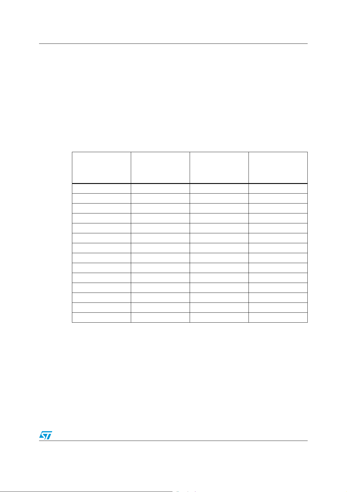
Moreover, we tested the sensitivity of the VCCL approach in the spot calibration option 1A
against power supply change. In other words, we explored the working of the VCCL when
there is a mismatch between the power supply value during the spot calibration time and
during the actuation phase of the VCCL on the PWM channels of L9375. The Tab l e 4 and
the figures 8, 9, 10 show the results of this analysis. It comes out when there is a voltage
drop going from the spot calibration on Q3 channel of L9374 to the actuation on the PWM
channels of L9375, the performance of VCCL seem to be less satisfactory than the
performance in "ideal" conditions shown before (see Ta bl e 3 and Figure 7) and the
performance when there is a voltage increase going from the spot calibration to the
actuation phase. Anyway, discarding the results referred to the ideal current setpoint of 1350
mA, also in these operative conditions, that is, voltage drop going from the spot calibration to
the actuation phase, the VCCL performance are within the 6% accuracy cone of the current
controlled channels of L9374 (see figures 8, 9, 10).
13/34
Page 14

VCCL accuracy evaluation AN2804
The Tabl e 4 shows the VCCL accuracy evaluation in option 1A spot calibration versus power
supply mismatch between the power supply value during the spot calibration time and
during the actuation phase of the VCCL on the PWM channels of L9375.
Table 4. VCCL accuracy evaluation in option 1A spot calibration versus power supply
Ideal
current
setpoint
on Q5
channel
of L9375
(mA)
250 266 6.4 254 1.6 252 0.8 247 -1.2 260 4 265 6
350 366 4.6 349 -0.3 334 -4.6 344 -1.7 366 4.6 375 7.1
450 436 -3.1 442 -1.8 435 -3.3 441 -2 448 -0.4 467 3.8
550 571 3.8 544 -1.1 550 0 525 -4.5 567 3.1 580 5.5
650 672 3.4 661 1.7 672 3.4 687 5.7 650 0 685 5.4
750 791 5.5 747 -0.4 754 0.5 746 -0.5 771 2.8 799 6.5
850 899 5.8 860 1.2 843 -0.8 849 -0.1 895 5.3 903 6.2
950 1000 5.3 955 0.5 939 -1.2 948 -0.2 988 4 998 5.1
1050 1073 2.2 1069 1.8 1032 -1.7 1074 2.3 1085 3.3 1128 7.4
1150 1211 5.3 1163 1.1 1183 2.9 1158 0.7 1193 3.7 1232 7.1
1250 1326 6.1 1266 1.3 1266 1.3 1241 -0.7 1302 4.2 1331 6.5
1350 1488 10.2 1407 4.2 1444 7 1384 2.5 1482 9.8 1513 12.1
1450 1534 5.8 1481 2.1 1439 -0.8 1444 -0.4 1524 5.1 1547 6.7
1550 1662 7.2 1610 3.9 1597 3 1568 1.2 1702 9.8 1675 8.1
12 V in cal. phase
9 V in actuation:
mean
current
on Q5 of
L9375
(mA)
percent
deviation
vs.
setpoint
(%)
12 V in cal. phase
15 V in actuation:
mean
current
on Q5 of
L9375
(mA)
percent
deviation
vs.
setpoint
(%)
9 V in cal. phase
12 V in actuation:
(mA)
percent
deviation
vs.
setpoint
(%)
mean
current
on Q5 of
L9375
9 V in cal. phase
15 V in actuation:
(mA)
percent
deviation
vs.
setpoint
(%)
mean
current
on Q5 of
L9375
15 V in cal. phase
15 V in actuation:
mean
current
on Q5 of
L9375
(mA)
percent
deviation
vs.
setpoint
(%)
15 V in cal. phase
9 V in actuation:
mean
current
on Q5 of
L9375
(mA)
percent
deviation
vs.
setpoint
(%)
14/34
Page 15
AN2804 VCCL accuracy evaluation
The Figure 8 shows VCCL accuracy evaluation in option 1A spot calibration versus power
supply mismatch between the power supply value during the spot calibration time and
during the actuation phase of the VCCL on the PWM channels of L9375.
Figure 8. VCCL accuracy evaluation in option 1A spot calibration versus power
supply
The Figure 9 shows the detail of the VCCL accuracy evaluation in option 1A spot calibration
versus power supply mismatch between the power supply value during the spot calibration
time and during the actuation phase of the VCCL on the PWM channels of L9375.
Figure 9. Detail of the VCCL accuracy evaluation in option 1A spot calibration
versus power supply
15/34
Page 16

VCCL accuracy evaluation AN2804
The Figure 10 shows the detail of the VCCL accuracy evaluation in option 1A spot
calibration versus power supply mismatch between the power supply value during the spot
calibration time and during the actuation phase of the VCCL on the PWM channels of
L9375.
Figure 10. Detail of the VCCL accuracy evaluation in option 1A spot calibration
versus power supply
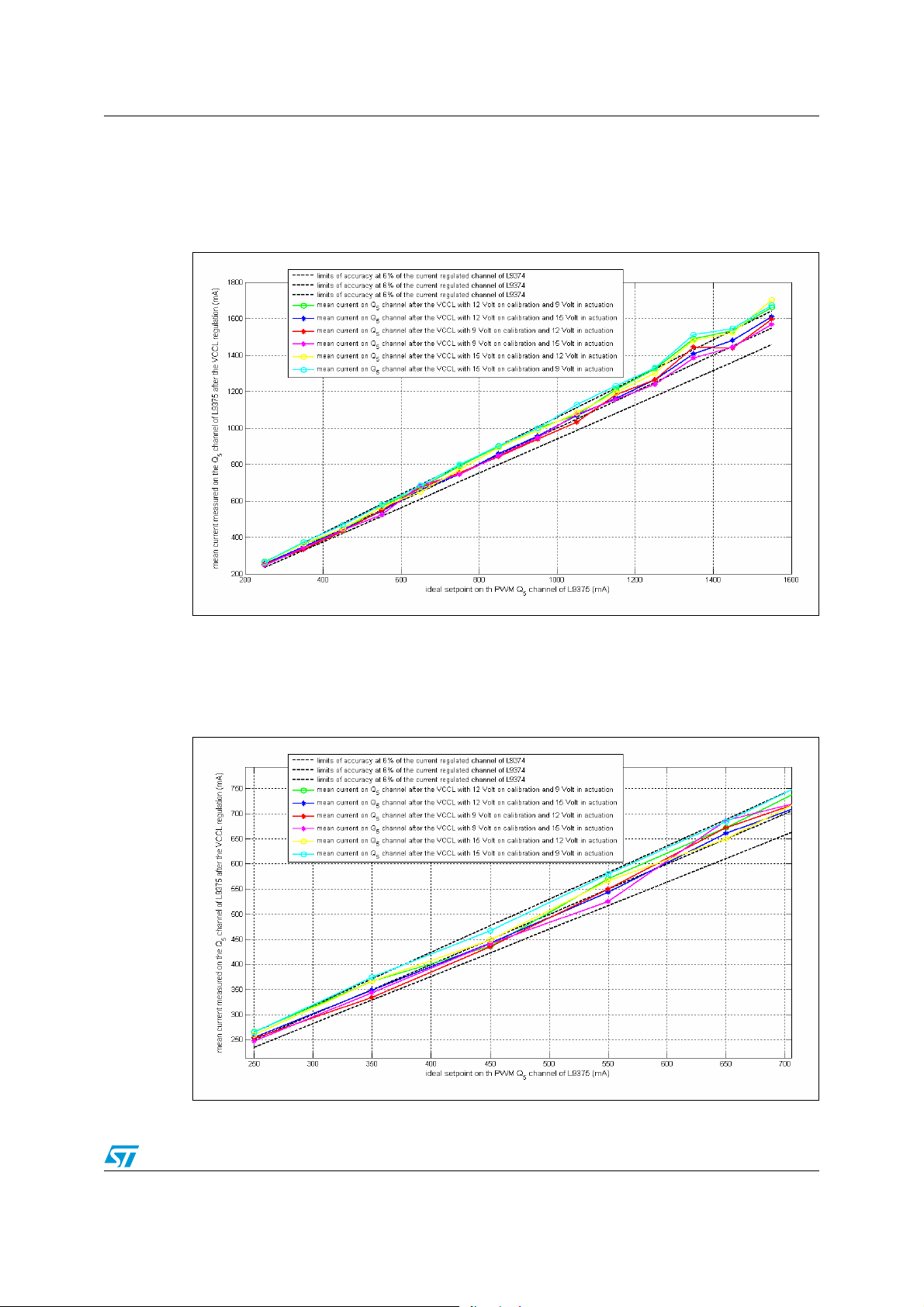
The second operative conditions in which we evaluated the performance of the VCCL are
the following:
● load resistor RLSPI set to 4.375 Ohm;
● supply voltage at 12 Volt both in the calibration and actuation phases;
● ideal setpoint on the Q5 channel of L9375 in [250,1550] mA;
● current setpoint on the calibration phase at 250 mA;
● 10 repeated measurements of the current mean value on the Q5 channel of L9375
after the VCCL regulation have been acquired.
Also in this case we analyzed the sensitivity of the VCCL approach against power supply
mismatches. In order to improve the VCCL performance we implemented a load change
model inspired to the load characterization shown in the Section 5. Basically, if this load
change model is not implemented the performance of the VCCL approach, in the calibration
option 1B, are less satisfactory than the VCCL performance obtained with the option 1A.
The main advantage of the VCCL option 1B approach is that the current required during the
spot calibration is not enough to close the INLET valve. So the customer could repeat
periodically the same calibration procedure also taking into account to change the current
setpoint of the spot calibration always keeping the current value under the minimum value
that is enough to close the INLET valve (e.g. 500-550mA mA for the INLET valve of the 8.0
Bosch ABS/ESC control unit hydraulic modulator).
16/34
Page 17

AN2804 VCCL accuracy evaluation
Table 5. VCCL accuracy evaluation with a spot calibration having a current
setpoint on the Q3 channel of L9374 equal to 250 mA
Ideal current setpoint
on Q5 channel of
L9375 (mA)
250 248 2 -0.8
350 356 4 1.7
450 447 7 -0.7
550 549 4 -0.2
650 654 7 0.6
750 749 9 -0.1
850 846 7 -0.5
950 954 6 0.4
1050 1058 2 0.8
1150 1159 11 0.8
1250 1267 12 1.4
1350 1370 10 1.5
1450 1442 13 -0.6
1550 1540 6 -0.6
Current measured on
the Q5 of L9375: mean
(mA)
Current measured on
the Q5 of L9375: std
(mA)
Percent deviation
from the ideal current
setpoint on Q5
channel of L9375 (%)
Figure 11. VCCL accuracy evaluation with a spot calibration having a current
setpoint on the Q3 channel of L9374 equal to 250 mA
The Tab le 5 and the related Figure 11 describe the behavior of the VVCL approach in the
spot calibration option 1B. On the other hand, the Tab l e 6 and the figures 12, 13, 14 show
the results of the sensitivity analysis of the approach against power supply mismatches
17/34
Page 18

VCCL accuracy evaluation AN2804
between the power supply values during the spot calibration and during the actuation phase.
Also in this case, it comes out when there is a voltage drop going from the calibration phase
to the actuation phase, the performance of the VCCL approach decreases. Anyway,
discarding the results referred to some ideal current setpoints, also in these operative
conditions, that is, voltage drop going from the spot calibration to the actuation phase, the
VCCL shows performance that are basically within the 6% accuracy cone of the current
controlled channels of L9374 (see figures 8, 9, 10).
At last, we have simulated a temperature mismatch between the coil associated to the Q3
channel of L9374 and the coil associated to the Q5 channel of L9375. Using some 30W 0.05
Ohm 1% precision resistors, we added a resistor of 0.4 Ohm in series either at the load coil
corresponding to the PWM channel of L9375 or at the load coil corresponding to the Q3
channel of L9374. Taking into account the formula (3) of the resistance of the chopper
versus the temperature and the initial value of the load resistor R
= 4.65 Ohm (see
initial
Section 5 ), it is simple to verify that the resistor of 0.4 Ohm in series corresponds to a
simulation of temperature gradient of 20°.
Equation 3
R
last
R
initial
10.004TΔ+()=
The tables 7, 8, 9, 10 and the figures 15, 16 show the results of this analysis. Also in this
case, it comes out that the accuracy of the VCCL maintains itself within the 6% accuracy
cone of the current controlled channels of L9374.
18/34
Page 19

AN2804 VCCL accuracy evaluation
The Tab le 6 shows VCCL accuracy evaluation in option 1B spot calibration versus power
supply mismatch between the power supply value during the spot calibration time and
during the actuation phase of the VCCL on the PWM channels of L9375.
Table 6. VCCL accuracy evaluation in option 1B spot calibration versus power supply
Ideal
current
setpoint
on Q5
channel
of L9375
(mA)
250 262 4.8 253 1.2 250 0 253 1.2 229 -8.4 268 7.2
350 378 8 367 4.9 368 5.1 365 4.3 377 7.7 392 12
450 466 3.6 451 0.2 449 -0.2 457 1.6 467 3.8 462 2.7
550 587 6.7 554 0.7 561 2 549 -0.2 571 3.8 588 6.9
650 691 6.3 661 1.7 653 0.5 657 1.1 679 4.5 710 9.2
750 809 7.9 772 2.9 777 3.6 764 1.9 809 7.9 811 8.1
850 928 9.2 883 3.9 854 0.5 871 2.5 873 2.7 921 8.4
950 1024 7.8 982 3.4 970 2.1 946 -0.4 1000 5.3 998 5.1
1050 1107 5.4 1052 0.2 1059 0.9 1059 0.9 1096 4.4 1124 7
1150 1205 4.8 1133 -1.5 1160 0.9 1154 0.3 1187 3.2 1220 6.1
1250 1316 5.3 1273 1.8 1253 0.2 1230 -1.6 1293 3.4 1337 7
1350 1457 7.9 1377 2 1388 2.8 1367 1.3 1453 7.6 1524 12.9
1450 1484 2.3 1426 -1.7 1442 -0.6 1420 -2.1 1467 1.2 1516 4.6
1550 1628 5 1578 1.8 1594 2.8 1581 2 1607 3.7 1645 6.1
12 V in cal. phase
9 V in actuation:
mean
current
on Q5 of
L9375
(mA)
percent
deviation
vs.
setpoint
(%)
12 V in cal. phase
15 V in actuation:
mean
current
on Q5 of
L9375
(mA)
percent
deviation
vs.
setpoint
(%)
9 V in cal. phase
12 V in actuation:
(mA)
percent
deviation
vs.
setpoint
(%)
mean
current
on Q5 of
L9375
9 V in cal. phase
15 V in actuation:
mean
current
on Q5 of
L9375
(mA)
percent
deviation
vs.
setpoint
(%)
15 V in cal. phase
15 V in actuation:
mean
current
on Q5 of
L9375
(mA)
percent
deviation
vs.
setpoint
(%)
15 V in cal. phase
9 V in actuation:
mean
current
on Q5 of
L9375
(mA)
percent
deviation
vs.
setpoint
(%)
19/34
Page 20

VCCL accuracy evaluation AN2804
The Figure 12 shows VCCL accuracy evaluation in option 1B spot calibration versus power
supply mismatch between the power supply value during the spot calibration time and
during the actuation phase of the VCCL on the PWM channels of L9375.
Figure 12. VCCL accuracy evaluation in option 1B spot calibration versus power
supply
The Figure 13 shows the detail of the VCCL accuracy evaluation in option 1B spot
calibration versus power supply mismatch between the power supply value during the spot
calibration time and during the actuation phase of the VCCL on the PWM channels of
L9375.
Figure 13. Detail of the VCCL accuracy evaluation in option 1B spot calibration
versus power supply
20/34
Page 21

AN2804 VCCL accuracy evaluation
The Figure 14 shows the detail of the VCCL accuracy evaluation in option 1B spot
calibration versus power supply mismatch between the power supply value during the spot
calibration time and during the actuation phase of the VCCL on the PWM channels of
L9375.
Figure 14. Detail of the VCCL accuracy evaluation in option 1B spot calibration
versus power supply
The Tab le 7 shows the VCCL accuracy evaluation in option 1A when a temperature
mismatch of 20° is simulated. A precision resistor of 0.4 Ohm is added in series at the coil
corresponding to the Q5 channel of L9375.
Table 7. VCCL accuracy evaluation in option 1A when a temperature mismatch of
20° is simulated (Q5 channel of L9375)
Ideal setpoint (mA) Mean (mA)
250 240 -4
350 347 -0.9
450 431 -4.2
550 527 -4.2
650 627 -3.5
750 721 -3.9
850 828 -2.6
950 999 5.2
1050 1004 -4.4
1150 1094 -4.9
1250 1202 -3.8
1350 1341 -0.7
1450 1408 -2.9
1550 1530 -1.3
Max percent error measured on the Q5
channel of L9375 after the VCCL (%)
21/34
Page 22

VCCL accuracy evaluation AN2804
The Tab le 8 shows the VCCL accuracy evaluation in option 1A when a temperature
mismatch of 20° is simulated. A precision resistor of 0.4 Ohm is added in series at the coil
corresponding to the Q3 channel of L9374.
Table 8. VCCL accuracy evaluation in option 1A when a temperature mismatch of
20° is simulated (Q3 channel of L9375)
Ideal setpoint (mA) Mean (mA)
250 248 -0.8
350 346 -1.1
450 423 -6
550 520 -5.5
650 650 0
750 747 -0.4
850 855 0.6
950 971 2.2
1050 1053 0.3
1150 1165 1.3
1250 1274 1.9
1350 1404 4
1450 1507 3.9
1550 1622 4.6
Max percent error measured on the Q5
channel of L9375 after the VCCL (%)
The Tab le 9 shows the VCCL accuracy evaluation in option 1B when a temperature
mismatch of 20° is simulated. A precision resistor of 0.4 Ohm is added in series at the coil
corresponding to the Q5 channel of L9375.
Table 9. VCCL accuracy evaluation in option 1B when a temperature mismatch of
20° is simulated (Q5 channel of L9375)
Ideal setpoint (mA) Mean (mA)
250 254 1.7
350 358 2.4
450 442 -1.8
550 549 -0.2
650 633 -2.6
750 746 -0.5
850 845 -0.6
950 937 -1.4
1050 1032 -1.7
1150 1132 -1.6
1250 1249 -0.1
1350 1365 1.1
1450 1442 -0.6
1550 1550 0
Max percent error measured on the Q5
channel of L9375 after the VCCL (%)
22/34
Page 23
AN2804 VCCL accuracy evaluation
TheTab le 1 0 shows the VCCL accuracy evaluation in option 1B when a temperature
mismatch of 20° is simulated. A precision resistor of 0.4 Ohm is added in series at the coil
corresponding to the Q3 channel of L9374.
Table 10. VCCL accuracy evaluation in option 1B when a temperature mismatch of
20° is simulated (Q3 channel of L9375)
Ideal setpoint (mA) Mean (mA)
250 256 2.4
350 367 4.9
450 462 2.7
550 573 4.2
650 679 4.5
750 778 3.7
850 885 4.1
950 994 4.6
1050 1092 4
1150 1218 5.9
1250 1316 5.3
1350 1469 8.8
1450 1475 1.7
1550 1628 5
Max percent error measured on the Q5
channel of L9375 after the VCCL (%)
The Figure 15 shows the sensitivity versus coil temperature in the option 1A VCCL, results
with a mismatch of 0.4 Ohm between the load resistor of the Q3 channel of L9374 and the
Q5 channel of L9375
Figure 15. Sensitivity versus coil temperature in the option 1A VCCL
23/34
Page 24

VCCL accuracy evaluation AN2804
The Figure 16 shows the sensitivity versus coil temperature in the option 1B VCCL, results
with a mismatch of 0.4 Ohm between the load resistor of the Q3 channel of L9374 and the
Q5 channel of L9375
Figure 16. Sensitivity versus coil temperature in the option 1B VCCL
24/34
Page 25

AN2804 VCCL: computational burden evaluation
6 VCCL: computational burden evaluation
The Figure 17 describes, in a more detail, the implementation of the VCCL. During the spot
calibration once there is the enabling of the reading window (see Figure 5), the values of VD,
VBAT, ISAT are acquired. Before to start the actuation on the Q5 channel of L9375, we
update the reading of the VBAT by means of the setting of the command register 6 of the
L9375, that is, we set the duty1 of the Q1 channel of L9375. These values are stored and
averaged. The arithmetic means are the inputs of the main function of the VCCL:
VCCL_dc_calculation. This function calculates the duty-cycle value according to the formula
(2). This duty-cycle value is used to set the command registers of the Q5 channel of L9375
in order to carry out the VCCL.
From a point of view of the computation load, we analyzed the cost of the
VCCL_dc_calculation function call for two different microcontroller architectures
(ST10F252M and ST-Pictus) by two different approaches:
● Toggling a pin before and after the VCCL_dc_calculation function call;
● Counting the number of instruction-cycles.
Figure 17. Details on the implementation of the VCCL
Toggling a pin before and after the VCCL_dc_calculation function call, we observed that the
cost of the VCCL_dc_calculation function call is 27µs for the ST10F252M and 4 µs for the
ST-Pictus, respectively. Moreover, counting the number of instruction-cycles, we estimated
about 500 instruction-cycle for each VCCL_dc_calculation function call on a microcontroller
architecture similar to ST10 one and we estimated about 250 instruction-cycle for each
VCCL_dc_calculation function call on a microcontroller architecture similar to ST-Pictus one.
Considering that for the ST10 microcontroller architecture there is a correspondence of 2
clock-hits for each instruction-cycle, the VCCL_dc_calculation function call costs about 1000
25/34
Page 26

VCCL: computational burden evaluation AN2804
clock-hits, that is, about 25 µs for the ST10F252M clock-frequency at 40 MHz. On the other
hand, considering that for ST-Pictus microcontroller architecture there is a correspondence
of 1 clock-hit for each instruction-cycle, the VCCL_dc_calculation function call costs about
250 clock-hit, that is, about 3.9 µs for the clock-frequency at 64 MHz. Both the estimation
based on the counting of the instruction-cycles number confirm the results measured by the
oscilloscope via toggling mode approach. Finally, taking into account that the worst case is
when you have to drive all the 4 PWM channels of the L9375 setting two different duty-cycle
values (two different current set-points) into the cycle-time, this means 8 different
VCCL_dc_calculation function calls for each cycle-time, that is, about 200 µs for the
STF252M and 32 µs for the ST-Pictus, respectively.
26/34
Page 27
AN2804 VCCL: fixed point arithmetic
ˆ
ˆ
ˆ
ˆ
ˆ
7 VCCL: fixed point arithmetic
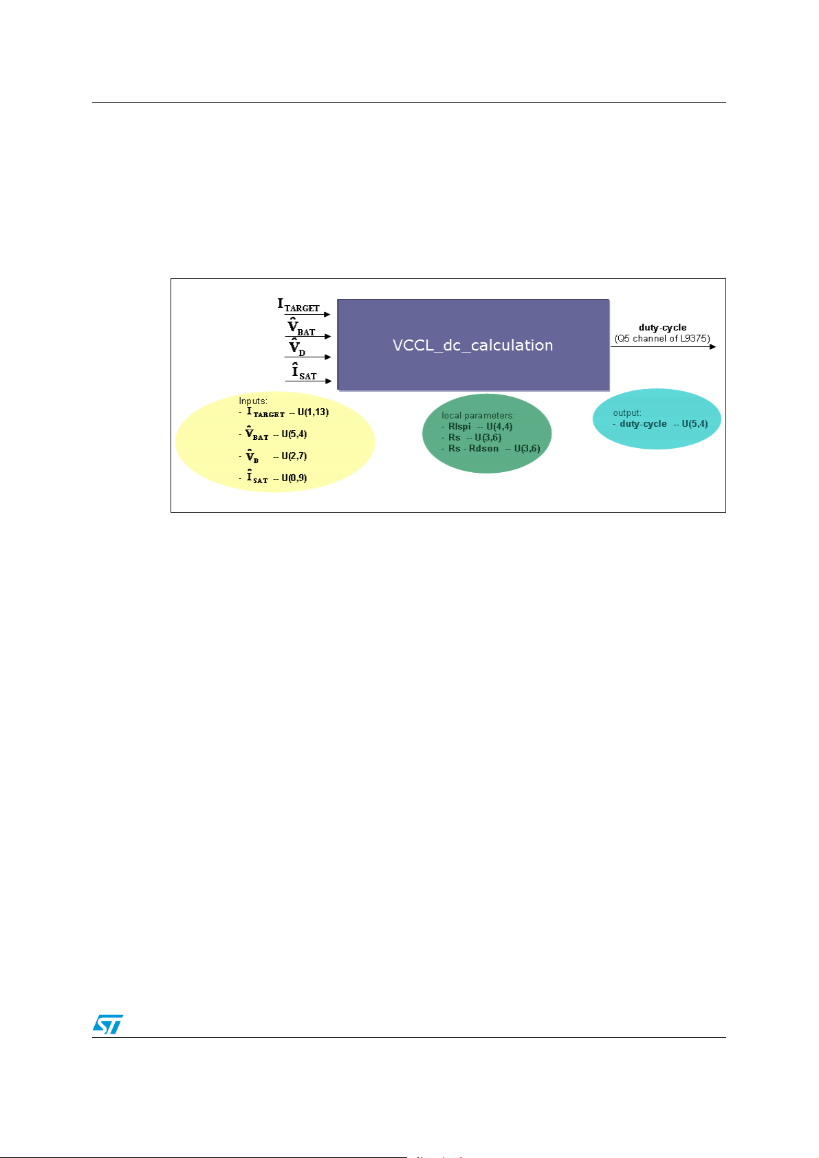
The Figure 18 describes the implementation of the VCCL_dc_calculation function. The
averaged values of with the current setpoint I
VCCL_dc_calculation function. The local parameters Rs and Rdson are equal to 50 mΩ and
200 mΩ, respectively.
Figure 18. Details on the implementation of the VCCL_dc_calculation function
V
V
,,
D
BAT
I
SAT
TA R GE T
are the inputs of the
The inputs, outputs and the local parameters of the VCCL_dc_calculation function are
interpreted as unsigned fixed point rationals. Even though, is represented on the
I
SAT
status registers 8 and 9 of the L9374 as a two complement number, for a sake of simplicity,
we preferred to consider as an U(0,9) number. If the sign bit, the MSB of the data bits
I
SAT
string is low I read the least significant 9 bits as an U(0,9), otherwise if the sign bit if the sign
bit is high I read the least significant 9 bits as an U(0,9) after a not of the word plus 1.
Furthermore, I read I
TA R GE T
interpretation of the current setpoint (i.e. I
as an U(1,13). It is possible to demonstrate that this
TA R GE T
) implies an error in data representation of
0.5%.
The steps of the VCCL_dc_calculation function call are the following:
● (1+I
● I
● I
● Num1 = I
● Num2 = (Rlspi*(1+Isat))>>2 - U(5,11)
● Num2 = I
● NumEff = Num1 + Num2>>7 -- U(7,17)
● Den1 = Vd + Vbat<<3 -- U(6,7)
● Den2 = I
● DenEff = Den1<<6 + Den2>>6 - U(7,13)
● NumEff = NumEff>>4 -- U(7,13)
● NumEff = NumEff*100
● dc = (NumEff<<4)/DenEff … I read this as an U(5,4)
sat
TA RG E T
TA RG E T
) - U(1,9)
*Rs - U(4,19)
*Rs>>2 - U(4,17)
TA R GE T
TA R GE T
TA RG E T
*Rs + Vd<<10 -- U(5,17)
*Rlspi*(1+Isat) - U(6,24)
*(Rs-Rsdson) -- U(4,19)
27/34
Page 28

VCCL: fixed point arithmetic AN2804
The local variables listed before are unsigned integer at 32 bits. After the duty-cycle
calculation, you have only to set the command registers (i.e. 10, 11, 12, 13) of the PWM
channels of L9375 you want to drive as there was a current control loop.
At last, we reassume, in the Ta bl e 11 , the results of an off-line characterization of the
VCCL_dc_calculation function for different values of the current setpoint and of the Isat
factor.
Table 11. Analysis of the error propagation in the VCCL_dc_calculation function
call versus different Isat value and current setpoints
Isat
value
Setpoint 250 mA
0.1 15.7 15.5 1.3
0.3 17.52 17.3125 1.2
0.5 19.355 19.1875 0.9
-0.1 13.853 13.6875 1.2
-0.3 12.02 11.81 1.7
-0.5 10.185 10 1.8
Setpoint 350 mA
0.1 19.91 19.56 1.8
0.3 22.48 22.12 1.6
0.5 25.05 24.625 1.7
-0.1 17.338 17 1.9
-0.3 14.767 14.4375 2.2
-0.5 12.196 11.9375 2.1
Setpoint 450 mA
Floating point
calculation of duty
cycle
Fixed point
calculation of duty
cycle
Percent error between
fixed and floating point
calculation
0.1 24.147 23.75 1.6
0.3 27.458 27.06 1.4
0.5 30.769 30.31 1.5
-0.1 20.835 20.4375 1.9
-0.3 17.524 17.1875 1.9
-0.5 14.213 13.875 2.4
Setpoint 550 mA
0.1 27.96 28.06 -0.4
0.3 29.98 30.06 -0.3
0.5 36.06 36.18 -0.3
-0.1 23.9 24 -0.4
28/34
Page 29

AN2804 VCCL: fixed point arithmetic
Table 11. Analysis of the error propagation in the VCCL_dc_calculation function
call versus different Isat value and current setpoints (continued)
Isat
value
-0.3 19.85 19.93 -0.4
-0.5 15.79 15.87 -0.5
Setpoint 650 mA
0.1 32.658 32.3125 1.1
0.3 37.455 37.0625 1.0
0.5 42.253 41.875 0.9
-0.1 27.861 27.5 1.3
-0.3 23.063 22.6875 1.6
-0.5 18.265 17.875 2.1
Setpoint 750 mA
0.1 36.933 36.5625 1.0
0.3 42.477 42.125 0.8
0.5 48.02 47.625 0.8
-0.1 31.389 31 1.2
-0.3 25.845 25.4375 1.6
Floating point
calculation of duty
cycle
Fixed point
calculation of duty
cycle
Percent error between
fixed and floating point
calculation
-0.5 20.3 19.875 2.1
Setpoint 850 mA
0.1 40.55 40.81 -0.6
0.3 46.85 47.12 -0.6
0.5 53.14 53.37 -0.4
-0.1 34.26 34.5 -0.7
-0.3 27.96 28.18 -0.8
-0.5 21.67 21.87 -0.9
Setpoint 950 mA
0.1 45.52 45.06 1.0
0.3 52.566 52.125 0.8
0.5 59.61 59.1875 0.7
-0.1 38.478 38 1.2
-0.3 31.434 30.9375 1.6
-0.5 24.391 23.875 2.1
Setpoint 1050 mA
0.1 49.836 49.375 0.9
29/34
Page 30

VCCL: fixed point arithmetic AN2804
Table 11. Analysis of the error propagation in the VCCL_dc_calculation function
call versus different Isat value and current setpoints (continued)
Isat
value
0.3 57.633 57.1875 0.8
0.5 65.43 65.0625 0.6
-0.1 42.04 41.5625 1.1
-0.3 34.242 33.75 1.4
-0.5 26.445 25.9375 1.9
Setpoint 1150 mA
0.1 53.22 53.68 -0.9
0.3 61.53 62.31 -1.3
0.5 70.089 70.87 -1.1
-0.1 44.67 45.125 -1.0
-0.3 36.12 36.56 -1.2
-0.5 27.57 27.93 -1.3
Setpoint 1450 mA
0.1 66.05 66.68 -1.0
0.3 76.89 77.56 -0.9
Floating point
calculation of duty
cycle
Fixed point
calculation of duty
cycle
Percent error between
fixed and floating point
calculation
0.5 87.72 88.5 -0.9
-0.1 55.22 55.81 -1.1
-0.3 44.38 44.93 -1.2
-0.5 33.55 34.06 -1.5
Setpoint 1550 mA
0.1 70.36 71.18 -1.2
0.3 81.96 82.87 -1.1
0.5 93.56 94.56 -1.1
-0.1 58.76 59.56 -1.4
-0.3 47.16 47.81 -1.4
-0.5 35.56 36.12 -1.6
Setpoint 1650 mA
0.1 74.67 75.62 -1.3
0.3 87.04 88.12 -1.2
0.5 99.41 100 -0.6
-0.1 62.31 63.18 -1.4
-0.3 49.94 50.68 -1.5
30/34
Page 31
AN2804 VCCL: fixed point arithmetic
Table 11. Analysis of the error propagation in the VCCL_dc_calculation function
call versus different Isat value and current setpoints (continued)
Isat
value
-0.5 37.57 38.25 -1.8
Setpoint 1750 mA
0.1 79.01 80.06 -1.3
0.3 92.14 93.31 -1.3
0.5 100 100 0.0
-0.1 65.87 66.87 -1.5
-0.3 52.73 53.56 -1.6
-0.5 39.59 40.31 -1.8
Floating point
calculation of duty
cycle
Fixed point
calculation of duty
cycle
Percent error between
fixed and floating point
calculation
31/34
Page 32

Acronyms AN2804
8 Acronyms
Table 12. Acronyms
Acronym Name
ABS Antilock Brake System
ALU Arithmetic Logic Unit
CNR Current Not Reachable
ESC Electronic Stability Control
ESP Electronic Stability Program
MISO Master Input Slave Output
MOSI Master Output Slave Input
PWM Pulse Width Modulation
SPI Serial Peripheral Interface
TCS Traction Control System
VCCL Virtual Current Control Loop
32/34
Page 33

AN2804 Revision history
9 Revision history
Table 13. Document revision history
Date Revision Changes
25-Jul-2008 1 Initial release.
33/34
Page 34

AN2804
Please Read Carefully:
Information in this document is provided solely in connection with ST products. STMicroelectronics NV and its subsidiaries (“ST”) reserve the
right to make changes, corrections, modifications or improvements, to this document, and the products and services described herein at any
time, without notice.
All ST products are sold pursuant to ST’s terms and conditions of sale.
Purchasers are solely responsible for the choice, selection and use of the ST products and services described herein, and ST assumes no
liability whatsoever relating to the choice, selection or use of the ST products and services described herein.
No license, express or implied, by estoppel or otherwise, to any intellectual property rights is granted under this document. If any part of this
document refers to any third party products or services it shall not be deemed a license grant by ST for the use of such third party products
or services, or any intellectual property contained therein or considered as a warranty covering the use in any manner whatsoever of such
third party products or services or any intellectual property contained therein.
UNLESS OTHERWISE SET FORTH IN ST’S TERMS AND CONDITIONS OF SALE ST DISCLAIMS ANY EXPRESS OR IMPLIED
WARRANTY WITH RESPECT TO THE USE AND/OR SALE OF ST PRODUCTS INCLUDING WITHOUT LIMITATION IMPLIED
WARRANTIES OF MERCHANTABILITY, FITNESS FOR A PARTICULAR PURPOSE (AND THEIR EQUIVALENTS UNDER THE LAWS
OF ANY JURISDICTION), OR INFRINGEMENT OF ANY PATENT, COPYRIGHT OR OTHER INTELLECTUAL PROPERTY RIGHT.
UNLESS EXPRESSLY APPROVED IN WRITING BY AN AUTHORIZED ST REPRESENTATIVE, ST PRODUCTS ARE NOT
RECOMMENDED, AUTHORIZED OR WARRANTED FOR USE IN MILITARY, AIR CRAFT, SPACE, LIFE SAVING, OR LIFE SUSTAINING
APPLICATIONS, NOR IN PRODUCTS OR SYSTEMS WHERE FAILURE OR MALFUNCTION MAY RESULT IN PERSONAL INJURY,
DEATH, OR SEVERE PROPERTY OR ENVIRONMENTAL DAMAGE. ST PRODUCTS WHICH ARE NOT SPECIFIED AS "AUTOMOTIVE
GRADE" MAY ONLY BE USED IN AUTOMOTIVE APPLICATIONS AT USER’S OWN RISK.
Resale of ST products with provisions different from the statements and/or technical features set forth in this document shall immediately void
any warranty granted by ST for the ST product or service described herein and shall not create or extend in any manner whatsoever, any
liability of ST.
ST and the ST logo are trademarks or registered trademarks of ST in various countries.
Information in this document supersedes and replaces all information previously supplied.
The ST logo is a registered trademark of STMicroelectronics. All other names are the property of their respective owners.
© 2008 STMicroelectronics - All rights reserved
STMicroelectronics group of companies
Australia - Belgium - Brazil - Canada - China - Czech Republic - Finland - France - Germany - Hong Kong - India - Israel - Italy - Japan -
Malaysia - Malta - Morocco - Singapore - Spain - Sweden - Switzerland - United Kingdom - United States of America
www.st.com
34/34
 Loading...