

Page 1

AN2800
Application note
STM8A UART emulator
Introduction
This application note describes a technique to emulate the universal asynchronous receiver
transmitter (UART) hardware peripheral, through the microcontroller medium end timer
(TIMER3), without the use of additional hardware.
TIMER3 was chosen for this purpose because its capture and compare features can be
easily used to receive and transmit data in a non return to zero (NRZ) serial format. This
timer also provides a necessary time reference to establish when to send and read each
outgoing and incoming data frame bit. In addition, TIMER3 was chosen because it has all
the necessary features to build a software UART. Features include two timer channels, one
for transmission (TIMER3_CC2) and one for reception (TIMER3_CC1). The input capture
feature of channel one allows detection of an incoming data frame start bit, whereas its
compare feature indicates when the bits have to be read. The output compare feature of
channel two allows transmission of a data frame.
The algorithm described in this document is an example which can be further customized
and improved. It is explained in Section 7: The UART emulator software algorithm on
page 14, together with information on how to configure and use a UART emulator. The
algorithm handles several UART hardware features via software such as, selection of the
operating mode, noise and frame error detection, programmable data word length and
configurable stop bit numbers.
The algorithm was tested by connecting the STM8A microcontroller to a PC through an
RS232 interface.
For further information on STM8A devices, please refer to the STM8A datasheets which are
available on st.com.
November 2008 Rev 1 1/33
www.st.com
Page 2

Contents AN2800
Contents
1 Main features of the UART emulator . . . . . . . . . . . . . . . . . . . . . . . . . . . . 6
1.1 UART emulator receiver (RX) . . . . . . . . . . . . . . . . . . . . . . . . . . . . . . . . . . . 6
1.2 UART emulator transmitter (TX) . . . . . . . . . . . . . . . . . . . . . . . . . . . . . . . . . 6
2 UART communication protocol . . . . . . . . . . . . . . . . . . . . . . . . . . . . . . . . 7
3 UART data frame description . . . . . . . . . . . . . . . . . . . . . . . . . . . . . . . . . . 8
4 Data transmission . . . . . . . . . . . . . . . . . . . . . . . . . . . . . . . . . . . . . . . . . . . 9
4.1 Configurable stop bits . . . . . . . . . . . . . . . . . . . . . . . . . . . . . . . . . . . . . . . . . 9
4.2 General procedure for sending a data word . . . . . . . . . . . . . . . . . . . . . . . . 9
4.3 Single byte transmission . . . . . . . . . . . . . . . . . . . . . . . . . . . . . . . . . . . . . 10
4.4 Consecutive byte transmissions . . . . . . . . . . . . . . . . . . . . . . . . . . . . . . . . 10
5 Data reception . . . . . . . . . . . . . . . . . . . . . . . . . . . . . . . . . . . . . . . . . . . . . 11
5.1 Receiver data register full (RDRF) . . . . . . . . . . . . . . . . . . . . . . . . . . . . . . 11
5.2 General procedure for receiving a data word . . . . . . . . . . . . . . . . . . . . . . 11
5.3 Noise error . . . . . . . . . . . . . . . . . . . . . . . . . . . . . . . . . . . . . . . . . . . . . . . . 12
5.4 Frame error . . . . . . . . . . . . . . . . . . . . . . . . . . . . . . . . . . . . . . . . . . . . . . . . 12
5.5 Configurable stop bits during reception . . . . . . . . . . . . . . . . . . . . . . . . . . 12
6 Baud rate generator . . . . . . . . . . . . . . . . . . . . . . . . . . . . . . . . . . . . . . . . 13
7 The UART emulator software algorithm . . . . . . . . . . . . . . . . . . . . . . . . 14
7.1 UART emulator software registers . . . . . . . . . . . . . . . . . . . . . . . . . . . . . . 15
7.1.1 UART_CR . . . . . . . . . . . . . . . . . . . . . . . . . . . . . . . . . . . . . . . . . . . . . . . 15
7.1.2 UART_SR . . . . . . . . . . . . . . . . . . . . . . . . . . . . . . . . . . . . . . . . . . . . . . . 16
7.1.3 Receiver_Data_Register . . . . . . . . . . . . . . . . . . . . . . . . . . . . . . . . . . . . 16
7.2 UART emulator initialization function . . . . . . . . . . . . . . . . . . . . . . . . . . . . 17
7.2.1 Transmission time line . . . . . . . . . . . . . . . . . . . . . . . . . . . . . . . . . . . . . . 19
7.3 UART emulator de-initialization functions . . . . . . . . . . . . . . . . . . . . . . . . . 21
7.3.1 Changing the operating mode: Example 1 . . . . . . . . . . . . . . . . . . . . . . 21
7.3.2 Changing the operating mode: Example 2 . . . . . . . . . . . . . . . . . . . . . . 21
2/33
Page 3

AN2800 Contents
7.4 Functional description of data transmission . . . . . . . . . . . . . . . . . . . . . . . 22
7.4.1 Sending a data frame . . . . . . . . . . . . . . . . . . . . . . . . . . . . . . . . . . . . . . 23
7.4.2 Transmitting a single data word . . . . . . . . . . . . . . . . . . . . . . . . . . . . . . . 25
7.5 Functional description of data reception . . . . . . . . . . . . . . . . . . . . . . . . . 26
8 Connecting the UART emulator to a PC . . . . . . . . . . . . . . . . . . . . . . . . 28
9 Main.c examples . . . . . . . . . . . . . . . . . . . . . . . . . . . . . . . . . . . . . . . . . . . 29
9.1 Example 1 . . . . . . . . . . . . . . . . . . . . . . . . . . . . . . . . . . . . . . . . . . . . . . . . 29
9.2 Example 2 . . . . . . . . . . . . . . . . . . . . . . . . . . . . . . . . . . . . . . . . . . . . . . . . 31
10 Revision history . . . . . . . . . . . . . . . . . . . . . . . . . . . . . . . . . . . . . . . . . . . 32
3/33
Page 4

List of tables AN2800
List of tables
Table 1. UART_CR description . . . . . . . . . . . . . . . . . . . . . . . . . . . . . . . . . . . . . . . . . . . . . . . . . . . . 15
Table 2. UART_SR description. . . . . . . . . . . . . . . . . . . . . . . . . . . . . . . . . . . . . . . . . . . . . . . . . . . . . 16
Table 3. Configuring channels 1 and 2 of timer2 . . . . . . . . . . . . . . . . . . . . . . . . . . . . . . . . . . . . . . . 18
Table 4. Bit value majority voting system . . . . . . . . . . . . . . . . . . . . . . . . . . . . . . . . . . . . . . . . . . . . . 27
Table 5. Document revision history . . . . . . . . . . . . . . . . . . . . . . . . . . . . . . . . . . . . . . . . . . . . . . . . . 32
4/33
Page 5

AN2800 List of figures
List of figures
Figure 1. Nine-bit data word with one stop bit . . . . . . . . . . . . . . . . . . . . . . . . . . . . . . . . . . . . . . . . . . . 8
Figure 2. One bit delay. . . . . . . . . . . . . . . . . . . . . . . . . . . . . . . . . . . . . . . . . . . . . . . . . . . . . . . . . . . . 19
Figure 3. Stop bit . . . . . . . . . . . . . . . . . . . . . . . . . . . . . . . . . . . . . . . . . . . . . . . . . . . . . . . . . . . . . . . . 19
Figure 4. Start bit . . . . . . . . . . . . . . . . . . . . . . . . . . . . . . . . . . . . . . . . . . . . . . . . . . . . . . . . . . . . . . . . 20
Figure 5. Two stop bits. . . . . . . . . . . . . . . . . . . . . . . . . . . . . . . . . . . . . . . . . . . . . . . . . . . . . . . . . . . . 20
Figure 6. Data frame structure . . . . . . . . . . . . . . . . . . . . . . . . . . . . . . . . . . . . . . . . . . . . . . . . . . . . . . 22
Figure 7. Reception on TIMER3_CC1 . . . . . . . . . . . . . . . . . . . . . . . . . . . . . . . . . . . . . . . . . . . . . . . . 26
Figure 8. Reading the RX line level . . . . . . . . . . . . . . . . . . . . . . . . . . . . . . . . . . . . . . . . . . . . . . . . . . 27
Figure 9. PC-ST232- STM8A system overview . . . . . . . . . . . . . . . . . . . . . . . . . . . . . . . . . . . . . . . . . 28
5/33
Page 6

Main features of the UART emulator AN2800
1 Main features of the UART emulator
The main features of the UART emulator are:
● Transmitter mode up to 28800 bits per second (bps)
● Receiver mode up to 28800 bps
● Full duplex mode up to 28800 bps
● Control and status registers
● Separate enable bits for transmitter and receiver
● Two error detection flags: Noise error and frame error
1.1 UART emulator receiver (RX)
The main features of the UART emulator receiver are:
● Start bit detection: An invalid signal which is not followed by a low level signal for at
least a half bit period, is considered as a glitch and stops the reading procedure.
● Majority voting system: Three samples are taken from the middle of each bit to
determine bit value according to a two to one majority voting system.
● Frame error (FE) flag: This error flag is set when the incoming data word first stop bit is
not detected.
● Noise error (NF) flag: This error flag is set when at least one of the three samples taken
for each incoming data bit has a different value. It helps to discriminate between a noisy
bit and a valid one as it indicates the presence of noise on the RX line. This flag acts on
each bit, so, it is automatically cleared if all three samples have the same value.
● Receiver data register full (RDRF) flag: This status flag is set as soon as data have
been successfully received and their values are ready to be read.
1.2 UART emulator transmitter (TX)
The main features of the UART emulator transmitter are:
● Configurable stop bit number which provides support for one or two stop bits.
● Programmable data word length (eight or nine bits)
● End of transmission flag
6/33
Page 7

AN2800 UART communication protocol
2 UART communication protocol
The UART offers full-duplex data exchange with external equipment which requires an
industry standard NRZ asynchronous serial data format. It also offers a very wide baud rate
range (see Section 6: Baud rate generator on page 13).
The UART is externally connected to another device by two pins: The UART receive data
input pin (TIMER3_CC1) and the UART transmit data output pin (TIMER3_CC2).
Over-sampling techniques are used for data recovery by discriminating between valid
incoming data and noise. When the receiver is not enabled, captures on the input pin (CC1)
are disabled. When the transmitter is not enabled, the output pin (CC2) is forced to high
level. When the transmitter is enabled and nothing has to be transmitted (idle state), the
output pin is at high level.
Through these pins, serial data is transmitted and received as frames. Each frame has:
● One start bit
● One data word of eight or nine bits with the least significant bit first
● One or two stop bits indicating that the frame is complete
7/33
Page 8
UART data frame description AN2800
3 UART data frame description
The data word length may be selected to be either eight or nine bits by programming bit 8/9
of the UART_CR register (see Section 7: The UART emulator software algorithm on
page 14). The UART_TX pin is in low state during the start bit. It is in high state during the
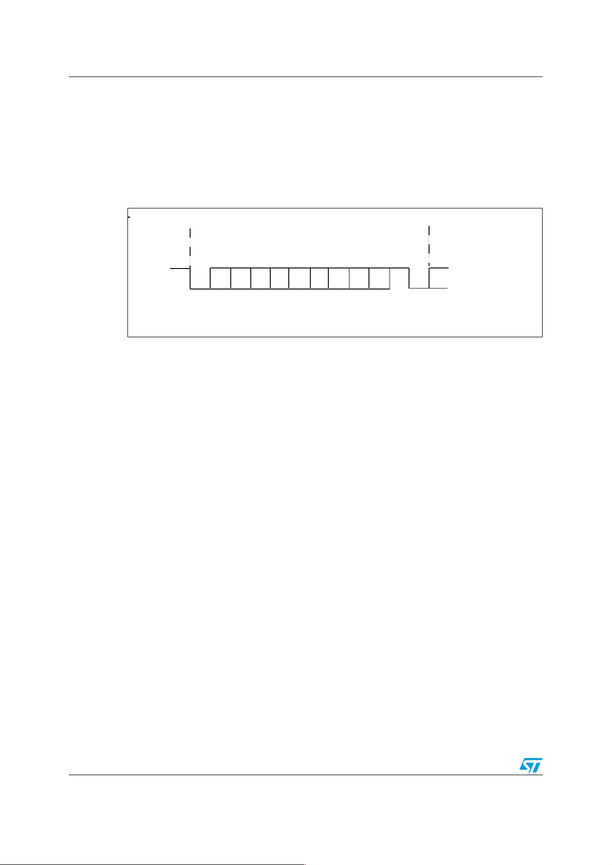
stop bit. The structure of a data frame is given in Figure 1.
Figure 1. Nine-bit data word with one stop bit
Next data frameData frame
Start
bit
Bit0 Bit8Bit7Bit6Bit5Bit4Bit3Bit2Bit1
Stop
bit
Next
start
bit
ai15043
8/33
Page 9

AN2800 Data transmission
4 Data transmission
The UART emulator can transmit data words of either eight or nine bits depending on the
8/9 control bit value. When the 8/9 bit is set, word length is nine bits. In this case the 9th bit
(the MSB) has to be specified in the data argument of the send function. If this is not done,
the MSB is sent as 0. For example, SW_UART_Send(0x1FF) sends the MSB as 1, whereas
SW_UART_Send(0xFF) sends the MSB as 0.
The transmitter is enabled during the initialization phase by setting the transmitter enable bit
(TE) of the UART_CR register. Once this is done, the data is output serially on the
UART_TX pin, each time the send function is called. The TC (transmission complete) flag
must be set before calling the send function, otherwise, the data are not transmitted.
Normally, a zero TC flag indicates that a transmission is ongoing. Therefore, it is necessary
to wait until the current transmission is finished before sending the next one.
During a transmission, the data shifts out the least significant bit (LSB) first on the UART_TX
pin, TIMER3_CC2. Every data word is preceded by a stop and a start bit which are logic
level low for a one-bit period. The data frame is terminated by a configurable number of stop
bits.
The stop bits listed in Section 4.1 below are supported by the UART emulator. A more
detailed description of the send function is provided in Section 7: The UART emulator
software algorithm on page 14.
4.1 Configurable stop bits
The number of stop bits (SB) that can be transmitted with every data frame are programmed
by the SB control bit of the control register (see Section 7.1.1: UART_CR on page 15).
● 1 stop bit: This is the default number of stop bits where the SB control bit is set to zero.
● 2 stop bits: This is supported by setting the SB control bit to one.
4.2 General procedure for sending a data word
1. Program the UART_CR 8/9 bit to define the word length
2. Program the UART_CR SB bit to define the stop bit number
3. Set the UART_CR TE bit to enable the transmitter
4. Select the desired baud rate
5. Enable all the interrupts
6. Call the init function (see Section 7.2: UART emulator initialization function on
page 17), specifying the UART_CR register and the baud rate.
7. Clear the CFLAG (consecutive flag) for a single byte transmission
8. Call the send function, specifying the data word to send
9. For consecutive data word transmissions, wait for the TC flag to be set before calling
the send function again. In this case do not clear the CFLAG between two consecutive
send calls.
9/33
Page 10

Data transmission AN2800
4.3 Single byte transmission
During a transmission the TC flag is cleared. While it is clearing, a send call does not trigger
a further transmission instead, it checks the TC flag before starting a transmission.
When no transmission is taking place the send routine clears the TC flag and starts a data
frame transmission. When a frame transmission is almost complete (at the beginning or at
the end of the MSB transmission according to the selected number of stop bits) the TC flag
is set. The TC flag is cleared automatically by a write to the UART_SR register, each time
the send function is called. The CFLAG must be cleared before a single data word
transmission as it impacts on the transmission start time reference.
4.4 Consecutive byte transmissions
By default, the transmitter is configured to send consecutive data words. Between two
consecutive send calls, a wait condition for the TC flag has to be inserted. In this case, the
CFLAG does not have to be cleared.
10/33
Page 11

AN2800 Data reception
5 Data reception
The UART emulator can receive data words of either eight or nine bits. When the 8/9 bit is
set, words are nine bits long and all data bits, including the MSB, are stored in an array
called the Receiver_Data_Register.
5.1 Receiver data register full (RDRF)
In receiver or full duplex mode, the data input pin waits for a start bit. Once a valid start bit is
detected, the middle of each data bit is read, using a majority voting system based on three
samples, to define the correspondent bit value. A falling edge, due to a glitch, is not
considered as a valid start bit and the reading procedure is aborted. During a reception,
data shifts in the LSB first through the UART_RX pin. At the end of a reception the RDRF
flag is set to indicate that the incoming data word is ready to be read. If the receiver data
register is not going to be read through the read function, the RDRF flag must be cleared
after reading the data word directly from the array. In this way it is always known when an
incoming frame is ready to be read through the RDRF flag.
5.2 General procedure for receiving a data word
1. Program the UART_CR 8/9 bit to define the word length
2. Set the UART_CR RE bit to enable the receiver
3. Select the desired baud rate
4. Enable all interrupts
5. Call the init function (see Section 7.2: UART emulator initialization function on
page 17), specifying the UART_CR register and the baud rate.
6. Once the init function has occurred, the data input pin polls for an incoming data frame.
When a data word is received, the following occurs:
● The RDRF bit is set. It indicates that the content of the receiver data register is ready to
be read.
● The FE flag can be set if a frame error occurs
● During reception of data bits, the NF flag can be set, indicating the presence of noise
on the RX line.
● The received data word can be read directly from the Receiver_Data_Register as soon
as the RDRF flag is set. Otherwise, the read function could be used for the same
purpose. This routine automatically waits for the RDRF flag to be set and returns the
received data word as an integer value. The Read() function can be used to transfer the
received data word, stored in the Receiver_Data_Register array, into an integer
variable. If this function is used in a program loop which transmits continuously, it is
necessary to clear the CFLAG before the send function and directly after the Read()
function call (see Section 9.2 on page 31). Clearing the CFLAG introduces a very small
delay between the transmission of two data frames.
11/33
Page 12

Data reception AN2800
5.3 Noise error
Over-sampling techniques are used for data recovery and to discriminate between valid
incoming data and noise.
When noise is detected on each data bit:
● The UART_SR NF bit is set
● The invalid data is still available in the Receiver_Data_Register
The UART_SR NF bit rises as soon as noise appears during the reception of each bit. In
other words, this flag is set or reset according to the values of three samples taken in the
middle of each bit. The NF flag can also be reset by software.
5.4 Frame error
A frame error is detected when the first stop bit of an incoming data frame is not recognized
at the expected time due to invalid incoming data frames or excessive noise.
When a framing error is detected:
● The UART_SR FE bit is set
● The invalid data is still available in the Receiver_Data_Register
If a framing error occurs, the UART_SR FE bit rises at the end of a data frame reception.
The bit is automatically reset by the next valid data frame or via software.
5.5 Configurable stop bits during reception
Only the first stop bit is sampled to detect a valid data frame regardless of the SB bit value.
If a framing error is detected, the FE flag is set. Otherwise, the FE flag is reset. The RDRF
flag is always set at the end of the first stop bit.
12/33
Page 13

AN2800 Baud rate generator
6 Baud rate generator
The transmitter and receiver are driven by a common baud rate generator, the timer3
counter, which ensures correct transmission and reception timings. The timer3 counter is
enabled when at least one enable bit for the transmitter or receiver is set.
Data transfer velocity is expressed in terms of baud rate. In binary coding terms, baud rate is
the number of bits per second (bps). Both the receiver (RX) and transmitter (TX) are set to
the same baud rate, which is programmed during the initialization phase according to the
formula in Equation 1.
Equation 1
One_bit_Delay = CLK_GetClockFreq()/bps
Note: The above formula is correct only if the clock frequency of timer3 is equal to f
The bps divider is an unsigned integer that is coded by the bps argument of the initialization
function. A one-bit delay represents the number of timer3 counter clock cycles within one-bit
period. Once one-bit length has been defined in terms of timer3 clock cycles, the timer
manages all the sends and receives according to one-bit length. To achieve the maximum
allowed baud rate of 28800, timer3 is clocked with a 16 MHz clock source. The above
formula yields the result given in Equation 2.
Equation 2
One_bit_Delay = 16 MHz/28800 = 02 2Bh
Six standard baud rates are supported by the UART emulator:
● 1200 bps
● 2400 bps
● 4800 bps
● 9600 bps
● 19200 bps
● 28800 bps
MASTER
.
13/33
Page 14

The UART emulator software algorithm AN2800
7 The UART emulator software algorithm
The UART emulator software algorithm allows data words to be received and/or transmitted
in an NRZ, asynchronous, serial format through properly configured timer3 capture and
compare events. In particular, capture and compares events on the CC1 and CC2 channels
of timer3, allow serial data to be simultaneously received and transmitted (full duplex mode).
The transmission or reception process, for any bit, is handled by the capture/compare
interrupt service routine (irq16) of timer 3.
The UART software only works through interrupts, thus, the main program is free to
accomplish other tasks between two consecutive interrupts. To avoid another maskable
interrupt request interfering with an ongoing transmission or reception, the timer3
capture/compare interrupt vector should be configured with the highest software priority.
Before sending or receiving a data word, the UART emulator must be properly configured
using the initialization function.
The UART emulator is controlled through three software registers:
● UART control register (UART_CR)
● UART status register (UART_SR)
● UART data register (Receiver_Data_Register)
14/33
Page 15

AN2800 The UART emulator software algorithm
7.1 UART emulator software registers
7.1.1 UART_CR
The UART_CR allows the number of stop bits, the operating mode, and the data word length
to be selected through the stop bit, the receiver enable/transmitter enable bit, and bit 8/9
respectively (see Ta bl e 1 ). In the example below, the UART_CR configures the UART
emulator in full duplex mode with a data word length of nine bits and two stop bits
UART_CR example
Bit 7Bit 6Bit 5Bit 4Bit 3Bit 2Bit 1Bit 0
-SB- - -RETE8/9
01000111
Table 1. UART_CR description
Bit Bit name Function
7--
Stop bit
6SB
Sets the stop bit number
0: One stop bit
1: Two stop bits
5--
4--
3--
Receiver enable bit
2RE
Sets the operating mode to receive data
0: Receive disabled
1: Receiver enabled
Transmitter enable bit
1TE
Sets the operating mode to transmit data
0: Transmitter disabled
1: Transmitter enabled
Bit 8/9
08/9
Sets the data word length
0: 8 data bits
1: 9 data bits
15/33
Page 16

The UART emulator software algorithm AN2800
7.1.2 UART_SR
The UART_SR indicates the status of a transmission and/or a reception through the
following four flags: TC, RDRF, NF, and FE.
See UART_SR example and Ta bl e 2 . The UART_SR example shows the presence of a
frame error in the last data frame received.
UART_SR example
Bit 7Bit 6Bit 5Bit 4Bit 3Bit 2Bit 1Bit 0
- - TC RDRF - - NF FE
00110001
Table 2. UART_SR description
Bit Bit name Function
7--
6--
Transmission complete flag
5TC
4RDRF
3--
Indicates the end of a transmission
0: Transmission in progress
1: Transmission complete
Receiver data register full flag
Indicates that a reception has been completed and that the result is
ready to be read
0: Reception not completed and Receiver_Data_Register not ready to
be read.
1: Reception completed and Receiver_Data_Register ready to be read.
2--
Noise error flag
1NF
Allows noise error detection
0: No error detected
1: Error detected
Frame error flag
0FE
Allows frame error detection
0: No error detected
1: Error detected
7.1.3 Receiver_Data_Register
The receiver data register is an array that stores the incoming data word.
16/33
Page 17

AN2800 The UART emulator software algorithm
7.2 UART emulator initialization function
Once the interrupts have been enabled (by a RIM instruction), the UART emulator has to be
configured before transmitting or receiving a data word. This is done by calling its init
function. This function requires two arguments:
● An 8-bit arguement, representing the UART_CR, which allows the data word length,
the number of stop bits, and the operating mode (transmitter mode, receiver mode, or
full duplex mode) to be defined.
● A second arguement, representing the data exchange velocity (the baud rate) which is
expressed in bits per second (bps).
For example, the following code configures the UART emulator in full duplex mode with an
8-bit data word length and one stop bit at a transfer rate of 19200 bps:
enableInterrupts();
SW_UART_Init(RX_ON|TX_ON,19200);
The init function calculates one-bit length in terms of timer3 counter clock cycles. The result
depends on the counter clock frequency, which in the current example code is equal to
f
MASTER
Its value is automatically fixed as described in Section 6: Baud rate generator on page 13.
The half bit length is also calculated, because it is necessary for reading the start bit of an
incoming data frame. To achieve high data transfer speeds, a 16 MHz master clock source
should be used
function is set to one. A higher f
According to the selected operating mode, channel 1 and 2 of timer3 are configured as
shown in Ta bl e 3 .
. One-bit length provides information about the transmission and reception velocity.
(a)
. For this reason the high-speed internal (HSI ) clock divider in the init
MASTER
further improves application performances.
a. If the master clock source selected to drive the microcontroller is an external resonator oscillator with a
frequency different from 16 MHz, the HSE_VALUE constant in the STM8_CLK.h file at line 214 must be
updated with the frequency of the external clock.
17/33
Page 18

The UART emulator software algorithm AN2800
Table 3. Configuring channels 1 and 2 of timer2
Operating mode Channel 1/2 Result
Output compare mode activated to put CC2 in high state
TX mode only
(TE = 1 and RE = 0)
RX mode only
(TE = 0 and RE = 1)
Full duplex mode
(TE = 1 and RE = 1)
TIMER3_CC2
TIMER3_CC1 Input capture mode disabled. RDRF flag set to 0.
TIMER3_CC2
TIMER3_CC1
TIMER3_CC2
TIMER3_CC1
(TX line idle) ready to send a data word. After
initialization the TC flag is set to 1.
Forced output compare mode activated to maintain the
TX line in idle state. After initialization the TC flag is set to
0.
Input capture mode triggered by a falling edge to detect a
start bit. The RDRF flag is set to 1 at the end of a
reception.
Output compare mode activated to put CC2 in high state
(TX line idle) ready to send a data word. After
initialization the TC flag is set to 1.
Input capture mode triggered by a falling edge to detect a
start bit. The RDRF flag is set to 1 at the end of a
reception.
The timer3 counter is enabled only if at least one operating mode is selected. Otherwise the
counter does not run. During the initialization phase, if the transmitter is enabled, one data
word (FFh or 1FFh according to the selected data word length) is sent on the TX line
(b)
.
After the init routine execution, the UART emulator is ready to operate in the selected
operating mode.
The following code configures the UART emulator in receiver mode with a 9-bit data word
length, and two stop bits at a transfer rate of 28800 bps.
enableInterrupts();
SW_UART_Init(RX_ON|TX_ON|W9|SB_2,28800);
b. Depending on the TX pin status, the preamble transmitted (FFh of 1FFh) may not be correctly disriminated by
the receiver.
18/33
Page 19
AN2800 The UART emulator software algorithm
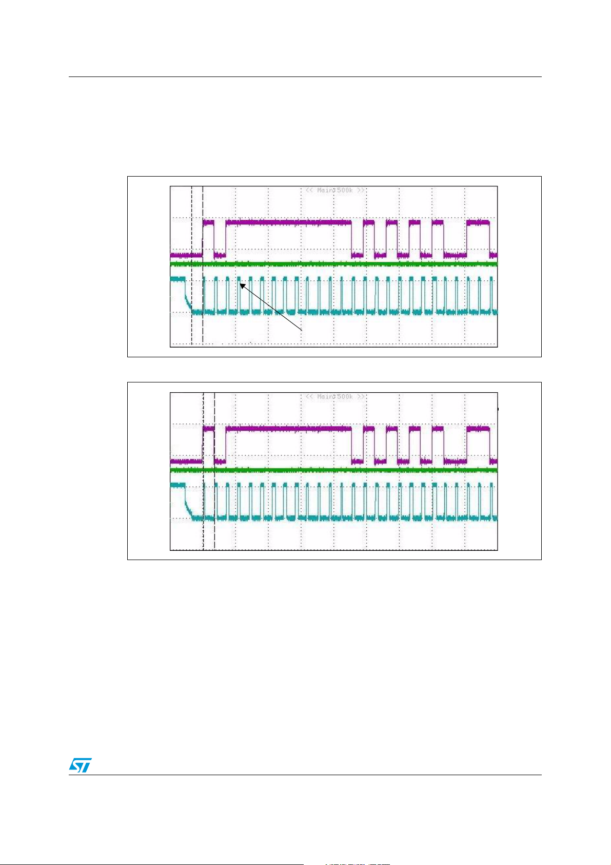
7.2.1 Transmission time line
Figure 2, Figure 3, Figure 4, and Figure 5 show the first UART transmission during the
initialization phase. In this example, the transmitter is configured to send a 9-bit data word
with two stop bits. It sends the data word 1 FFh at a baud rate of 28800 bps.
Figure 2. One bit delay
Data frame
4X 35.074 µs
Figure 3. Stop bit
Output compare two interrupts
19/33
Page 20

The UART emulator software algorithm AN2800
Figure 4. Start bit
Figure 5. Two stop bits
20/33
Page 21

AN2800 The UART emulator software algorithm
7.3 UART emulator de-initialization functions
There are two UART emulator de-initialization functions:
● deinit
● deinit1
The first function, deinit, disables the UART emulator de-initializing timer3 and resetting the
UART_CR and UART_SR.
The second function, deinit1, must be used in the software process to change the UART
operating mode. It changes the UART operating mode as follows: The deinit1 function is
called. This is followed by a call to the init function (with the new UART settings).
Note: Before resetting the UART registers and de-initializing timer3, the init function waits for the
end of the previous data word transmission and/or an ongoing reception.
The deinit1 function can be called at any time including directly right after a send call. In the
former case, the CFLAG must be cleared before calling the deinit1 function. Changing the
operating mode takes a few milliseconds (@16 MHz). This includes timer3 deinit1 and
UART init execution times.
7.3.1 Changing the operating mode: Example 1
SW_UART_Send(0xaa);
while (!(UART_SR & 0x20)) {nop();}
SW_UART_DeInit1();
SW_UART_Init(RX_ON|TX_ON,9600);
SW_UART_Send(0x55);
while (!(UART_SR & 0x20)) {nop();}
7.3.2 Changing the operating mode: Example 2
SW_UART_Send(0xaa);
while (!(UART_SR & 0x20)) {nop();}
.................
CFLAG=0x00;
SW_UART_DeInit1();
SW_UART_Init(RX_ON|TX_ON,9600);
.................
CFLAG=0x00;
SW_UART_Send(0x55);
while (!(UART_SR & 0x20)) {nop();}
21/33
Page 22

The UART emulator software algorithm AN2800
7.4 Functional description of data transmission
If the TC flag is set and a send function is called, the transmission sequence is as follows:
● Wait for a one-bit delay
● Generate a stop bit
● Generate a start bit
● Generate a data word: Eight or nine data bits starting from the LSB.
This transmission sequence insures a correct data frame structure and a correct stop and
start condition irrespective of the level of the TX line. Each bit is transmitted on the TX line
for the same duration which is fixed to a delay of one-bit. The data frame structure is shown
in Figure 6. The number of stop bits and the data word length can vary (see Section 7.1.1:
UART_CR on page 15).
Figure 6. Data frame structure
The one-bit delay followed by one stop bit at the beginning of a data frame, allows the
previous data frame to end with one or two stop bits according to the SB value.
Transmission occurs on the TIMER3_CC2 pin configured in output compare active or
inactive mode according to the bit value to be sent (either logic 1 or 0).
All data bits, including the start and stop bits, are sent on the TX line (TIMER3_CC2) for a
time period which is defined by the time span between two output compare events. This time
period is set to a one-bit delay.
22/33
Page 23

AN2800 The UART emulator software algorithm
7.4.1 Sending a data frame
To send a data frame, the send function must be called and the TC flag must be set. The TC
flag can only be set if the transmitter has been enabled during the initialization phase. It is
set at the beginning or at the end of the MSB transmission according to the SB control bit
value. The arguement of the send function represents the data word that has to be sent.
Only the first eight or nine bits of the routine arguement are transmitted according to the 8/9
control bit value. During transmission, the TC flag is cleared to indicate that transmission is
in progress.
To send another data word, the user must wait for the end of the previous transmission (for
the TC flag to be set).
To transmit consecutive data frames without delay by default, the CFLAG is automatically
set at the end of each data transmission (including the transmission during the initialization
phase). When the CFLAG is set to 1, the next send function call takes the previous output
compare value as a time reference for the next data frame transmission.
Example of consecutive data frame transmission
SW_UART_Init(RX_ON|TX_ON,19200);
SW_UART_Send(0x55);
while (!(UART_SR & 0x20)) {nop();}
SW_UART_Send(0xAA);
while (!(UART_SR & 0x20)) {nop();}
SW_UART_Send(0xAA);
while (!(UART_SR & 0x20)) {nop();}
Example of transmission instruction sequence
SW_UART_Send(0x55);
While(!(UART_SR & 0x20)) {nop();}
To transmit non consecutive
each single send function call. Each time the CFLAG is cleared, the send routine takes the
counter value as a time reference. This new time reference is taken for each data frame
transmission, producing a correct non consecutive data frame transmission.
(c)
data frames the CFLAG should be cleared (set to 0) before
c. Non consecutive transmission means that there is at least one non transmission instruction betweentwo data
frame
23/33
Page 24

The UART emulator software algorithm AN2800
Examples of non consecutive data frame transmissions
Example 1:
SW_UART_Init(RX_ON|TX_ON,19200);
.................
CFLAG=0x00;
SW_UART_Send(0x55);
while (!(UART_SR & 0x20)) {nop();}
SW_UART_Send(0xAA);
while (!(UART_SR & 0x20)) {nop();}
SW_UART_Send(0xAA);
while (!(UART_SR & 0x20)) {nop();}
Example 2:
.................
CFLAG=0x00;
SW_UART_Send(0x55);
while (!(UART_SR & 0x20)) {nop();}
.................
.................
CFLAG=0x00;
SW_UART_Send(0x55);
while (!(UART_SR & 0x20)) {nop();}
24/33
Page 25

AN2800 The UART emulator software algorithm
7.4.2 Transmitting a single data word
The CFLAG is cleared to take the counter value, instead of the previous output compare
value, as a time reference (see Section 7.4.1: Sending a data frame). Next, the send
function is called and the counter value is read. The routine then adds a one-bit delay value
to the counter value which corresponds to one-bit duration in terms of counter pulses to the
counter value. After this, the send function loads the result in the output compare register
which indicates a one-bit delay. Finally, the routine clears the CC2 interrupt flag and the TC
flag.
Note: When the TC flag is set to zero, a transmission is in progress.
Before leaving the send function, the output compare interrupts of channel 2 are enabled.
When the counter reaches the output compare value for the first time, the relative output
configured in active mode goes high and an interrupt is generated. The timer3 capture
compare interrupt service routine (ISR) handles the transmission. However, before entering
the transmission, a section of the timer3 capture compare ISR together with the CC2
interrupt flag and the TC flag are checked. The first interrupt configures the channel in
output compare inactive mode to generate the start bit on the next output compare event.
This interrupt then loads a new value in the output compare register. This new value is the
previous value plus the one-bit period value. Before leaving the ISR, the CC2 interrupt flag
is cleared.
After the one-bit delay, a new output compare event is generated. In this instance the TX line
is pulled down and a new interrupt is generated. The interrupt configures the channel in
active or inactive mode according to the first data bit to be sent (the LSB). It then loads a
new value in the output compare register (the old output compare register value plus the
one-bit delay value). The CC2 interrupt flag is cleared before leaving the ISR.
The steps above are repeated for each data bit that has to be sent. At the beginning of the
MSB transmission, the number of stop bits are checked to generate one or two stop bits.
When a frame has been transmitted, the TC flag is set to allow another frame to be sent.
Note: Resetting the TE bit during a transmission has no effect on the transmission itself nor on the
UART operating mode. To disable the transmitter it is necessary to de-initialize and then reinitialize the UART emulator without the transmitter. Avoid manually modifying the TE bit
and the TC flag.
25/33
Page 26

The UART emulator software algorithm AN2800
7.5 Functional description of data reception
The reception procedure is handled by an appropriate section of the timer3 capture
compare ISR. It occurs on TIMER3_CC1 which is configured first in input capture mode and
then in output compare frozen mode (see Figure 7). The receiver must be enabled by
setting the RE bit during the initialization phase (see Section 7.2: UART emulator
initialization function on page 17). Reception begins once the receiver has been enabled
and a falling edge has occurred on TIMER3_CC1.
Figure 7. Reception on TIMER3_CC1
As soon as a falling edge is detected, an interrupt is generated and the CC1 interrupt flag is
checked. The reception section of the ISR, which is dedicated to receiving a data word, is
then entered. This section defines the sampling RX timings by disabling the captures on
TIMER3_CC1, storing the captured value of the counter in a variable, and configuring
channel 1 in output compare frozen mode (output compare mode with outputs disabled).
A half-bit period is then added to the captured counter value and the result is loaded into the
output compare register. This generates an interrupt, which initiates the routine to read the
RX line value in the middle of the first incoming bit (which should be a start bit).
An interrupt is also generated on the first CC1 output compare event. The RX line value is
read (from the middle of the expected start bit). According to the result, the reading process
can be aborted or continued.
If a high level is read, channel 1 is configured as input capture, the captures are enabled, the
CC1 interrupt flag is cleared, the ISR is exited, and the reading is aborted.
If a low level is read, the routine continues reading by loading a new value in the output
compare register which is equal to the previous content of the output compare register plus
one full bit delay. The next output compare event occurs in the middle of the first data bit
which is where the sampling process starts. During the sampling process, the RX line level
is read three times (see Figure 8). Afterwards, the bit value is decided according to a
majority voting system as described in Ta bl e 4 .
26/33
Page 27

AN2800 The UART emulator software algorithm
Figure 8. Reading the RX line level
Table 4. Bit value majority voting system
Sampled value NF Stored bit value
000 0 0
001 1 0
010 1 0
011 1 1
100 1 0
101 1 1
110 1 1
111 0 1
The ‘decided’ bit value is stored in its corresponding data array position of the receiver data
register array. Then the function (reception section of the ISR) calculates a new output
compare value to generate another interrupt and read the next data bit. The process
continues for each data frame bit including the first stop bit. The last output compare
interrupt checks the stop bit value and sets or resets the FE flag according to it. Finally,
channel 1 is once again configured in capture mode to detect the next data frame start bit.
At the end of a reception the RDRF flag is set and the received data word is available in the
Receiver_Data_Register array.
The read function checks the RDRF bit. If it is set, it transfers the array content into an
integer variable. Before leaving the read function, the RDRF bit is cleared. However, this
function slows the UART emulator, in full duplex mode, for baud rates equal to or greater
than 19200 bps.
Note: If the RE bit is disabled during a reception, the current byte reception continues to
successfully receive data. This is because after the initialization phase, a reset of the RE bit
has no effect on the emulator operating mode.
Caution: Avoid manually modifying the RE bit. To disable the receiver, it is necessary to de-initialize
and then re-initialize the UART emulator without the receiver. If the read function is not used
to read the received data word, after reading the Receiver_Data_Register array, the RDRF
flag should be cleared manually.
Note: Transmission and reception are achieved through the channel2 and channel1 interrupts of
timer3. To ensure a correct transmission and/or reception, the interrupt software priorities
should be configured to give the highest priority to the timer3 capture compare interrupt
vector.
27/33
Page 28

Connecting the UART emulator to a PC AN2800
8 Connecting the UART emulator to a PC
The UART emulator cannot be connected directly to a PC because a PC uses the RS232
standard and the UART emulator does not.
The electrical and communication protocol features of the RS232 standard are different from
those provided by the CC1 and CC2 channels of the UART emulator timers. The RS232
standard works with ±13 V whereas the UART emulator timers work with CMOS levels. Bit
polarities are also opposite. A ‘1’ bit coming from the UART emulator timers corresponds to
5 V whereas a ‘1’ bit coming from the PC corresponds to -13 V. This is true for all bits.
To overcome these problems, the ST232 is used as an interface between the PC and the
STM8A. An overview of the system is presented in Figure 9.
Figure 9. PC-ST232- STM8A system overview
1. All devices must have the same ground reference.
2. The receive data pin of the UART emulator corresponds to the TIMER3_CC1 pin whereas the transmit
data pin corresponds to the TIMER3_CC2 pin.
28/33
Page 29

AN2800 Main.c examples
9 Main.c examples
Two examples are given below of program loops from the main.c file.
Note: The code folder contains a file called Main.EXAMPLE.c which provides examples of how to
switch between different emulator configurations, how to send single and consecutive data
frames, and how to poll for an incoming data frame.
9.1 Example 1
The following code is an example of data transmissions at different operating modes.
/* Includes -------------------------------------------------------
-----------*/
#include "stm8_lib.h"
#include "stm8_sw_uart.h"
/* Private variables-----------------------------------------------
----------*/
u16 RX_data;
extern u8 CFLAG;
/* Public functions -----------------------------------------------
----------*/
void main(void)
{
u8 ji;
/* Enables all the interrupts ---------------------------------
-------------*/
enableInterrupts();
/* Initializes the sw_uart specifying the USART_CR value and
the baud rate value, arguments of the SW_UART_Init function:
SW_UART_Init(UART_CR value,BAUD_RATE value) ---------------*/
SW_UART_Init(RX_ON|TX_ON|SB_2,19200);
/* Sends three data frames------------------------------------
------------ */
SW_UART_Send(0x55);
while (!(UART_SR & TC_FLAG)) {nop();}
/* The following for loop represents an instruction between two
send calls--------------*/
for (ji=0;ji<255;ji++) nop();
29/33
Page 30

Main.c examples AN2800
/* If between two send calls there is at least one instruction,
remember to clear the CFLAG-----------------------------------
-------------------------*/
CFLAG=0x00;
SW_UART_Send(0xaa);
while (!(UART_SR & TC_FLAG)) {nop();}
SW_UART_Send(0x00);
while (!(UART_SR & TC_FLAG)) {nop();}
/* Changes the emulator operating mode------------------------
---------- */
SW_UART_DeInit1();
SW_UART_Init(RX_ON|TX_ON|W9,28800);
/* Sends one data frame---------------------------------------
-------------- */
SW_UART_Send(0xBB);
while (!(UART_SR & TC_FLAG)) {nop();}
/* Changes the emulator operating mode------------------------
-------- */
SW_UART_DeInit1();
SW_UART_Init(RX_ON|TX_ON|W9,9600);
/* Sends two data frames--------------------------------------
------------ */
SW_UART_Send(0x1ff);
while (!(UART_SR & TC_FLAG)) {nop();}
SW_UART_Send(0x00);
while (!(UART_SR & TC_FLAG)) {nop();}
while (1)
{
/* Reads incoming data frames---------------------------------
---------- */
RX_data=SW_UART_Read();
}
}
30/33
Page 31

AN2800 Main.c examples
9.2 Example 2
The following code is an example of a continuous data transmission and polling of an
incoming data frame.
while (1)
{
/* Remember to clear CFLAG when continues transmission are
interrupted by one or more instructions--------------------
-----*/
CFLAG=0x00;
SW_UART_Send(0x55);
while (!(UART_SR & 0x20)) {nop();}
SW_UART_Send(0x55);
while (!(UART_SR & 0x20)) {nop();}
SW_UART_Send(0xaa);
while (!(UART_SR & 0x20)) {nop();}
/* Reads incoming data frames, if RDRF flag is set to one--
--*/
RX_data=SW_UART_Read();
}
31/33
Page 32

Revision history AN2800
10 Revision history
Table 5. Document revision history
Date Revision Changes
04-Nov-2008 1 Initial release
32/33
Page 33

AN2800
Please Read Carefully:
Information in this document is provided solely in connection with ST products. STMicroelectronics NV and its subsidiaries (“ST”) reserve the
right to make changes, corrections, modifications or improvements, to this document, and the products and services described herein at any
time, without notice.
All ST products are sold pursuant to ST’s terms and conditions of sale.
Purchasers are solely responsible for the choice, selection and use of the ST products and services described herein, and ST assumes no
liability whatsoever relating to the choice, selection or use of the ST products and services described herein.
No license, express or implied, by estoppel or otherwise, to any intellectual property rights is granted under this document. If any part of this
document refers to any third party products or services it shall not be deemed a license grant by ST for the use of such third party products
or services, or any intellectual property contained therein or considered as a warranty covering the use in any manner whatsoever of such
third party products or services or any intellectual property contained therein.
UNLESS OTHERWISE SET FORTH IN ST’S TERMS AND CONDITIONS OF SALE ST DISCLAIMS ANY EXPRESS OR IMPLIED
WARRANTY WITH RESPECT TO THE USE AND/OR SALE OF ST PRODUCTS INCLUDING WITHOUT LIMITATION IMPLIED
WARRANTIES OF MERCHANTABILITY, FITNESS FOR A PARTICULAR PURPOSE (AND THEIR EQUIVALENTS UNDER THE LAWS
OF ANY JURISDICTION), OR INFRINGEMENT OF ANY PATENT, COPYRIGHT OR OTHER INTELLECTUAL PROPERTY RIGHT.
UNLESS EXPRESSLY APPROVED IN WRITING BY AN AUTHORIZED ST REPRESENTATIVE, ST PRODUCTS ARE NOT
RECOMMENDED, AUTHORIZED OR WARRANTED FOR USE IN MILITARY, AIR CRAFT, SPACE, LIFE SAVING, OR LIFE SUSTAINING
APPLICATIONS, NOR IN PRODUCTS OR SYSTEMS WHERE FAILURE OR MALFUNCTION MAY RESULT IN PERSONAL INJURY,
DEATH, OR SEVERE PROPERTY OR ENVIRONMENTAL DAMAGE. ST PRODUCTS WHICH ARE NOT SPECIFIED AS "AUTOMOTIVE
GRADE" MAY ONLY BE USED IN AUTOMOTIVE APPLICATIONS AT USER’S OWN RISK.
Resale of ST products with provisions different from the statements and/or technical features set forth in this document shall immediately void
any warranty granted by ST for the ST product or service described herein and shall not create or extend in any manner whatsoever, any
liability of ST.
ST and the ST logo are trademarks or registered trademarks of ST in various countries.
Information in this document supersedes and replaces all information previously supplied.
The ST logo is a registered trademark of STMicroelectronics. All other names are the property of their respective owners.
© 2008 STMicroelectronics - All rights reserved
STMicroelectronics group of companies
Australia - Belgium - Brazil - Canada - China - Czech Republic - Finland - France - Germany - Hong Kong - India - Israel - Italy - Japan -
Malaysia - Malta - Morocco - Singapore - Spain - Sweden - Switzerland - United Kingdom - United States of America
www.st.com
33/33
 Loading...