

Page 1

AN2797
Application note
PCB layout guidelines for SPEAr600
Introduction
SPEAr600 is a 23 x 23 mm PBGA420 device with 1 mm ball pitch. It is a member of the
®
SPEAr
at up to 333 MHz, an external DDR2 memory interface and a full set of powerful on-chip
peripherals.
This application note provides guidelines for successfully designing the PCB layout for
SPEAr600. It covers following main topics:
■ Power integrity
■ DDR memory interface
■ USB signals
■ GPIO/CLD signals
■ External clock
family of 32-bit embedded MPUs. The device features dual ARM926 cores running
Placement guidelines for the decoupling capacitors are provided in Appendix A.
December 2009 Doc ID 14841 Rev 1 1/23
www.st.com
Page 2

Contents AN2797
Contents
1 Power integrity . . . . . . . . . . . . . . . . . . . . . . . . . . . . . . . . . . . . . . . . . . . . . . 4
1.1 PCB stack up . . . . . . . . . . . . . . . . . . . . . . . . . . . . . . . . . . . . . . . . . . . . . . . 4
1.2 Via padstack . . . . . . . . . . . . . . . . . . . . . . . . . . . . . . . . . . . . . . . . . . . . . . . . 4
1.3 Part orientation and placement . . . . . . . . . . . . . . . . . . . . . . . . . . . . . . . . . 4
1.4 Ground and power supply connections . . . . . . . . . . . . . . . . . . . . . . . . . . . 5
2 DDR memory interface . . . . . . . . . . . . . . . . . . . . . . . . . . . . . . . . . . . . . . . 6
2.1 DRAM power decoupling . . . . . . . . . . . . . . . . . . . . . . . . . . . . . . . . . . . . . . 6
2.2 Data signal routing . . . . . . . . . . . . . . . . . . . . . . . . . . . . . . . . . . . . . . . . . . . 7
2.3 Trace length matching . . . . . . . . . . . . . . . . . . . . . . . . . . . . . . . . . . . . . . . . 8
2.4 Trace length matching, dual DRAM configuration . . . . . . . . . . . . . . . . . . 10
2.5 Return path integrity . . . . . . . . . . . . . . . . . . . . . . . . . . . . . . . . . . . . . . . . . 11
2.6 Clock routing . . . . . . . . . . . . . . . . . . . . . . . . . . . . . . . . . . . . . . . . . . . . . . 12
2.7 Vref routing . . . . . . . . . . . . . . . . . . . . . . . . . . . . . . . . . . . . . . . . . . . . . . . . 12
2.8 Observability . . . . . . . . . . . . . . . . . . . . . . . . . . . . . . . . . . . . . . . . . . . . . . 13
3 USB interface . . . . . . . . . . . . . . . . . . . . . . . . . . . . . . . . . . . . . . . . . . . . . . 14
3.1 USB routing . . . . . . . . . . . . . . . . . . . . . . . . . . . . . . . . . . . . . . . . . . . . . . . 14
3.2 USB decoupling and reference resistor . . . . . . . . . . . . . . . . . . . . . . . . . . 15
3.3 USB Device Vbus . . . . . . . . . . . . . . . . . . . . . . . . . . . . . . . . . . . . . . . . . . . 16
4 GPIO and CLD interface considerations . . . . . . . . . . . . . . . . . . . . . . . . 17
5 Using an external clock . . . . . . . . . . . . . . . . . . . . . . . . . . . . . . . . . . . . . 18
5.0.1 External clock signal requirements . . . . . . . . . . . . . . . . . . . . . . . . . . . . 18
5.0.2 Voltage translation of external clock . . . . . . . . . . . . . . . . . . . . . . . . . . . 18
5.0.3 TDR test traces . . . . . . . . . . . . . . . . . . . . . . . . . . . . . . . . . . . . . . . . . . . 19
5.0.4 Layer order check . . . . . . . . . . . . . . . . . . . . . . . . . . . . . . . . . . . . . . . . . 19
Appendix A Low-inductance decoupling capacitor layout . . . . . . . . . . . . . . . . . 20
A.1 0402 compact land pattern . . . . . . . . . . . . . . . . . . . . . . . . . . . . . . . . . . . . 20
A.2 Low inductance layout for decoupling capacitors . . . . . . . . . . . . . . . . . . . 21
2/23 Doc ID 14841 Rev 1
Page 3

AN2797 Contents
Revision history . . . . . . . . . . . . . . . . . . . . . . . . . . . . . . . . . . . . . . . . . . . . . . . . . . . . 22
Doc ID 14841 Rev 1 3/23
Page 4

Power integrity AN2797
1 Power integrity
One of the most important requirements of a reliable high-speed memory interface, and
most commonly underestimated, is a low impedance, wide bandwidth power supply at the
power and ground balls of the devices. Achieving the necessary performance requires the
minimizing of all parasitic inductances found in power delivery and grounding connections,
exploiting various techniques to provide low impedance paths, and attention to controlling
plane resonances.
A solid unbroken ground plane located close to the high-speed devices in the PCB layer
stack is critical. The ground plane must not have large gaps anywhere in the area of the
interface. Be especially aware of overlapping anti-pads that can create an extended gap in
the internal plane layers.
A power plane closely spaced to the ground plane greatly aids the high-frequency
decoupling by providing a low inductance path between a capacitor and the device's power
balls.
All high-frequency decoupling capacitors should utilize a low-inductance layout.
1.1 PCB stack up
Stack up should include a closely spaced power/ground plane pair. A minimum of 6 layers is
necessary.
Recommendation:
Layer 1: signal
Layer 2: ground plane, unbroken
Layer 3: power plane/islands, signals
Layer 4: signal/power routing
Layer 5: ground plane, unbroken
Layer 6: signal
Dielectric thickness should be selected to support required signal trace characteristic
impedances and power plane capacitance/inductance. Resonance analysis should be
performed on all plane cavities.
1.2 Via padstack
Via padstack dimensions should support density requirements. Anti-pad diameter should be
small enough to allow an adequate copper web between clearance holes of adjacent vias,
and still meet PCB fabrication tolerances.
1.3 Part orientation and placement
The DRAM placement and orientation should be given priority over other unassociated
components in order to minimize trace lengths. Closely following the signal trace routing
guidelines allows trace lengths to be reduced.
4/23 Doc ID 14841 Rev 1
Page 5

AN2797 Power integrity
1.4 Ground and power supply connections
For proper operation of devices, it is critical provide a very low impedance wide bandwidth
connection to ground and the voltage supplies. To achieve this it is necessary to minimize
inductance between the device power and ground balls and the PCB ground plane and
decoupling network.
The above guideline also applies to other critical components: termination resistors,
decoupling capacitors, ICs, multiple ground or power pins from the same IC.
Each ground ball should be directly connected to the PCB ground plane with its own via. Do
not share vias between multiple ground balls. An exception to this rule is the center 6x6
ground ball grid, which should have a fully populated ground via grid between the balls and
the surface layers can be filled.
Each power ball should be directly connected to the PCB decoupling network with its own
via. Do not share vias between multiple power balls except when multiple power balls are
adjacent to each other and are connected to the same voltage plane. In any case, use the
maximum number of vias that space allows.
To avoid cross-contamination of ground or power supplies between different devices (for
example, an IC and a termination resistor), multiple ground or power balls should not share
ground connections. Each ball/pin should have their own via to the ground or power plane,
not a shared via. Power and ground connections should not simply be connected to surface
layer copper fill areas - these are not good low impedance paths at high-frequencies.
Ball to via trace: Each ground and power ball should be connected to it's via with a short,
wide trace. It is critical to minimize trace length and maximize trace width. Trace length
should be less than 1 mm in the ball field, 0.25 mm outside a ball field, Trace width should
be wide. Do not simply connect ground or power balls to surface fill areas. A close, direct via
to the ground or power plane is necessary. In cases where it is not possible to achieve this
length, there is a relatively high impedance. Every effort should be made to minimize the
length, and to consider only power connections requiring lower bandwidth for high
impedance power connections.
Ferrite beads and RC filters: The perceived need for ferrite beads and RC filters is very
often the result of poor grounding and power supply decoupling, resulting in excess noise on
power rails. A well-designed power delivery network eliminates the need for these remedies.
Doc ID 14841 Rev 1 5/23
Page 6

DDR memory interface AN2797
2 DDR memory interface
2.1 DRAM power decoupling
A low impedance wide bandwidth power delivery network (PDN) is critical for the proper
operation of high-speed ICs such as SPEAr and DDR memory. If the PDN impedance is too
high or does not have sufficient bandwidth, this affects the logic performance, resulting in
ground and rail bounce, slower rise/fall times of both I/O and internal logic, which in turn
result in delayed timing of events. These timing delays, from inadequate ground and power,
subtract directly from the specified timing budget, which in turn can result in failure of the
interface.
To achieve a low impedance, wide bandwidth power delivery network, it is critical to use
appropriate decoupling capacitors and capacitor layout. A large portion of the power
delivery network's frequency spectrum is above the series resonant frequency of the
decoupling capacitors, where they are inductive. The PCB layout for decoupling capacitors
is also inductive, and is a larger inductance than the capacitor itself. It is necessary to select
capacitors with low inherent inductance (small package size), a lossy dielectric, and a PCB
layout that provides the lowest possible inductance. For IC core voltage and high-speed I/O
supplies (like DDR), as many capacitors should be used as can fit in the space available.
This adds many parallel paths, reducing the overall inductance seen by the IC. A small
capacitor package size and a small layout can be used to enable this.
Capacitors: Use 0402 package size to minimize the mounting inductance. The small 0402
package frees more board space, which is essential in high-density areas for more
decoupling capacitors and signal routing. A capacitance value of 100 nF or larger is
recommended, with X7R or X5R dielectric. Do not use Y5V dielectric for decoupling of midfrequency applications. A few capacitors of smaller capacitance value probably may be
necessary to suppress plane resonance. The correct value(s) to use for controlling
resonance is very dependent on the board layout and stack up and must be determined
individually for each unique PC board.
Decoupling capacitor layout: The layout of decoupling capacitors is extremely important
to minimize the induction loop formed between the capacitor and the IC power and ground
balls. The vias should be placed on the side of the capacitor lands, not the ends. The vias
should be located at minimum keepout distance and connected to the capacitor lands with a
wide trace - at least as wide as the via pad. Vias of opposite polarity should be placed as
close together as possible (minimum keepout distance) and vias of the same polarity should
be kept separated as much as possible. Following these layout guidelines can reduce the
capacitor mounting induction loop by 50% or more over a layout with vias at the end of the
capacitor lands. This is a very significant improvement, and is free. If space allows, a second
pair of vias on the opposite side of the capacitor may be added to reduce the inductance
further.
6/23 Doc ID 14841 Rev 1
Page 7
AN2797 DDR memory interface
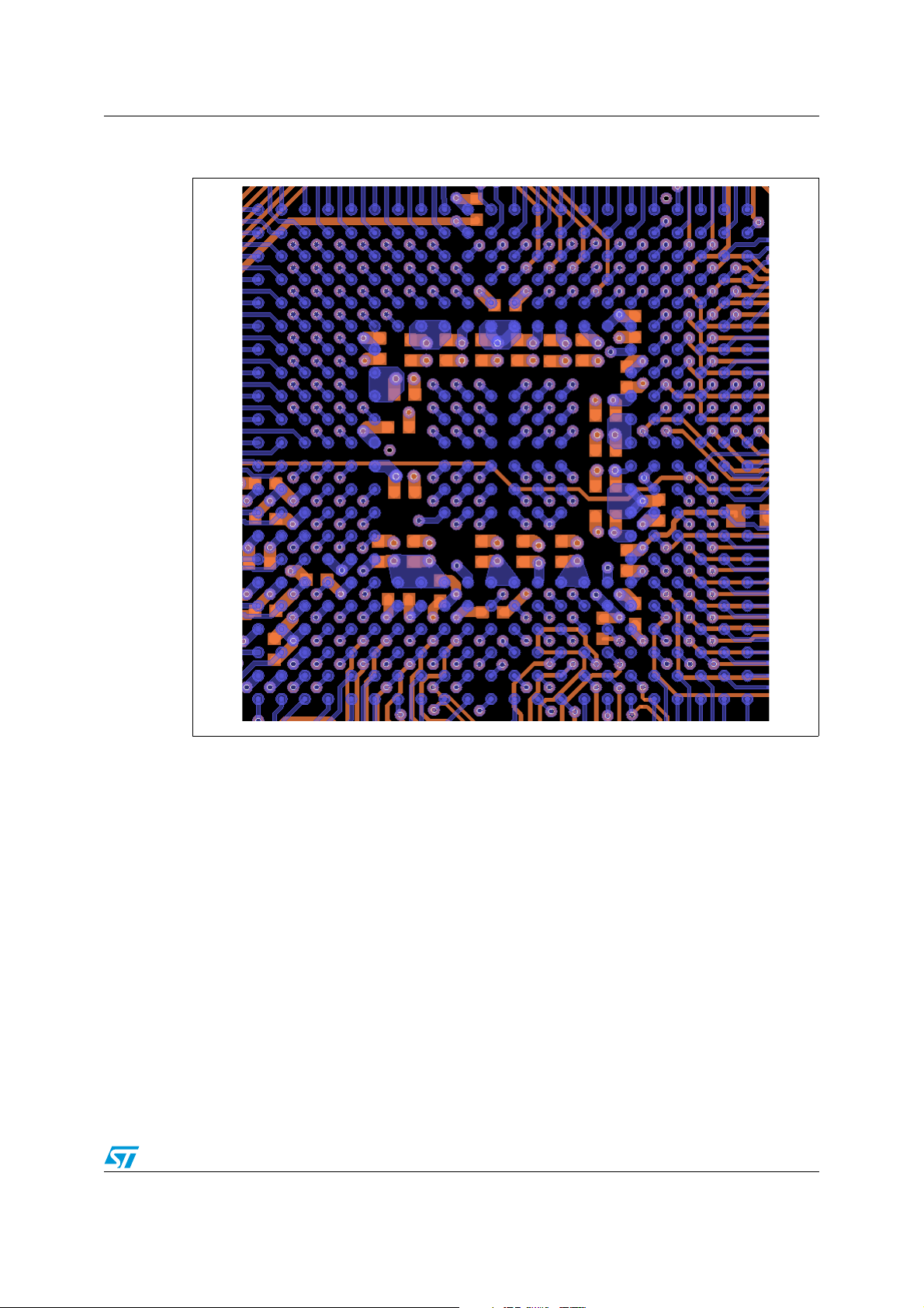
Figure 1. An example of an effective low-inductance decoupling capacitor location
and mounting layout.
2.2 Data signal routing
Signal trace geometries:
Width: 4 mil to 5mil, 0.1 mm to 0.13 mm
Minimum space: 4 mil to 5 mil, 0.1 mm to 0.13 mm
Trace to trace spacing should be increased where routing density allows to reduce crosstalk.
A minimum separation of 10 mils is recommended, except for BGA escape areas.
All signals should be routed referenced to a ground plane, not a power plane.
Do not route any DDR2 signals on top of split planes or voids of copper.
Do not route any other signals inside or on top of the area reserved for DDR.
Maintain adequate separation between DDR signals and any other signals.
Traces routed near the edge of a reference plane should maintain at least 30 mil gap to the
edge of the reference plane.
To minimize the reflection all the traces should have an impedance of 55 Ohm ± 10%.
Doc ID 14841 Rev 1 7/23
Page 8

DDR memory interface AN2797
Data lanes:
DL0: Data Lane 0 includes DQ0-DQ7, LDQS-LDQSn, LDM.
Route these signals on the same layer(s), with similarly located layer transitions if they
exist.
Length/timing skew: This set of signals traces must have their lengths matched to
within 2.5 mm or 100 mils (approximately 15 ps).
DL1: Data Lane 1 includes DQ8-DQ15, UDQS-UDQSn, UDM.
Route these signals on the same layer(s), with similarly located layer transitions if they
exist.
Length/timing skew: This set of signals traces must have their lengths matched to
within 1.5 mm or 60 mils (approximately 10 ps).
Note: Trace lengths for different clock domains are not required to be matched. Trace lengths for
DB0 do not need to match the trace lengths for DB1. Trace lengths for address/command
signals do not need to match trace lengths for DB0 or DB1. Use minimum trace lengths
within each clock domain.
CLK/CLK# and DQS/DQS#
CLK/CLK# and DQS/DQS# signals should be routed as differential pairs, length matched.
GATE_OPEN(0,1)
GATE_OPEN(0,1) must be left unconnected. Do not connect any trace, via, or test point to
balls Y13 and Y17.
2.3 Trace length matching
The SPEAr600 package substrate does not have equal-length DDR signal traces. To insure
timing alignment for all signals, both the substrate trace length plus the PCB trace length for
each signal must be equalized to meet the trace length skew tolerance for all signals within
the clock domain. A procedure for accomplishing this is provided below, along with a
worksheet to facilitate this process during DRAM interface layout. The procedure may
require an iteration if the initial longest trace must be lengthened to accommodate
serpentine routing of other signals.
To determine trace length matching requirements for each signal, follow these steps,
utilizing the worksheet provided. Ltol (maximum length difference within a clock domain) is
2.5 mm, or 100 mils.
1. Route signals per above guidelines, using the shortest possible length on all signals at
this step (length equalizing is done later).
2. Tabulate the lengths of all traces that were routed in step 1, by filling in worksheet in the
column labeled "INITIAL SHORTEST PCB TRACE LENGTH", and "PCB VIA
LENGTHS".
Note: All signals within a clock domain should have an equal number of vias and equal via lengths,
if so, then step 2 can be omitted.
3. For each clock domain, identify the trace with the maximum total length: max(trace
length + delta_length + via length). Label this trace Lmax, it is the reference length that
8/23 Doc ID 14841 Rev 1
Page 9

AN2797 DDR memory interface
other trace lengths must be adjusted to meet within Ltol. The worksheet computes
Lmax for you.
4. With the longest total trace known (Lmax), the shortest total trace length permitted
(Lmin) can be calculated by Lmin = Lmax-Ltol. Record the value of Lmin.
Note: Lmin is the total of PCB + substrate trace lengths. The worksheet computes Lmin for you.
5. Identify all signals within each data lane whose total length is less than Lmin. Tabulate
this difference. The worksheet does this for you.
6. Add the length computed in step 5 to the traces. The worksheet does this for you.
Table 1. Package substrate trace length
Package substrate trace length
Signal name Ball
(mm) (mils)
DDR_ADD_0 AB3 9.0 354
DDR_ADD_1 AB4 8.2 323
DDR_ADD_2 AA4 7.5 295
DDR_ADD_3 Y4 7.3 287
DDR_ADD_4 W4 5.7 224
DDR_ADD_5 W5 5.7 224
DDR_ADD_6 Y5 6.4 252
DDR_ADD_7 AA5 5.9 232
DDR_ADD_8 AB5 7.6 299
DDR_ADD_9 AB6 8.3 327
DDR_ADD_10 AA6 5.6 220
DDR_ADD_11 Y6 5.9 232
DDR_ADD_12 W6 5.4 213
DDR_ADD_13 W7 4.6 181
DDR_ADD_14 Y7 5.4 213
DDR_BA_0 Y9 3.9 154
DDR_BA_1 W9 4.4 173
DDR_BA_2 W10 6.6 260
DDR_RAS AB7 7.0 276
DDR_CAS AA7 6.6 260
DDR_WE AA8 5.7 224
DDR_CLKEN AB8 7.0 276
DDR_CLK_P AA9 5.4 213
DDR_CLK_N AB9 5.8 228
DDR_CS_0 Y8 5.3 209
DDR_CS_1 W8 4.8 189
Doc ID 14841 Rev 1 9/23
Page 10

DDR memory interface AN2797
Table 1. Package substrate trace length (continued)
Package substrate trace length
Signal name Ball
(mm) (mils)
DDR_ODT_0 AB2 9.7 382
DDR_ODT_1 AB1 9.9 390
DDR_DATA_0 AB11 8.2 323
DDR_DATA_1 AA10 6.0 236
DDR_DATA_2 AB10 5.6 220
DDR_DATA_3 Y10 5.3 209
DDR_DATA_4 Y11 4.9 193
DDR_DATA_5 Y12 3.5 138
DDR_DATA_6 AB12 7.0 276
DDR_DATA_7 AA12 4.9 193
DDR_DQS_0 AB13 7.6 299
DDR_nDQS_0 AA13 6.6 260
DDR_DM_0 AA11 5.2 205
DDR_GATE_0 Y13 4.0 157
DDR_DATA_8 AB15 5.7 224
DDR_DATA_9 AA16 5.3 209
DDR_DATA_10 AB16 7.8 307
DDR_DATA_11 Y16 6.4 252
DDR_DATA_12 Y15 5.5 217
DDR_DATA_13 Y14 4.8 189
DDR_DATA_14 AB14 7.1 280
DDR_DATA_15 AA14 5.8 228
DDR_DQS_1 AB17 8.8 346
DDR_nDQS_1 AA17 7.6 299
DDR_DM_1 AA15 5.7 224
DDR_GATE_1 Y17 8.3 327
2.4 Trace length matching, dual DRAM configuration
Layout of dual DRAM configurations produces additional constraints on the layout to
maintain adequate signal integrity and timing margin for a reliable interface. A "T" routing
topology should be used, keeping the branch routes to the two DRAMs as short as possible.
Length matching of traces to each device should be performed as described in Section 2.3:
10/23 Doc ID 14841 Rev 1
Page 11

AN2797 DDR memory interface
Trace length matching. Additionally, matching the length of the branch traces to each DRAM
is necessary. Mismatches in the branch length rapidly degrade signal integrity. The branch
lengths, and therefore the spacing between two memory devices, should be minimized.
Figure 2 (A, B, C) below and Tab l e 2 describe the length matching guidelines for a dual
DRAM topology.
Note: This is a guideline only, simulations should be performed using IBIS models on the actual
PCB layout to assess signal integrity and timing margin.
Figure 2. Dual DRAM "T" routing topology
Figure 2 (A) shows the topology of the data signals, Figure 2 (B) shows the topology of the
address/command/control signals with optional shunt terminations, the Figure 2 (C) shows
the topology of the differential signal CLK and DQS. Ta bl e 2 lists guidelines for length
matching of the various segments.
Table 2. Trace length matching guidelines, dual DRAM configuration
Symbol Description Max Units
tmm L1 +L2, L1+L3 length matching for all signals 15 ps
Tmm2,3 |L2-L3| length matching tolerance of branches 30 ps
2.5 Return path integrity
A continuous path for return current must exist for all DRAM signals. If not, signal delays,
significant crosstalk, and timing violations may likely result.
Doc ID 14841 Rev 1 11/23
Page 12

DDR memory interface AN2797
Signal layer changes: The preferred location for layer change vias are near the signal ball
under the device, either DRAM or SPEAr, enabling a signal return path through the device
ground vias and decoupling capacitors.
If layer changes through a via to a different reference plane are necessary away from the
devices, the layer transitions should have a nearby path for return current. If both layers are
ground, a ground via should be placed less than 1 mm from the signal via. Sharing return
current vias should be avoided. Each signal via should have its own nearby return via
(ground via). If multiple signals change layers in close proximity, each signal via should have
its own return current via. So, signal vias (and their return current vias) should be separated
from other signal vias with a stagger pattern. If routing density prevents a stagger pattern,
add as many ground vias as possible among the signal vias.
2.6 Clock routing
The clock differential signals should be routed with a pair of matched length symmetrical
traces with 110 Ohm differential impedance. The preferred clock routing layer is the top layer
with no layer transitions. The termination layout should be symmetrical, without stubs, and
located as close as possible to the clock balls on the DRAM. Three termination topologies
are shown in Figure 3. Termination resistors and decoupling capacitors should be placed in
a tight orientation to minimize trace lengths. Termination components should not share vias.
The decoupling capacitor should have a via to ground placed against the side of its ground
land. Figure 3 shows three clock termination topology options. The middle topology provides
the best tradeoff between part count and common mode rejection.
Figure 3. Clock termination topology options
2.7 Vref routing
An accurate and quiet Vref should be provided to both the DRAM and the controller. A noisy
Vref effectively introduces jitter because of this it can be a significant source of jitter-caused
timing errors. Vref is generated by a precision voltage divider. Recommended: use 0.1%
tolerance resistors. A decoupling capacitor should be placed very close (within 1 mm) to the
Vref balls. Use good capacitor layout technique. The voltage divider resistors should be
placed close to the DRAM device to minimize trace length, but not so they interfere with
other critical signal or power routing. The Vref trace should not be routed near noisy traces
12/23 Doc ID 14841 Rev 1
Page 13

AN2797 DDR memory interface
or planes. Do not place a decoupling capacitor at the junction of the resistors - only at the
Vref balls. If the Vref trace length must be long, the divider resistor value should be close to
2x the characteristic impedance of the Vref trace; 150 ohms should work well without
consuming too much power. If a long trace and/or noise coupling results between the DRAM
and controller, then it is preferable to generate a separate Vref for the DRAM and controller.
2.8 Observability
It is important to be able to observe important signals for system validation, timing, signal
quality, and debugging. Place test points on any signals or set of signals that may be needed
for these purposes. Always provide a ground via nearby any test points (<4mm) for the
probe ground. Only very small test point pads can be used, preferably just a signal via. Or if
there is insufficient space, simply a window in the solder mask over a trace can serve the
purpose. Do not create test point structures that may significantly degrade signal quality, for
example, large test points, stubs, etc.
Test points should be located at both ends of the trace (two test points per signal), as close
to the device balls as practical (a via next to the ball is preferable, untented on the bottom). It
is especially important to be able to observe signals at both the driving and receiving ends
of a trace in high-speed interfaces to validate timing parameters, and quantify driver
behavior and reflections. Observing a signal at only one end may hide important features
that are evident at the other end, even with very short traces as is the case in a point-topoint DDR interface.
In a DDR memory interface the routing and component density is too high to add test points
on all signals. A subset of DDR signals with test points is a good compromise. Test points for
the following DDR signals should be included in all designs:
● CLK/nCLK
● DQS/nDQS (all data lanes)
● DQ (Select a small number of signals that are representative of best and worst signal
paths, at least two DQ signals.)
● Address and Command (Select subset of signals that are of interest and that are
representative of best and worst signal paths.)
Doc ID 14841 Rev 1 13/23
Page 14

USB interface AN2797
3 USB interface
3.1 USB routing
USB signal trace routing should follow good high speed PCB rules and meet the
specifications for differential impedance and maximum trace delay between connector and
the SPEAr600 device.
● USB data traces should be routed with the shortest most direct path possible to their
connectors.
● USB data traces should have no resistors or magnetic components.
● USB data traces should be routed only over ground planes.
● USB data traces should never cross gaps or breaks in the return plane.
● USB data traces should never be routed under other devices or between the pins of
other devices.
● USB data vias should be widely separated from other signal vias.
● If USB data traces transition layers to a different return plane, then ground vias for the
return current should be placed very close to the signal vias.
Table 3. USB signal routing constraints
Symbol Description Min Typ Max Units
ZODiff Differential impedance
t
d_Dev
t
d_Host
t
d_match
Trace delay of device port
Trace delay of host port
Trace length mismatch 0.15/3.8 inch/mm
(1)
(1)
(1)
81 90 99 Ω
1.0 ns
3.0 ns
Number or length of stubs 0
Number of via transitions 1
Space to adjacent signal traces
Space to adjacent area fill
(4)
(2)
3h
3h
Space to edge of return plane 20 h
1. Trace delay between SPEAr and USB connector (Universal Serial Bus Specification, Revision 2.0)
2. This includes other USB data trace pairs.
3. The unit 'h' is the thickness of the dielectric separating the trace from the nearest plane.
4. Do not use "guard" traces or ground flood/fill adjacent to high speed signal traces.
(3)
(3)
(3)
Figure 4. Cross section of PCB showing minimum spacing dimensions for USB
signal traces
14/23 Doc ID 14841 Rev 1
Page 15

AN2797 USB interface
3.2 USB decoupling and reference resistor
Decoupling capacitors should be placed as close as possible to the power balls, preferably
directly under the power balls using short wide connecting traces. Placing decoupling
capacitors at a distance degrades the performance, which can result in interoperability
problems and compliance violations with the specifications.
Table 4. USB power, ground, and reference guidelines
Pin Guideline
*V
* Connect all VSS pins directly to the internal PCB ground plane
SS
*VDD*
USB_RREF External reference resistor (1.5 kohm). Connect resistor to ground.
Connect all V
trace
Figure 5. Example of USB decoupling capacitor bottom mounted layout
pins to 100 nF capacitors under the ball using a short wide
DD
Legend:
Blue: top layer of PCB
Red: internal power/signal routing
Orange: bottom layer of PCB
Cyan traces: USB data pairs.
Green rectangles: Position of the bottom mounted decoupling capacitors for the dedicated
supplies.
Doc ID 14841 Rev 1 15/23
Page 16

USB interface AN2797
3.3 USB Device Vbus
The 5 V USB Vbus signal on the device connector should be reduced with a resistor divider
to 3.3 V to connect to the SPEAr600 USB_DEV_VBUS pin. A 100 nF decoupling capacitor
should be placed near the SPEAr600 pin, and a 1 µF capacitor placed near the connector.
Figure 6. USB Vbus connection
16/23 Doc ID 14841 Rev 1
Page 17

AN2797 GPIO and CLD interface considerations
4 GPIO and CLD interface considerations
There are no stringent requirements for GPIO or CLD interfaces, but some precautions
should be considered for some applications that employ very wide buses switching
simultaneously, or have electrically long interconnects, such as signal traces 1 ns or longer.
These conditions apply heavy loading to the power distribution network supplying these
I/Os, and it is imperative that good decoupling practices are used for the 3.3 V supply. See
Appendix A for decoupling capacitor layout guidelines. When wide buses or long interfaces
are necessary, 22 Ohm series resistors placed close to SPEAr provide additional benefit by
reducing the loading seen by the I/Os.
Doc ID 14841 Rev 1 17/23
Page 18

Using an external clock AN2797
5 Using an external clock
Using an external clock source to drive SPEAr600 is accomplished by using a compatible
clock generator that meets the necessary jitter and waveform specifications, and configuring
the internal clock for an external source.
The external clock signal is applied to oscillator MCLK_XI pin. This is a digital signal with a
nominal voltage swing between 0 V and 2.5 V. If a clock source with a different voltage swing
is used, then a voltage translator must be used. A 3.3 V signal should not be applied to the
MCLK_XI pin.
5.0.1 External clock signal requirements
The clock signal specifications are listed in the table below.
Table 5. External clock signal requirements for oscillator MCLK_XI input
Symbol Description Min Typ Max Units
V
DD_OSC
V
IH
V
IL
t
RISE
t
FAL L
f
CLK
1. Because the MCLK_IN is the input to the oscillator gain stage, V
restricted than digital inputs.
Oscillator power supply voltage 2.5 V
High input voltage
Low input voltage
Rise time of clock input signal 3 10 ns
Fall time of clock input signal 3 10 ns
Frequency of external source 30.000 MHz
(1)
(1)
5.0.2 Voltage translation of external clock
If the external clock's output has a signal swing of other than 2.5 V, then some form of level
translation must be used on the signal before it is applied to MCLK_XI. An IC level translator
can be used, or a resistor voltage divider network can be used if the source has a 3.3 V
swing. The level translator must provide a stable, monotonic, and clean waveform to the
clock input.
The resistor network must account for several conflicting requirements. First, the correct
resistor ration must be used to provide the correct levels, and second, because the
connection between the clock source and SPEAr600 is a trace on a PCB, which is a
transmission line and therefore exhibits transmission line behavior, the resistor values used
in the divider must adequately control reflections. The goal is to provide a clean waveform at
MCLK_XI with minimal overshoot or ringing. Figure 7 depicts the general network
configuration.
V
DD_OSC
- 0.2 V
0.2 V
and VIH levels and rise/fall time are more
IL
18/23 Doc ID 14841 Rev 1
Page 19

AN2797 Using an external clock
Figure 7. External clock connection to SPEAr600
C1 is optional and may be needed for clock sources with extremely fast edges and is in the
range of 10 pF to 33 pF. Some configurations may find that only R1 and R3 are needed (R2
= 0 Ohm).
The clock source IC and the resistor network should be placed as close to SPEAr600 as
practical to improve signal quality. The resistor values depend on Ro (the output impedance
of the clock source), the rise/fall time of the clock source, and the characteristic impedance
and length of the transmission lines. Because every application has different variables, a
single set of resistor values cannot apply to every situation. The resistor values are sensitive
to Ro, which may not be known accurately from data sheets. Some experimentation may be
necessary to arrive at suitable values and Spice simulations are recommended. Ta bl e 6 lists
values that can be used to start evaluation. These are examples of resistor network values
with different output impedances of the clock source. Simulation and measurement of the
actual circuit is strongly recommended.
Table 6. Examples of resistor network values
Ro R1 R2 R3 Units
50 56 0 330 Ohms
50 56 56 330 Ohms
25 47 47 220 Ohms
15 56 56 220 Ohms
5.0.3 TDR test traces
Test traces should be add to all PCB designs on all signal layers. A single trace of nominal
impedance between 8 to 15 cm long on each signal layer (it does not have to be straight) is
simple to add to all designs and can always be placed where it does not impact the
functional design, usually along the board perimeter. Include a test point pattern that
matches your TDR probe. The test traces are invaluable to validate PCB impedance
parameters.
5.0.4 Layer order check
A visual feature consisting of stair step numbered windows to verify layer order should be
included in all PCB layouts. This is most commonly located along one edge of the board.
Doc ID 14841 Rev 1 19/23
Page 20

Low-inductance decoupling capacitor layout AN2797
Appendix A Low-inductance decoupling capacitor layout
This appendix provides guidelines for low-inductance capacitor layout for high-frequency
decoupling applications.
Figure 8 shows various layouts for decoupling capacitors. The layouts shown in (a) and (b)
have inherently high inductance, and thus a high impedance at high frequencies and should
be avoided.
The layouts in (d) and (e) have low inductance and should be used for high frequency
decoupling applications. The 4-via layout (e) has the lowest inductance (but requires more
board area), and should be used where space allows. The 2-via layout shown in (d) is a
good compromise when space does not permit the 4-via layout. The layout shown in (c)
should be used as a last resort when there is no space for (d) or (e).
Figure 8. Decoupling capacitor layouts
A.1 0402 compact land pattern
A area-efficient compact land pattern facilitates PCB layout of decoupling capacitors.
Figure 9 shows a commonly used land pattern.
Figure 9. Compact layout for 0402 size package
20/23 Doc ID 14841 Rev 1
Page 21

AN2797 Low-inductance decoupling capacitor layout
Table 7. Dimensions for compact 0402 land pattern
Dimension Value Units
A20mils
B20mils
C15mils
A.2 Low inductance layout for decoupling capacitors
Figure 10 shows a low inductance layout for a 0402 decoupling capacitor using 2 vias with a
10 mil drill size. The main features are
1. Vias placed close to the lands
2. Vias of opposite polarity place close together
3. Trace connecting land to via is wide.
Figure 10. Low-inductance layout for 0402 package.
Table 8. Dimensions for a low inductance capacitor layout
Dimension Value Units
D (land to hole) Fabrication tolerance dependent
E (hole to hole) Fabrication tolerance dependent
(1)
(2)
mils
mils
F (trace width) 20 mils
1. The land to hole separation is determined by the PCB fabrication tolerances. This is usually 8 - 10 mils.
2. This distance should be minimized, consistent with PCB fabrication tolerances, typically about 30 mils. If
the capacitor is placed within a BGA ball field, dimension E should be the same as the ball pitch
Doc ID 14841 Rev 1 21/23
Page 22

Revision history AN2797
Revision history
Table 9. Document revision history
Date Revision Changes
02-Dec-2009 1 Initial release.
22/23 Doc ID 14841 Rev 1
Page 23

AN2797
Please Read Carefully:
Information in this document is provided solely in connection with ST products. STMicroelectronics NV and its subsidiaries (“ST”) reserve the
right to make changes, corrections, modifications or improvements, to this document, and the products and services described herein at any
time, without notice.
All ST products are sold pursuant to ST’s terms and conditions of sale.
Purchasers are solely responsible for the choice, selection and use of the ST products and services described herein, and ST assumes no
liability whatsoever relating to the choice, selection or use of the ST products and services described herein.
No license, express or implied, by estoppel or otherwise, to any intellectual property rights is granted under this document. If any part of this
document refers to any third party products or services it shall not be deemed a license grant by ST for the use of such third party products
or services, or any intellectual property contained therein or considered as a warranty covering the use in any manner whatsoever of such
third party products or services or any intellectual property contained therein.
UNLESS OTHERWISE SET FORTH IN ST’S TERMS AND CONDITIONS OF SALE ST DISCLAIMS ANY EXPRESS OR IMPLIED
WARRANTY WITH RESPECT TO THE USE AND/OR SALE OF ST PRODUCTS INCLUDING WITHOUT LIMITATION IMPLIED
WARRANTIES OF MERCHANTABILITY, FITNESS FOR A PARTICULAR PURPOSE (AND THEIR EQUIVALENTS UNDER THE LAWS
OF ANY JURISDICTION), OR INFRINGEMENT OF ANY PATENT, COPYRIGHT OR OTHER INTELLECTUAL PROPERTY RIGHT.
UNLESS EXPRESSLY APPROVED IN WRITING BY AN AUTHORIZED ST REPRESENTATIVE, ST PRODUCTS ARE NOT
RECOMMENDED, AUTHORIZED OR WARRANTED FOR USE IN MILITARY, AIR CRAFT, SPACE, LIFE SAVING, OR LIFE SUSTAINING
APPLICATIONS, NOR IN PRODUCTS OR SYSTEMS WHERE FAILURE OR MALFUNCTION MAY RESULT IN PERSONAL INJURY,
DEATH, OR SEVERE PROPERTY OR ENVIRONMENTAL DAMAGE. ST PRODUCTS WHICH ARE NOT SPECIFIED AS "AUTOMOTIVE
GRADE" MAY ONLY BE USED IN AUTOMOTIVE APPLICATIONS AT USER’S OWN RISK.
Resale of ST products with provisions different from the statements and/or technical features set forth in this document shall immediately void
any warranty granted by ST for the ST product or service described herein and shall not create or extend in any manner whatsoever, any
liability of ST.
ST and the ST logo are trademarks or registered trademarks of ST in various countries.
Information in this document supersedes and replaces all information previously supplied.
The ST logo is a registered trademark of STMicroelectronics. All other names are the property of their respective owners.
© 2009 STMicroelectronics - All rights reserved
STMicroelectronics group of companies
Australia - Belgium - Brazil - Canada - China - Czech Republic - Finland - France - Germany - Hong Kong - India - Israel - Italy - Japan -
Malaysia - Malta - Morocco - Philippines - Singapore - Spain - Sweden - Switzerland - United Kingdom - United States of America
www.st.com
Doc ID 14841 Rev 1 23/23
 Loading...