

Page 1
AN2787
Application note
Monolithic VR demonstration board for chipset
and DDR2/3 supply for ultramobile PC (UMPC) applications
Introduction
PM6641 demonstration board order code: STEVAL-ISA050V1 (previously coded as
PM6641EVAL).
The PM6641 demonstration board is a monolithic voltage regulator (VR) module with
internal power MOSFETs, specifically designed to supply DDR2/3 memory and chipset in
ultramobile PC and real estate constrained portable systems.
It integrates three independent, adjustable, constant frequency buck converters, a ±2 Apk
low dropout (LDO) linear regulator, and a ±15 mA low-noise buffered reference.
Each regulator is provided with basic undervoltage (UV) and overvoltage (OV) protections,
programmable soft- start and current limit, active soft-end, and pulse skipping at light loads.
This document describes all features of the PM6641 demonstration board.
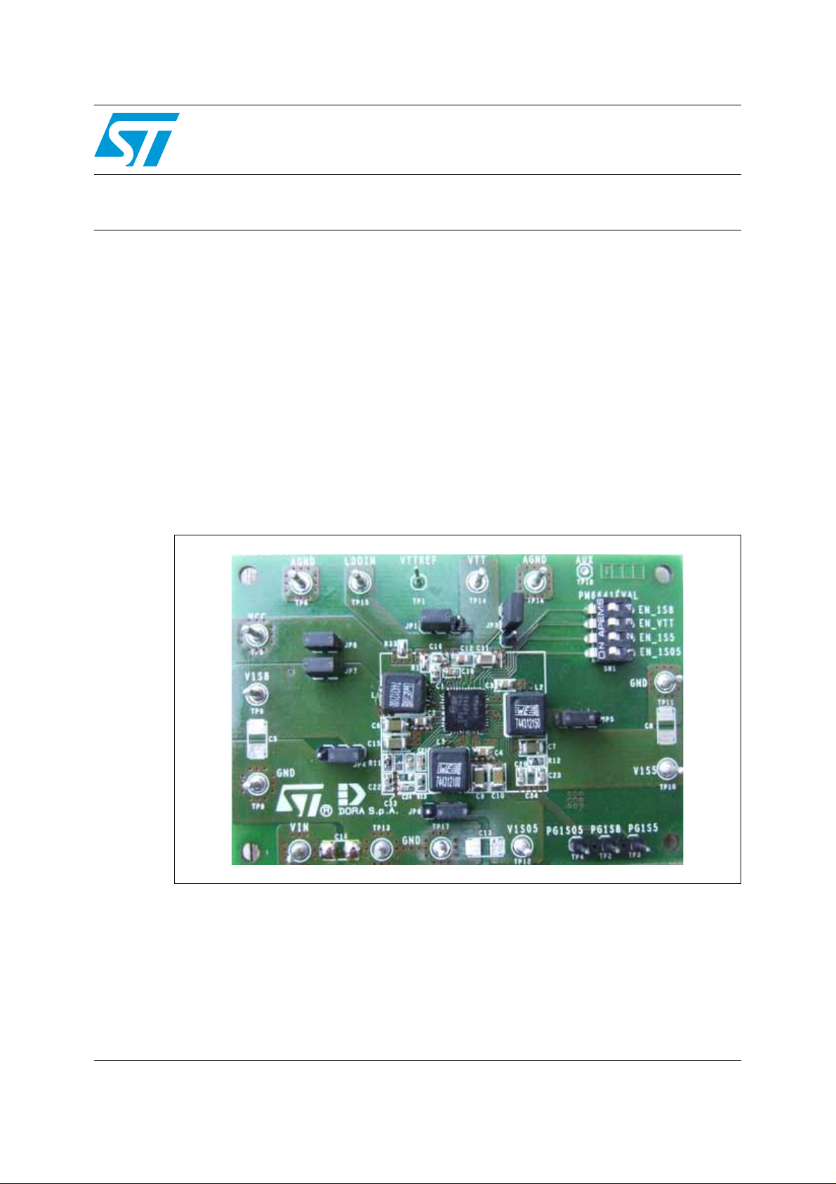
Figure 1. PM6641 demonstration board
September 2008 Rev 1 1/37
www.st.com
Page 2

Contents AN2787
Contents
1 Main features . . . . . . . . . . . . . . . . . . . . . . . . . . . . . . . . . . . . . . . . . . . . . . . 6
2 Demonstration kit schematic . . . . . . . . . . . . . . . . . . . . . . . . . . . . . . . . . . 7
3 Bill of material . . . . . . . . . . . . . . . . . . . . . . . . . . . . . . . . . . . . . . . . . . . . . . 8
4 Component assembly and layout . . . . . . . . . . . . . . . . . . . . . . . . . . . . . 10
5 I/O interface . . . . . . . . . . . . . . . . . . . . . . . . . . . . . . . . . . . . . . . . . . . . . . . 13
6 Recommended equipment . . . . . . . . . . . . . . . . . . . . . . . . . . . . . . . . . . . 14
7 Configuration . . . . . . . . . . . . . . . . . . . . . . . . . . . . . . . . . . . . . . . . . . . . . . 15
7.1 JP1 VDDQ output discharge (DSCG pin) . . . . . . . . . . . . . . . . . . . . . . . . . 15
7.2 JP3 switching regulator phase control (SET_PH1 pin) . . . . . . . . . . . . . . 15
7.3 JP4 1.8 V (VDDQ) external/internal divider (VFB_1S8 pin) . . . . . . . . . . . 16
7.4 JP5 1.5 V external/internal divider (VFB_1S5 pin) . . . . . . . . . . . . . . . . . . 17
7.5 JP6 1.05 V external/internal divider (VFB_1S05 pin) . . . . . . . . . . . . . . . . 17
7.6 JP7 current limit (CSNS pin) . . . . . . . . . . . . . . . . . . . . . . . . . . . . . . . . . . 18
8 Test setup . . . . . . . . . . . . . . . . . . . . . . . . . . . . . . . . . . . . . . . . . . . . . . . . . 19
9 Getting started . . . . . . . . . . . . . . . . . . . . . . . . . . . . . . . . . . . . . . . . . . . . . 20
10 STEVAL-ISA050V1 evaluation tests . . . . . . . . . . . . . . . . . . . . . . . . . . . . 21
10.1 SW regulators turn-on (soft-start) . . . . . . . . . . . . . . . . . . . . . . . . . . . . . . 21
10.2 SW regulator - working mode . . . . . . . . . . . . . . . . . . . . . . . . . . . . . . . . . . 22
10.3 Load regulation . . . . . . . . . . . . . . . . . . . . . . . . . . . . . . . . . . . . . . . . . . . . 25
10.4 Load transient responses . . . . . . . . . . . . . . . . . . . . . . . . . . . . . . . . . . . . . 27
10.5 Efficiency . . . . . . . . . . . . . . . . . . . . . . . . . . . . . . . . . . . . . . . . . . . . . . . . . 29
10.6 Phase management . . . . . . . . . . . . . . . . . . . . . . . . . . . . . . . . . . . . . . . . . 29
10.7 Fault management (OVP, UVP, UVLO, thermal) . . . . . . . . . . . . . . . . . . . 30
10.8 SW regulators current limit . . . . . . . . . . . . . . . . . . . . . . . . . . . . . . . . . . . . 33
10.9 Soft-end . . . . . . . . . . . . . . . . . . . . . . . . . . . . . . . . . . . . . . . . . . . . . . . . . . 33
2/37
Page 3

AN2787 Contents
10.10 Thermal behavior . . . . . . . . . . . . . . . . . . . . . . . . . . . . . . . . . . . . . . . . . . . 35
11 Revision history . . . . . . . . . . . . . . . . . . . . . . . . . . . . . . . . . . . . . . . . . . . 36
3/37
Page 4

List of figures AN2787
List of figures
Figure 1. PM6641 demonstration board . . . . . . . . . . . . . . . . . . . . . . . . . . . . . . . . . . . . . . . . . . . . . . . 1
Figure 2. PM6641 demonstration board schematic. . . . . . . . . . . . . . . . . . . . . . . . . . . . . . . . . . . . . . . 7
Figure 3. Top side component placement . . . . . . . . . . . . . . . . . . . . . . . . . . . . . . . . . . . . . . . . . . . . . 10
Figure 4. Top view . . . . . . . . . . . . . . . . . . . . . . . . . . . . . . . . . . . . . . . . . . . . . . . . . . . . . . . . . . . . . . . 10
Figure 5. Layer 2 view . . . . . . . . . . . . . . . . . . . . . . . . . . . . . . . . . . . . . . . . . . . . . . . . . . . . . . . . . . . . 11
Figure 6. Layer 3 view . . . . . . . . . . . . . . . . . . . . . . . . . . . . . . . . . . . . . . . . . . . . . . . . . . . . . . . . . . . . 11
Figure 7. Bottom view . . . . . . . . . . . . . . . . . . . . . . . . . . . . . . . . . . . . . . . . . . . . . . . . . . . . . . . . . . . . 12
Figure 8. Bottom side component placement . . . . . . . . . . . . . . . . . . . . . . . . . . . . . . . . . . . . . . . . . . 12
Figure 9. JP1 DSCG pin setting. . . . . . . . . . . . . . . . . . . . . . . . . . . . . . . . . . . . . . . . . . . . . . . . . . . . . 15
Figure 10. JP3 phase control. . . . . . . . . . . . . . . . . . . . . . . . . . . . . . . . . . . . . . . . . . . . . . . . . . . . . . . . 16
Figure 11. JP4 1.8 V divider selection . . . . . . . . . . . . . . . . . . . . . . . . . . . . . . . . . . . . . . . . . . . . . . . . . 16
Figure 12. JP5 1.5 V divider selection . . . . . . . . . . . . . . . . . . . . . . . . . . . . . . . . . . . . . . . . . . . . . . . . . 17
Figure 13. JP6 1.05 V divider selection . . . . . . . . . . . . . . . . . . . . . . . . . . . . . . . . . . . . . . . . . . . . . . . . 17
Figure 14. PM6641 demonstration board programmed current limit vs. CSNS resistor . . . . . . . . . . . 18
Figure 15. JP8 setting switching frequency . . . . . . . . . . . . . . . . . . . . . . . . . . . . . . . . . . . . . . . . . . . . . 18
Figure 16. PM6641 demonstration board test setup . . . . . . . . . . . . . . . . . . . . . . . . . . . . . . . . . . . . . . 19
Figure 17. VDDQ turn-on. . . . . . . . . . . . . . . . . . . . . . . . . . . . . . . . . . . . . . . . . . . . . . . . . . . . . . . . . . . 21
Figure 18. VDDQ, VTT and VTTREF turn-on . . . . . . . . . . . . . . . . . . . . . . . . . . . . . . . . . . . . . . . . . . . 22
Figure 19. PWM mode: VDDQ output voltage, phase voltage and inductor current, current
load = 2.3 A. . . . . . . . . . . . . . . . . . . . . . . . . . . . . . . . . . . . . . . . . . . . . . . . . . . . . . . . . . . . . 23
Figure 20. Pulse skip mode: VDDQ output vo ltage, phase voltage and inductor current, current
load = 0 A . . . . . . . . . . . . . . . . . . . . . . . . . . . . . . . . . . . . . . . . . . . . . . . . . . . . . . . . . . . . . . 24
Figure 21. Forced PWM mode (soft OV): VDDQ output voltage, phase voltage, inductor current
and Power Good signal . . . . . . . . . . . . . . . . . . . . . . . . . . . . . . . . . . . . . . . . . . . . . . . . . . . 24
Figure 22. VDDQ (1.8 V) load regulation . . . . . . . . . . . . . . . . . . . . . . . . . . . . . . . . . . . . . . . . . . . . . . . 25
Figure 23. 1.5 V load regulation. . . . . . . . . . . . . . . . . . . . . . . . . . . . . . . . . . . . . . . . . . . . . . . . . . . . . . 25
Figure 24. 1.05 V load regulation. . . . . . . . . . . . . . . . . . . . . . . . . . . . . . . . . . . . . . . . . . . . . . . . . . . . . 26
Figure 25. VTT load regulation . . . . . . . . . . . . . . . . . . . . . . . . . . . . . . . . . . . . . . . . . . . . . . . . . . . . . . 26
Figure 26. VTTREF load regulation . . . . . . . . . . . . . . . . . . . . . . . . . . . . . . . . . . . . . . . . . . . . . . . . . . . 26
Figure 27. VDDQ, VTT and VTTREF, VDDQ load transient response, IVDDQ = 0 to
2.3 A at 2.5 A/µs . . . . . . . . . . . . . . . . . . . . . . . . . . . . . . . . . . . . . . . . . . . . . . . . . . . . . . . . . 27
Figure 28. 1.5 V output voltage and inductor current, 1.5 V rail load transient response,
1.5 V = 0 to 1.25 A at 2.5 A/µs . . . . . . . . . . . . . . . . . . . . . . . . . . . . . . . . . . . . . . . . . . . . . . 27
Figure 29. 1.05 V output voltage and inductor current, 1.05 V rail load transient response.
I1.05 V = 0 to 1.75 A at 2.5 A/µs. . . . . . . . . . . . . . . . . . . . . . . . . . . . . . . . . . . . . . . . . . . . . 28
Figure 30. VDDQ, VTTREF, VTT and VTT output current , VTT rail load transient response,
IVTT = –1 A to +1 A at 2.5 A/µs . . . . . . . . . . . . . . . . . . . . . . . . . . . . . . . . . . . . . . . . . . . . . 28
Figure 31. SW regulators efficiency . . . . . . . . . . . . . . . . . . . . . . . . . . . . . . . . . . . . . . . . . . . . . . . . . . . 29
Figure 32. SW regulators phases, 120 deg phase shift. SETPH1 pin tied to AGND. . . . . . . . . . . . . . 29
Figure 33. SW regulators phases, no phase shift - synchronous clock, SETPH1 pin tied to AVCC . . 30
Figure 34. VDDQ, VTT, VTTREF output voltage, VDDQ temporarily shorted to 3.3 V, output
overvoltage protection triggered. . . . . . . . . . . . . . . . . . . . . . . . . . . . . . . . . . . . . . . . . . . . . 30
Figure 35. VDDQ, VTT, VTTREF output volta ge and VDDQ inductor current, VDDQ feedback pin
temporarily shorted to GND, output undervoltage protection triggered . . . . . . . . . . . . . . . 31
Figure 36. VDDQ (1.8 V), 1.5 V, 1.05 V output voltage and AVCC input power supply, input
undervoltage lockout triggered . . . . . . . . . . . . . . . . . . . . . . . . . . . . . . . . . . . . . . . . . . . . . . 32
Figure 37. VDDQ (1.8 V), 1.5 V, 1.05 V and VTT rails output voltage, thermal shutdown triggered. . 32
Figure 38. 1.5 V rail output voltage, 1.5 V inductor current and output current, peak current limit
4/37
Page 5

AN2787 List of figures
reached. . . . . . . . . . . . . . . . . . . . . . . . . . . . . . . . . . . . . . . . . . . . . . . . . . . . . . . . . . . . . . . . 33
Figure 39. VDDQ(1.8 V), VTT and VTTREF rail output voltage, EN_1S8 and EN_VTT tied to
AGND - soft off with tracking discharge . . . . . . . . . . . . . . . . . . . . . . . . . . . . . . . . . . . . . . . 34
Figure 40. VDDQ(1.8 V), VTT and VTTREF rail output voltage. EN_1S8 and EN_VTT tied to
AGND - soft off without tracking discharge. . . . . . . . . . . . . . . . . . . . . . . . . . . . . . . . . . . . . 34
Figure 41. PM6641 demonstration board surface temperature when loaded with typical currents,
T
= 23 °C, VIN = 3.3 V, FSW = 660 kHz. . . . . . . . . . . . . . . . . . . . . . . . . . . . . . . . . . . . . 35
amb
5/37
Page 6

Main features AN2787
1 Main features
Switching section
● 0.8 V ±1% voltage reference
● 2.7 V to 5.5 V input voltage range
● Fast response, constant frequency, current mode control
● Three independent, adjustable, SMPS for DDR2/3 (VDDQ) and chipset supply
● S3-S5 states compliant with DDR2/3 section
● Active soft-end for all outputs
● Selectable tracking discharge for VDDQ
● Separate Power Good signals
● Pulse skipping at light load
● Programmable current limit and soft-start for all outputs
● Latched OVP, UVP protection
● Thermal protection
Reference and termination voltages (VTTREF and VTT)
● ±2 Apk LDO for DDR2/3 termination (VTT) with foldback
● Remote VTT output sensing
● High-Z VTT output in S3
● ±15 mA low-noise DDR2/3 buffered reference (VTTREF)
6/37
Page 7
AN2787 Demonstration kit schematic
2 Demonstration kit schematic
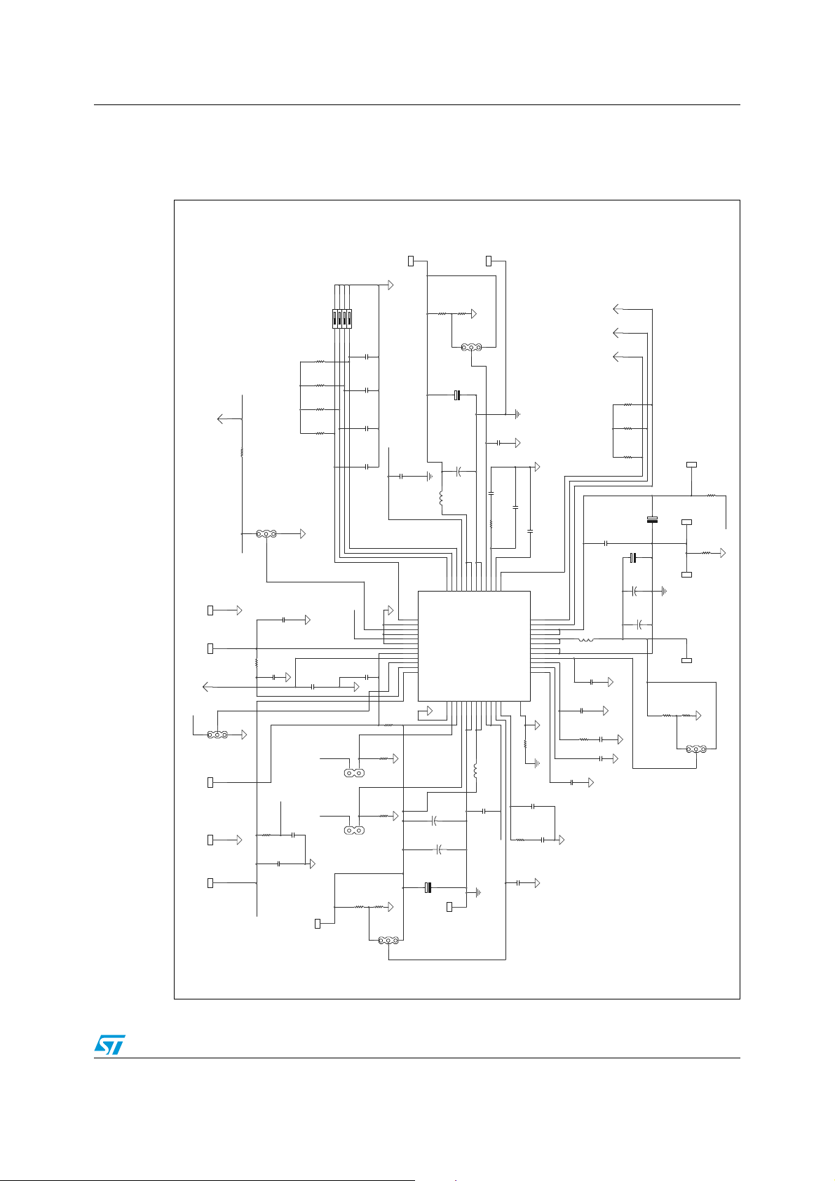
Figure 2. PM6641 demonstration board schematic
1
TP10
VOUT_1S5
678
SW1
SW DIP-4
123
4 5
0603-100p
R23
AUX
R22
AUX
1
TP18
AUX
R34
0603-join
JP3
STRIP 3
2
AVCC
1
TP16
AGND
1
TP14
VTT
R2
0603-4R3
1
TP1
VTTREF
2
AVCC
JP1
STRIP 3
1
TP15
LDOIN
1
TP6
AGND
1
TP5
VCC
C17
1 3
R1
0603-4R3
C1
VCC
R21
R20
1 3
C11
1206-22u
2
1
0603-100n
0603-33n
C18
AVCC
0603-100n
C16
0603-1u
TP9
VOUT_1S8
C28
0603-68k
0603-68k
0603-68k
0603-68k
1
0603-100p
C27
0603-100p
C26
0603-100p
C25
VIN
AVCC
C12
0805-10u
R33
0603-join
R4
AVCC
JP8
AVCC
JP7
0603-68k
1
2
STRIP 2
R3
0603-100k
1
2
STRIP 2
R5
0603-150k
R6
0603-120k
JP4
STRIP 3
2
R7
0603-100kR80603-120k
+
12
C3
0805-10u
2839-1u5
L2
1 2
35
EN_VTT36EN_1S5
EN_1S8
37
AGND_3
38
SET_PH1
39
AGND_2
40
AVCC
41
VTT_GND
42
VTT
43
LDO_IN
44
VTTREF
45
DSCG
46
VTT_FB
47
VCC
48
AGND_11SET_SWF2VOUT_1S83CSNS4SGND_1S8_15SGND_1S8_26VSW_1S8_17VSW_1S8_28VIN_1S8_19VIN_1S8_210VFB_1S811COMP_1S8
C15
B Case - 220u
C6
B Case - 220u
C5
EL SMD C-10u
+
12
TP8
GND
1 3
1
TP11
GND
1
TP4
PG_1S05
1
JP5
STRIP 3
1 3
2
C8
EL SMD C-10u
0603-100p
C30
C7
B Case - 220u
C23
0603-470p
C34
0603-15p
R12
0603-47k
29
33
34
28
31
VIN_1S5
EN_1S05
VSW_1S5_232VSW_1S5_1
SGND_1S5_230SGND_1S5_1
U1
PM6641_QFPN
2839-1u
L1
1 2
C2
1
C20
0603-22n
27
25
26
SS_1S5
PG_1S5
VFB_1S5
COMP_1S5
PG_1S8
24
PG_1S05
23
VIN_1S05_2
22
VIN_1S05_1
21
VSW_1S05_2
20
VSW_1S05_1
19
SGND_1S05_2
18
SGND_1S05_1
17
VFB_1S05
16
COMP_1S05
15
SS_1S05
14
SS_1S8
13
THER MAL
12
49
R32
0603-join
0603-15p
C32
0805-10u
VIN
R11
0603-100k
C22
0603-330p
0603-100p
C29
TP2
PG_1S8
1
TP3
PG_1S5
R19
0603-68k
AUX
R18
0603-68k
R17
0603-68k
TP7
VIN
1
R30
0603-join
12
+
C14
EL SMD C-10u
VIN
C4
0805-10u
C13
+
12
2839-1u
L3
1 2
0603-100p
C31
0603-15p
C33
R13
0603-68k
C24
0603-330p
C21
0603-22n
C19
0603-22n
TP17
EL SMD C-10u
TP13
C10
B Case - 220u
C9
B Case - 220u
TP12
R9
0603-56k
VCC
GND
1
R31
0603-join
1
GND
1
VOUT_1S05
R10
0603-180k
JP6
STRIP 3
1 3
2
7/37
Page 8
Bill of material AN2787
3 Bill of material
Table 1. PM6641 demonstration board list of components
Qty Component Description Package Part number MFR Value Note
1C1
C2, C3, C4,
4
4
5
1C11
2 C16, C17
1C18
3
2 C22, C24
1C23
4
C12
C5, C8, C13,
C14
C6, C7, C9,
C10, C15
C19, C20,
C21
C25, C26,
C27, C28
Ceramic, 10 V,
X5R, 20%
Ceramic, 10 V,
X5R, 20%
Ceramic, 4 V,
X5R, 20%
Ceramic, 6.3 V,
X5R, 10%
Ceramic, 16 V,
X7R, 10%
Ceramic, 25 V,
X7R, 10%
Ceramic, 16 V,
X7R, 10%
Ceramic, 50 V,
C0G, 5%
Ceramic, 50 V,
C0G, 5%
Ceramic, 50 V,
C0G, 5%
SMD 0603 Standard 1 µ
SMD 0805 GRM21BR61A106KE19 Murata 10 µ
SMD C case n.m.
SMD 1206 AMK316BJ107ML Taiyo Yuden 100 µ
SMD 1206 GRM31CR60J226KE19 Murata 22 µ
SMD 0603 Standard 100 n
SMD 0603 GRM188R71E333KA01 Murata 33 n
SMD 0603 Standard 22 n
SMD 0603 Standard 330 pF
SMD 0603 Standard 470 pF
SMD 0603 Standard 100 pF
C29, C30,
3
3
2R1, R2
1R3
9
1R16
1R5
8/37
C31
C32, C33,
C34
R4, R13
R17, R18,
R19, R20,
R21, R22,
R23
Ceramic, 50 V,
C0G, 5%
Ceramic, 50 V,
C0G, 5%
Chip resistor,
0.1 W, 1%
Chip resistor,
0.1 W, 1%
Chip resistor,
0.1 W, 1%
Chip resistor,
0.1 W, 1%
Chip resistor,
0.1 W, 1%
SMD 0603 n.m.
SMD 0603 n.m.
SMD 0603 Standard 3R3
SMD 0603 Standard 100 k
SMD 0603 Standard 68 k
SMD 0603 n.m.
SMD 0603 Standard 150 k
Ω
Ω
Ω
Page 9
AN2787 Bill of material
Table 1. PM6641 demonstration board list of components (continued)
Qty Component Description Package Part number MFR Value Note
2R6, R8
1R7
1R9
1R10
1R11
1R12
R32, R33,
3
2 R30, R31
2 L1, L3
1L2
1 U1 IC VR - 48-pin VFQFPN 7x7 PM6641 STMicroelectronics
R34
Chip resistor,
0.1 W, 1%
Chip resistor,
0.1 W, 1%
Chip resistor,
0.1 W, 1%
Chip resistor,
0.1 W, 1%
Chip resistor,
0.1 W, 1%
Chip resistor,
0.1 W, 1%
Chip resistor,
0.1 W, 1%
Chip resistor,
0.1 W, 1%
SMT 11Arms,
9.5 mΩ
SMT 9 Arms,
10.5 mΩ
SMD 0603 Standard 120 k
SMD 0603 Standard 100 kΩ
SMD 0603 Standard 56 kΩ
SMD 0603 Standard 180 k
SMD 0603 Standard 100 kΩ
SMD 0603 Standard 47 kΩ
SMD 0603 Standard 0
SMD 0603 n.m.
SMD 2827 744312100 /LF Würth 1.0 µH
SMD 2827 744312150 /LF Würth 1.5 µH
Ω
Ω
Ω short
JP1, JP3,
5
JP4, JP5,
JP6
2 JP7, JP8 Header, 2-pin SIP2
TP1, TP2,
5
TP3, TP4,
TP18
TP5, TP6,
TP7, TP8,
TP9, TP10,
13
TP11, TP12,
TP13, TP14,
TP15, TP16,
TP17
1 SW1 Switch 4-SPST DIP-8 Standard
Header, 3-pin SIP3
Header, single
pin
Test point
9/37
Page 10
Component assembly and layout AN2787
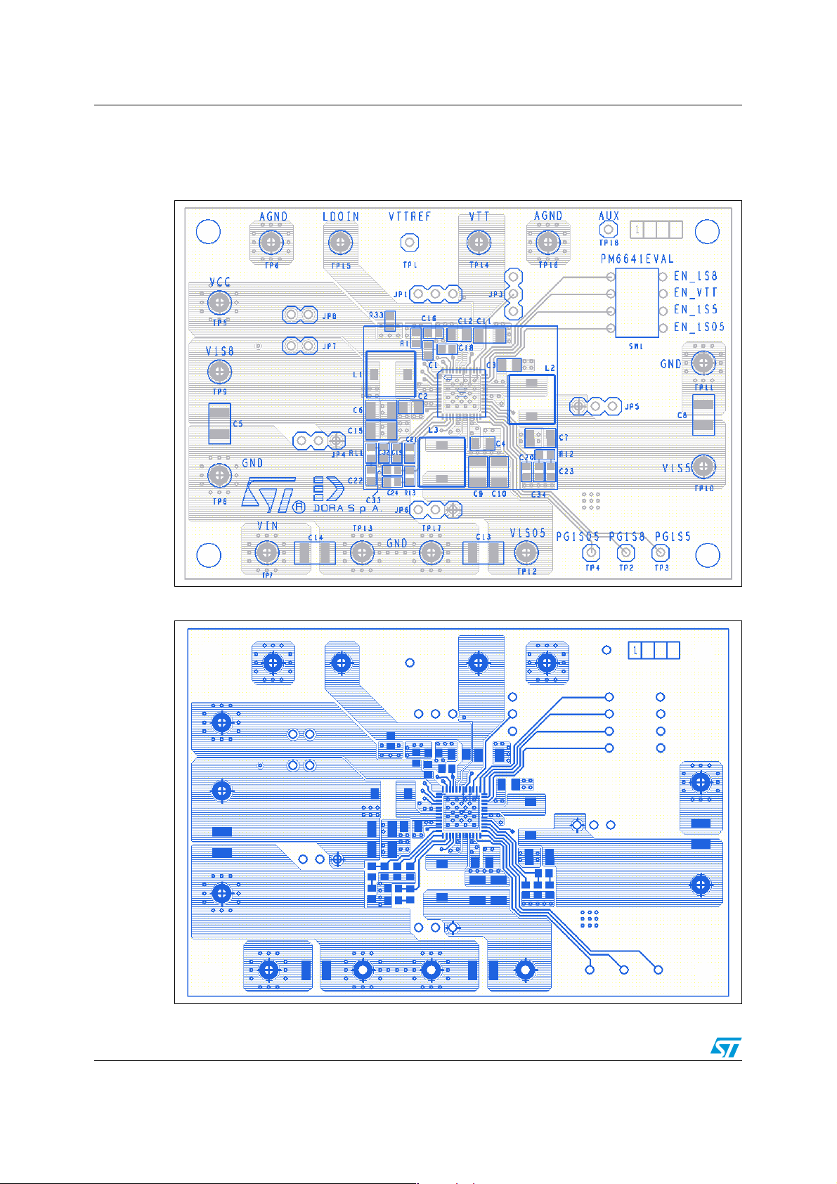
4 Component assembly and layout
Figure 3. Top side component placement
Figure 4. Top view
10/37
Page 11
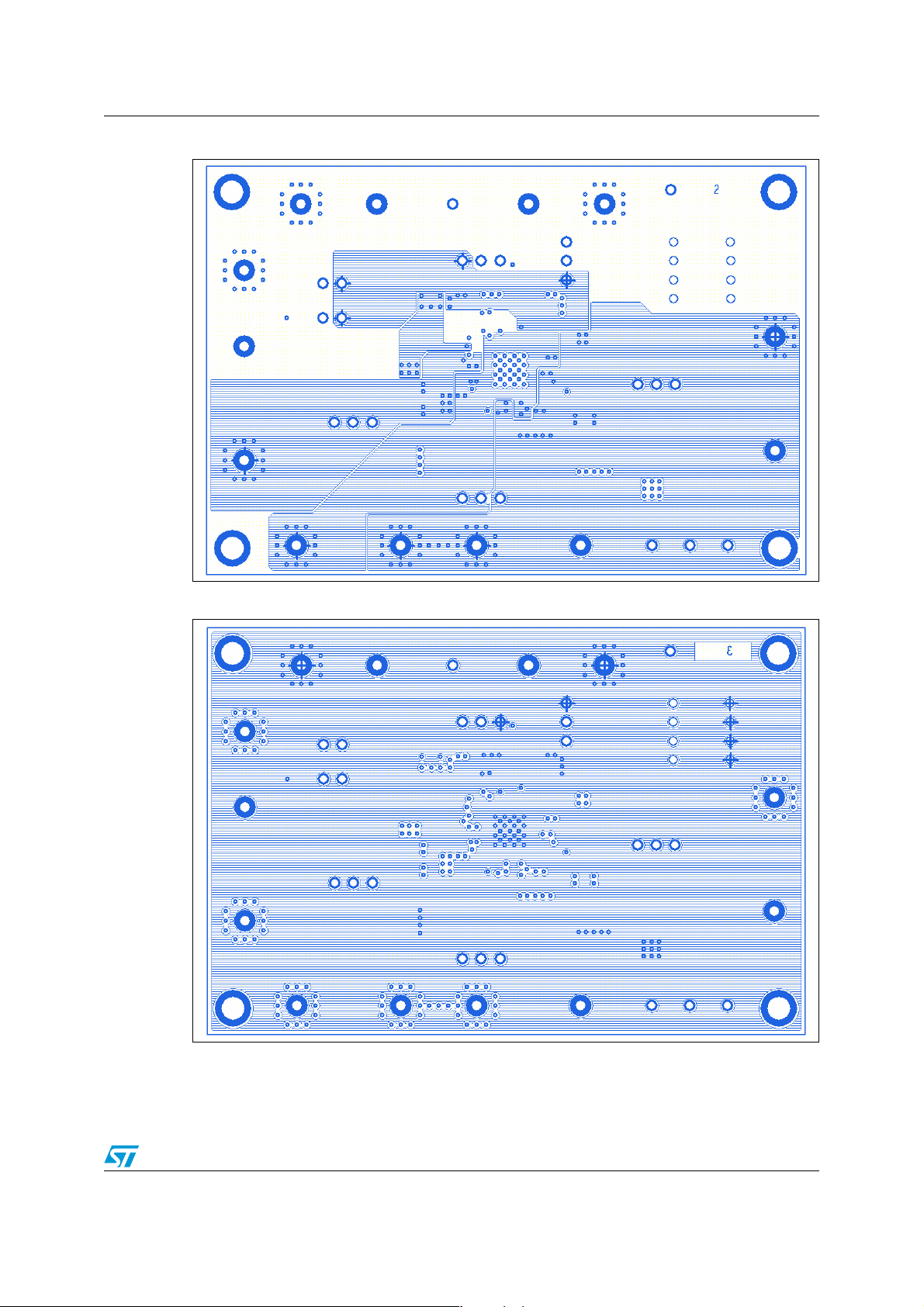
AN2787 Component assembly and layout
Figure 5. Layer 2 view
Figure 6. Layer 3 view
11/37
Page 12
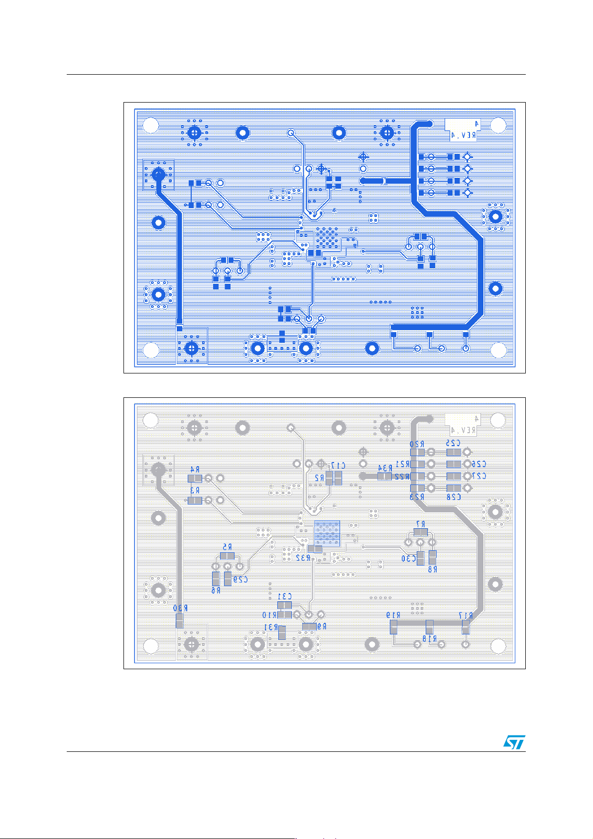
Component assembly and layout AN2787
Figure 7. Bottom view
Figure 8. Bottom side component placement
12/37
Page 13

AN2787 I/O interface
5 I/O interface
The PM6641 demonstration board has the following test points given in Table 2.
Table 2. PM6641 demonstration board input/output interface
Test point Description
VCC (TP5) +5 V IC supply, positive terminal
LDOIN (TP15) LDO (VTT) linear regulator input power supply
AUX (TP18) Auxiliary 3.3 V for pull-up (not required)
AGND (TP6, TP16) VCC, LDO, VTT and VTTREF common return
VIN (TP7) Power supply input voltage positive terminal
GND (TP8, TP11, TP13, TP17) Power supply and switching regulator outputs common return
V1S8 (TP9) 1.8 V (VDDQ) switching regulator output
V1S5 (TP10) 1.5 V switching regulator output
V1S05 (TP12) 1.05 V switching regulator output
VTT (TP14) LDO (VTT) linear regulator output
VTTREF (TP1) Voltage reference (VTTREF) buffer output
PG1S8 (TP2) 1.8 V (VDDQ) switching regulator Power Good signal
PG1S5 (TP3) 1.5 V switching regulator Power Good signal
PG1S05 (TP4) 1.05 V switching regulator Power Good signal
13/37
Page 14

Recommended equipment AN2787
6 Recommended equipment
● 5 V power supply
● 3.3 V, 20 W power supply
● Active loads
● Digital multimeters
● 500 MHz four-trace oscilloscope
14/37
Page 15

AN2787 Configuration
7 Configuration
The PM6641 demonstration board allows the user to test all the main features of the VR
PM6641, acting on 7 different jumpers and 4 switches . SW1 (4 SPST switches) lets the user
enable the switch ing regulators and the VTT linear regulator.
In the following sections each jumper is analyzed.
7.1 JP1 VDDQ output discharge (DSCG pin)
The JP1 jumper is used to choose between the trac king d ischarge or nontra c king discharge
of the 1.8 V rail (VDDQ) output.
When the 1.8 V rail is deactivated (EN_1S8 goes low) and the DSCG is set high, tracking
discharge takes place:
● The 1.8 V rail regulator is discharged by the internal MOSFETs
● The 0.9 V LDO and VTTREF work tracking with half of the 1.8 V rail
When the 0.9 V LDO and VTTREF reach a voltage threshold of about 300 mV, the
nontracking discharge mode is performed by closing the internal discharge MOSFETs.
If the nontracking discharge mode is chosen, when EN_1S8 goes low, the 1.8 V and 0.9 V
rails and the VTTREF buffer are independently discharged by internal MOSFETs.
Figure 9. JP1 DSCG pin setting
Tracking Discharge
Non Tracking Discharge
7.2 JP3 switching regulator phase control (SET_PH1 pin)
The JP3 jumper allows selecting two different oscillator settings in order to change the dela y
between the pulses that start the control cycle. The inner clock is divided in ord er to obtain
three slower clocks with a fixed delay of 120 deg. By setting JP3 as depicted in Figure 10, it
is possible to synchronize the 1.8 V, 1.5 V and 1.05 V switching regulator clocks or to select
120 deg delay in order to decrease the t otal RMS input current.
15/37
Page 16

Configuration AN2787
Figure 10. JP3 phase control
JP3
120deg Phase Shifting
Synchronous
The 120 deg phase shifting is the default configuration in which the inner clock is divided
and three pulses delayed by 120 deg are obtained to trigger the switching regulator loops.
The synchronous clocking allows all the regulat ors to start at the same pulse, avoiding the
jitter due to simultaneous turn-on and off of different sections, but increasing the overall
RMS input current.
7.3 JP4 1.8 V (VDDQ) external/internal divider (VFB_1S8 pin)
The JP4 jumper allows selecting the internal divider or the external divider for the 1.8 V
switching regulator . When the VFB_1S8 pin is connected d irectly to the output capacitor , the
internal divider is enabled and this section provides 1.8 V output voltage. When the
multifunction pin VFB_1S8 is tied to the central tap of an external divider, the switching
regulator becomes adjustable, with the following output voltage:
Equation 1
Vout
Figure 11. JP4 1.8 V divider selection
External Divider Enabled
Internal Divider Enabled
⎛
⎜
⎜
⎝
⎞
R
5
⎟
V8.01
⋅
+=
⎟
R
6
⎠
16/37
Page 17

AN2787 Configuration
7.4 JP5 1.5 V external/internal divider (VFB_1S5 pin)
The JP5 jumper allows selecting the internal divider or the external divider for the 1.5 V
switching regulator . When the VFB_ 1S5 pin is connected dire ctly to the output capacitor, the
internal divider is enabled and this section provides 1.5 V output voltage. When the
multifunction pin VFB_1S5 is tied to the central tap of an external divider, the switching
regulator becomes adjustable, with the following output voltage:
Equation 2
Vout
⎛
⎜
⎜
⎝
⎞
R
7
⎟
V8.01
⋅
+=
⎟
R
8
⎠
Figure 12. JP5 1.5 V divider selection
Internal Divider Enabled
External Divider Enabled
7.5 JP6 1.05 V external/internal divider (VFB_1S05 pin)
The JP6 jumper allows selecting the internal divider or the external divider for the 1.05 V
switching regulator. When the VFB_1S05 pin is connected directly to the output capacitor,
the internal divider is enabled and this section provides 1.05 V output voltage. When the
multifunction pin VFB_1S5 is tied to the central tap of an external divider, the switching
regulator becomes adjustable, with the following output voltage:
Equation 3
Vout
Figure 13. JP6 1.05 V divider selection
External Divider Enabled
Internal Divider Enabled
17/37
⎛
⎜
⎜
R
⎝
⎞
R
9
⎟
V8.01
⋅
+=
⎟
10
⎠
Page 18

Configuration AN2787
7.6 JP7 current limit (CSNS pin)
Each switching regulator current limit is set by inserting a resistor between the CSNS pin
and AGND. By changing this resistor value, all the current limits change, as shown in
Figure 14.
Figure 14. PM6641 demonstration board programmed current limit vs. CSNS
resistor
7,00
6,00
5,00
Peak Current Limit
4,00
3,00
Cur rent Limit [A]
2,00
1,00
0,00
50 70 90 110 130 150 170
Rcsns [kOhm]
CL_1V8
CL_1V5
CL_1V05
If the CSNS pin is tied to AVCC, the current limit is set through the inner reference resistor
(equal to 50 kΩ).
Figure 15. JP8 setting switching frequency
Default Switching Frequency
Adjusted Switching Frequency
18/37
Page 19

AN2787 Test setup
8 Test setup
Figure 16 shows the suggested setup connectio ns between the PM6641 demonstration
board, the loads, and the e xternal supply.
Figure 16. PM6641 demonstration board test setup
19/37
Page 20

Getting started AN2787
9 Getting started
The following step-by-step power-up and power-down sequences are provided in order to
correctly evaluate th e PM6641 demonstration board performance.
Power-up sequence
● Connect power supplies as shown in the PM6641 demonstration board test setup
(
Figure 16) and insert the meters in order to perform the desired performance
evaluation. Connect the scope-probes as desired
● Set the JP1 through JP8 jumpers in order to properly configure the PM6641
demonstration board. Set the SW1 switches (EN_1S8, EN_VTT, EN_1S5, EN_1S05)
to the ON position. Do not change jumper settings when the board is powered
● Set the VCC supply to 5 V ±5% and the current limit to 100 mA
● Set the VIN supply to a voltage in the range 2.7 V to 3.6 V
● Set all active loads to 0 A
● Tur n -on the VIN supply
● Tur n -on the VCC supply
● Vary the 1.8 V (VDDQ) load from 0 A to 4 A
● Vary the 1.5 V load from 0A to 2.5 A
● Vary the 1.05 V load from 0A to 3.5 A
● Vary the 0.9 V (VTT) load from 0 A to 2 A to test source capability. To test sink
capability use the alternative VTT load connection shown in
● Vary VTTREF load to test source capabilty.
Figure 16
Power-down sequence
● Decrease VTTREF and VTT loads to 0 A
● Turn-off the 1.8 V (VDDQ), 1.5 V, 1.05 V loads
● Decrease VCC supply from 5 V to 3.8 V in order to test the input undervoltage lockout
(UVLO)
● Increase VCC supply from 3.8 V to 5 V to restart the device
● Use the EN_1S8 and En_VTT switches to enter/exit the S0-S3-S5 states
● Tur n -off the VCC supply
● Tur n -off the VIN supply.
20/37
Page 21

AN2787 STEVAL-ISA050V1 evaluation tests
10 STEVAL-ISA050V1 evaluation tests
10.1 SW regulators turn-on (soft-start)
When the EN_xx pin is toggled high, the correspondent SW regulator perf orms the soft-start
as programmed through the external soft-start capacitor.
turn-on with C
Figure 17. VDDQ turn-on
SS
= 22 nF.
Figure 17 depicts VDDQ (1.8 V)
21/37
Page 22

STEVAL-ISA050V1 evaluation tests AN2787
Figure 18. VDDQ, VTT and VTTREF turn-on
10.2 SW regulator - working mode
Each switching regulator changes working mode wi th the appropriate load. When the load is
heavy, the SW enters PWM mode, but when the load is light, pulse skip mode is entered.
Each SW regulator is also able to sink current from the output (forced PWM mode when a
soft overvoltage occurs).
22/37
Page 23

AN2787 STEVAL-ISA050V1 evaluation tests
Figure 19. PWM mode: VDDQ output voltage, phase voltage and inductor current,
current load = 2.3 A
23/37
Page 24

STEVAL-ISA050V1 evaluation tests AN2787
Figure 20. Pulse skip mode: VDDQ output voltage, phase voltage and inductor
current, current load = 0 A
Figure 21. Forced PWM mode (soft OV): VDDQ output voltage, phase voltage,
inductor current and Power Good signal
24/37
Page 25

AN2787 STEVAL-ISA050V1 evaluation tests
10.3 Load regulation
Figure 22. VDDQ (1.8 V) load regulation
Figure 23. 1.5 V load regulation
25/37
Page 26

STEVAL-ISA050V1 evaluation tests AN2787
Figure 24. 1.05 V load regulation
Figure 25. VTT load regulation
Figure 26. VTTREF load regulation
26/37
Page 27

AN2787 STEVAL-ISA050V1 evaluation tests
10.4 Load transient responses
Figure 27. VDDQ, VTT and VTTREF, VDDQ load transient response, IVDDQ = 0 to
2.3 A at 2.5 A/µs
Figure 28. 1.5 V output voltage and inductor current, 1.5 V rail load transient
response, 1.5 V = 0 to 1.25 A at 2.5 A/µs
27/37
Page 28

STEVAL-ISA050V1 evaluation tests AN2787
Figure 29. 1.05 V output volta ge and inductor current, 1.05 V rail load transient
response. I
= 0 to 1.75 A at 2.5 A/µs
1.05 V
Figure 30. VDDQ, VTTREF, VTT and VTT output current, VTT rail load transient
response, I
= –1 A to +1 A at 2.5 A/µs
VTT
28/37
Page 29

AN2787 STEVAL-ISA050V1 evaluation tests
10.5 Efficiency
Figure 31. SW regulators efficiency
10.6 Phase management
Figure 32 and 33 show the SW regulators loaded with 1.3 A (VDDQ rail), 1.25 A (1.5 V rail)
and 1.75 A (1.05 V rail). By connecting the SETPH1 pin to AGND or to AVCC the following
two different phase shifts are allo wed.
Figure 32. SW regulators phases, 120 deg phase shift. SETPH1 pin tied to AGND
29/37
Page 30

STEVAL-ISA050V1 evaluation tests AN2787
Figure 33. SW regulators phases, no phase shift - synchronous clock, SETPH1 pin
tied to AVCC
10.7 Fault management (OVP, UVP, UVLO, thermal)
Each switching regulator is ab le to detect the output overvoltage and und ervoltage. When
the OV is detected th e high-side MOSFET is tu rned off and the lo w-side MO SFET is turned
on. When the UV is detected, the power MOSFETs are both turned off and the discharge
MOSFET is turned on (soft-end). The soft-end is also performed when the junction
temperature is higher than 150 °C.
Figure 34. VDDQ, VTT, VTTREF output voltage, VDDQ temporarily shorted to 3.3 V,
output overvoltage protection triggered
30/37
Page 31

AN2787 STEVAL-ISA050V1 evaluation tests
Figure 35. VDDQ, VTT, VTTREF output voltage and VDDQ inductor current, VDDQ
feedback pin temporaril y shorted to GND, output unde rvoltage pr otection
triggered
When the input undervoltage is detected, the VDDQ (1.8 V) rail performs the output voltage
soft-end. The 1.5 V and 1.05 V rails turn-off the high-side power MOSFET and turn-on the
low-side one.
31/37
Page 32

STEVAL-ISA050V1 evaluation tests AN2787
Figure 36. VDDQ (1.8 V), 1.5 V, 1.05 V output voltage and AVCC input power supply,
input undervoltage lockout triggered
Figure 37. VDDQ (1.8 V), 1.5 V, 1.05 V and VTT rails output voltage, thermal
shutdown triggered
32/37
Page 33

AN2787 STEVAL-ISA050V1 evaluation tests
10.8 SW regulators current limit
Cycle-by-cycle the high-side MOSFET current is monitored and if it's higher than the
programmed current limit, the high-side MOSFET is immediately turned off.
Figure 38. 1.5 V rail output voltage, 1.5 V inductor current and output current, peak
current limit reached
10.9 Soft-end
Each SW regulator , when turned off, performs the output voltage soft-en d by turning off the
power MOSFET and turning on the discharge MOSFET. When the output voltage is lower
than about 300 mV, the low-side power MOSFET is turned on. VTTREF and VTT can track
half of VDDQ also during the soft off.
These rails are allowed two different modes of discharge: tracking and nontracking
discharge.
33/37
Page 34

STEVAL-ISA050V1 evaluation tests AN2787
Figure 39. VDDQ(1.8 V), VTT and VTTREF rail output voltage, EN_1S8 and EN_VTT
tied to AGND - soft off with tracking discharge
Figure 40. VDDQ(1.8 V), VTT and VTTREF rail output voltage. EN_1S8 and EN_VTT
tied to AGND - soft off without tracking discharge
34/37
Page 35

AN2787 STEVAL-ISA050V1 evaluation tests
10.10 Thermal behavior
The device temperature is mainly influenced by LDO VTT current. The typical working
currents are shown in
Table 3. Average working currents for each rail
VTT is supplied by VDDQ and the de vice (average ) temperature is 54.5 °C.
Figure 41. PM6641 demonstration board surface temperature when loaded with
typical currents, T
Table 3.
Rail Current [A]
VDDQ (1.8 V) 1.35
1.5 V 1.25
1.05 V 1.75
VTT (0.9 V) 0.3
= 23 °C, V
amb
= 3.3 V, F
IN
= 660 kHz
SW
35/37
Page 36

Revision history AN2787
11 Revision history
Table 4. Document revision history
Date Revision Changes
05-Sep-2008 1 Initial release
36/37
Page 37

AN2787
Please Read Carefully:
Information in this document is provided solely in connection with ST products. STMicroelectronics NV and its subsidiaries (“ST”) reserve the
right to make changes, corrections, modifications or improvements, to this document, and the products and services described herein at any
time, without notice.
All ST products are sold pursuant to ST’s terms and conditions of sale.
Purchasers are solely res ponsibl e fo r the c hoic e, se lecti on an d use o f the S T prod ucts and s ervi ces d escr ibed he rein , and ST as sumes no
liability whatsoever relati ng to the choice, selection or use of the ST products and services described herein.
No license, express or implied, by estoppel or otherwise, to any intellectual property rights is granted under this document. If any part of this
document refers to any third pa rty p ro duc ts or se rv ices it sh all n ot be deem ed a lice ns e gr ant by ST fo r t he use of su ch thi r d party products
or services, or any intellectua l property c ontained the rein or consi dered as a warr anty coverin g the use in any manner whats oever of suc h
third party products or servi ces or any intellectual property contained therein.
UNLESS OTHERWISE SET FORTH IN ST’S TERMS AND CONDITIONS OF SALE ST DISCLAIMS ANY EXPRESS OR IMPLIED
WARRANTY WITH RESPECT TO THE USE AND/OR SALE OF ST PRODUCTS INCLUDING WITHOUT LIMITATION IMPLIED
WARRANTIES OF MERCHANTABILITY, FITNESS FOR A PARTICUL AR PURPOS E (AND THEIR EQUIVALE NTS UNDER THE LAWS
OF ANY JURISDICTION), OR INFRINGEMENT OF ANY PATENT, COPYRIGHT OR OTHER INTELLECTUAL PROPERTY RIGHT.
UNLESS EXPRESSLY APPROVED IN WRITING BY AN AUTHORIZED ST REPRESENTATIVE, ST PRODUCTS ARE NOT
RECOMMENDED, AUTHORIZED OR WARRANTED FOR USE IN MILITARY, AIR CRAFT, SPACE, LIFE SAVING, OR LIFE SUSTAINING
APPLICATIONS, NOR IN PRODUCTS OR SYSTEMS WHERE FAILURE OR MALFUNCTION MAY RESULT IN PERSONAL INJ URY,
DEATH, OR SEVERE PROPERTY OR ENVIRONMENTAL DAMAGE. ST PRODUCTS WHICH ARE NOT SPECIFIED AS "AUTOMOTIVE
GRADE" MAY ONLY BE USED IN AUTOMOTIVE APPLICATIONS AT USER’S OWN RISK.
Resale of ST products with provisions different from the statements and/or technical features set forth in this document shall immediately void
any warranty granted by ST fo r the ST pro duct or serv ice describe d herein and shall not cr eate or exten d in any manne r whatsoever , any
liability of ST.
ST and the ST logo are trademarks or registered trademarks of ST in various countries.
Information in this document su persedes and replaces all information previously supplied.
The ST logo is a registered trademark of STMicroelectronics. All other names are the property of their respective owners.
© 2008 STMicroelectronics - All rights reserved
STMicroelectronics group of compan ie s
Australia - Belgium - Brazil - Canada - China - Czech Republic - Finland - France - Germany - Hong Kong - India - Israel - Italy - Japan -
Malaysia - Malta - Morocco - Singapore - Spain - Sweden - Switzerland - United Kingdom - United States of America
www.st.com
37/37
 Loading...