

Page 1

AN2783
Application note
PM8800 demonstration kit for standard and high power PoE
PD interface and power supply, with auxiliary sources
Introduction
This document details the characteristics and performances of the PM8800 demonstration
kit which has been designed to cover a broad range of power over Ethernet (PoE)
applications. PM8800 is a highly integrated device embedding an IEEE802.3af compliant
powered device (PD) interface together with a PWM controller and support for auxiliary
sources.
Even though PM8800 can be configured to work in both isolated and non-isolated
topologies, this application note focuses on an isolated topology only, in two different output
power configurations (10 W and 20 W) and 2 different output voltages (5 V and 3.3 V).
The PM8800 demonstration kit supports diode as well as synchronous rectification.
Auxiliary sources can be connected to the board on 2 input points. One input allows
prevalence of the auxiliary sources with respect to the PoE, while the other input allows the
usage of a wall adaptor with voltage lower than the internal PoE UVLO threshold and still
benefits from the inherent inrush and DC current limit.
The above mentioned configurations are all supported by the PM8800 demonstration kit as
options on the same PCB. The bill of material (BOM) (see Section 5 on page 12) provides
the list of components to be mounted for each of the targeted configurations.
Figure 1. PM8800 demonstration kit
The high-power board appears on the left of the photo and standard board is on the right.
September 2008 Rev 2 1/47
www.st.com
Page 2

Contents AN2783
Contents
1 Main features . . . . . . . . . . . . . . . . . . . . . . . . . . . . . . . . . . . . . . . . . . . . . . . 6
2 Electrical specifications . . . . . . . . . . . . . . . . . . . . . . . . . . . . . . . . . . . . . . 7
3 Demonstration kit schematic . . . . . . . . . . . . . . . . . . . . . . . . . . . . . . . . . . 8
4 Board layout . . . . . . . . . . . . . . . . . . . . . . . . . . . . . . . . . . . . . . . . . . . . . . . . 9
4.1 Input/output connectors . . . . . . . . . . . . . . . . . . . . . . . . . . . . . . . . . . . . . . 11
4.2 Notes . . . . . . . . . . . . . . . . . . . . . . . . . . . . . . . . . . . . . . . . . . . . . . . . . . . . 11
5 Bill of material . . . . . . . . . . . . . . . . . . . . . . . . . . . . . . . . . . . . . . . . . . . . . 12
6 Power-up sequence . . . . . . . . . . . . . . . . . . . . . . . . . . . . . . . . . . . . . . . . . 16
7 Input section . . . . . . . . . . . . . . . . . . . . . . . . . . . . . . . . . . . . . . . . . . . . . . 17
7.1 Diode bridges . . . . . . . . . . . . . . . . . . . . . . . . . . . . . . . . . . . . . . . . . . . . . . 17
7.2 Input capacitors . . . . . . . . . . . . . . . . . . . . . . . . . . . . . . . . . . . . . . . . . . . . 17
7.3 Transient voltage suppression . . . . . . . . . . . . . . . . . . . . . . . . . . . . . . . . . 17
8 PoE section . . . . . . . . . . . . . . . . . . . . . . . . . . . . . . . . . . . . . . . . . . . . . . . 18
8.1 Signature . . . . . . . . . . . . . . . . . . . . . . . . . . . . . . . . . . . . . . . . . . . . . . . . . 18
8.2 Classification . . . . . . . . . . . . . . . . . . . . . . . . . . . . . . . . . . . . . . . . . . . . . . 18
8.3 UVLO and power-on . . . . . . . . . . . . . . . . . . . . . . . . . . . . . . . . . . . . . . . . . 19
8.4 Inrush current limit . . . . . . . . . . . . . . . . . . . . . . . . . . . . . . . . . . . . . . . . . . 19
8.5 DC current limit . . . . . . . . . . . . . . . . . . . . . . . . . . . . . . . . . . . . . . . . . . . . . 20
8.6 AUXI input . . . . . . . . . . . . . . . . . . . . . . . . . . . . . . . . . . . . . . . . . . . . . . . . 21
8.7 AUXII input . . . . . . . . . . . . . . . . . . . . . . . . . . . . . . . . . . . . . . . . . . . . . . . . 21
9 Power transformer and operating input voltage . . . . . . . . . . . . . . . . . . 22
10 Power converter . . . . . . . . . . . . . . . . . . . . . . . . . . . . . . . . . . . . . . . . . . . 23
10.1 Flyback continuous conduction mode . . . . . . . . . . . . . . . . . . . . . . . . . . . 23
10.2 Main switch current and current sensing . . . . . . . . . . . . . . . . . . . . . . . . . 24
10.3 Main switch power dissipation . . . . . . . . . . . . . . . . . . . . . . . . . . . . . . . . . 24
2/47
Page 3

AN2783 Contents
10.4 Rectifier diode dissipation . . . . . . . . . . . . . . . . . . . . . . . . . . . . . . . . . . . . 25
10.5 PM8800 internal power dissipation . . . . . . . . . . . . . . . . . . . . . . . . . . . . . 26
11 Layout guidelines . . . . . . . . . . . . . . . . . . . . . . . . . . . . . . . . . . . . . . . . . . 27
12 Test results . . . . . . . . . . . . . . . . . . . . . . . . . . . . . . . . . . . . . . . . . . . . . . . 29
12.1 Efficiency measurements . . . . . . . . . . . . . . . . . . . . . . . . . . . . . . . . . . . . . 29
12.2 5 V high-power board measurements . . . . . . . . . . . . . . . . . . . . . . . . . . . 31
12.3 3.3 V standard-power board measurements . . . . . . . . . . . . . . . . . . . . . . 36
12.4 IEEE 802.3af compatibility test . . . . . . . . . . . . . . . . . . . . . . . . . . . . . . . . . 42
Appendix A Schematic of high-power board . . . . . . . . . . . . . . . . . . . . . . . . . . . . 44
Appendix B Schematic of standard-power board . . . . . . . . . . . . . . . . . . . . . . . . 45
Revision history . . . . . . . . . . . . . . . . . . . . . . . . . . . . . . . . . . . . . . . . . . . . . . . . . . . . 46
3/47
Page 4

List of figures AN2783
List of figures
Figure 1. PM8800 demonstration kit . . . . . . . . . . . . . . . . . . . . . . . . . . . . . . . . . . . . . . . . . . . . . . . . . . 1
Figure 2. Demonstration kit schematic. . . . . . . . . . . . . . . . . . . . . . . . . . . . . . . . . . . . . . . . . . . . . . . . . 8
Figure 3. Assembly view: top and bottom layer . . . . . . . . . . . . . . . . . . . . . . . . . . . . . . . . . . . . . . . . . . 9
Figure 4. Top layer. . . . . . . . . . . . . . . . . . . . . . . . . . . . . . . . . . . . . . . . . . . . . . . . . . . . . . . . . . . . . . . 10
Figure 5. Inner layer 1 . . . . . . . . . . . . . . . . . . . . . . . . . . . . . . . . . . . . . . . . . . . . . . . . . . . . . . . . . . . . 10
Figure 6. Inner layer 2 . . . . . . . . . . . . . . . . . . . . . . . . . . . . . . . . . . . . . . . . . . . . . . . . . . . . . . . . . . . . 10
Figure 7. Bottom layer . . . . . . . . . . . . . . . . . . . . . . . . . . . . . . . . . . . . . . . . . . . . . . . . . . . . . . . . . . . . 11
Figure 8. Inrush current limit vs. RIRL . . . . . . . . . . . . . . . . . . . . . . . . . . . . . . . . . . . . . . . . . . . . . . . . 19
Figure 9. DC current limit vs. RDC. . . . . . . . . . . . . . . . . . . . . . . . . . . . . . . . . . . . . . . . . . . . . . . . . . . 20
Figure 10. Output power vs. VAUXII . . . . . . . . . . . . . . . . . . . . . . . . . . . . . . . . . . . . . . . . . . . . . . . . . . 22
Figure 11. 5 V out - standard board with diode rectification. . . . . . . . . . . . . . . . . . . . . . . . . . . . . . . . . 29
Figure 12. 5 V out - high-power board with synchronous rectification . . . . . . . . . . . . . . . . . . . . . . . . . 29
Figure 13. 3.3 V out - standard board with diode rectification . . . . . . . . . . . . . . . . . . . . . . . . . . . . . . . 30
Figure 14. 3.3 V out - high-power board with synchronous rectification . . . . . . . . . . . . . . . . . . . . . . . 30
Figure 15. Startup of the PM8800 demonstration kit with 5 V 1 A . . . . . . . . . . . . . . . . . . . . . . . . . . . . 31
Figure 16. Startup of the PM8800 demonstration kit with 5 V 4 A . . . . . . . . . . . . . . . . . . . . . . . . . . . . 31
Figure 17. Details of the inrush phase . . . . . . . . . . . . . . . . . . . . . . . . . . . . . . . . . . . . . . . . . . . . . . . . . 31
Figure 18. Details of the soft-start phase . . . . . . . . . . . . . . . . . . . . . . . . . . . . . . . . . . . . . . . . . . . . . . . 31
Figure 19. VDS and VGS of the primary MOSFET for 5 V 1 A . . . . . . . . . . . . . . . . . . . . . . . . . . . . . . 32
Figure 20. VDS and VGS of the primary MOSFET for 5 V 4 A . . . . . . . . . . . . . . . . . . . . . . . . . . . . . . 32
Figure 21. Details of the synchronous rectifier MOSFET voltage with 48 V and 4 A out . . . . . . . . . . 32
Figure 22. Output voltage ripple at 4 A output current . . . . . . . . . . . . . . . . . . . . . . . . . . . . . . . . . . . . . 33
Figure 23. Output voltage ripple at 4 A output current (1 sec persistence) . . . . . . . . . . . . . . . . . . . . . 33
Figure 24. Dynamic load 1 A to 4 A: output voltage (up) and output current (down) . . . . . . . . . . . . . 33
Figure 25. PM8800A response to a 6 A overload condition. . . . . . . . . . . . . . . . . . . . . . . . . . . . . . . . . 34
Figure 26. PM8800A recovering from a 6 A overload condition . . . . . . . . . . . . . . . . . . . . . . . . . . . . . 34
Figure 27. PM8800A response to a short on the load . . . . . . . . . . . . . . . . . . . . . . . . . . . . . . . . . . . . . 34
Figure 28. PM8800A recovering from a short on the load . . . . . . . . . . . . . . . . . . . . . . . . . . . . . . . . . . 34
Figure 29. Internal short on the secondary winding . . . . . . . . . . . . . . . . . . . . . . . . . . . . . . . . . . . . . . . 35
Figure 30. Switch between 48 V PoE and 24 V AUXII with 5 V at 2 A . . . . . . . . . . . . . . . . . . . . . . . . 35
Figure 31. back to 48 V removing the 24 V AUXII voltage with 5 V at 2 A . . . . . . . . . . . . . . . . . . . . . 35
Figure 32. Switch between 48 V PoE and 12 V AUXII with 5 V at 2 A . . . . . . . . . . . . . . . . . . . . . . . . 36
Figure 33. Back to 48 V removing the 12 V AUXII voltage with 5 V at 2 A . . . . . . . . . . . . . . . . . . . . . 36
Figure 34. Startup of the PM8800 demonstration kit with 3.3 V, 1 A . . . . . . . . . . . . . . . . . . . . . . . . . . 36
Figure 35. Startup of the PM8800 demonstration kit with 3.3 V, 3 A . . . . . . . . . . . . . . . . . . . . . . . . . . 36
Figure 36. Details of the inrush phase . . . . . . . . . . . . . . . . . . . . . . . . . . . . . . . . . . . . . . . . . . . . . . . . . 37
Figure 37. Details of the soft-start phase . . . . . . . . . . . . . . . . . . . . . . . . . . . . . . . . . . . . . . . . . . . . . . . 37
Figure 38. VDS and VGS of the primary MOSFET for 3.3 V 1 A . . . . . . . . . . . . . . . . . . . . . . . . . . . . . 37
Figure 39. VDS and VGS of the primary MOSFET for 3.3 V 3 A . . . . . . . . . . . . . . . . . . . . . . . . . . . . . 37
Figure 40. Details of the synchronous rectifier MOSFET voltage with 48 V and 3 A output current . . 38
Figure 41. Output voltage ripple at 3 A output current . . . . . . . . . . . . . . . . . . . . . . . . . . . . . . . . . . . . . 38
Figure 42. Output voltage ripple at 3 A output current (1 sec persistence) . . . . . . . . . . . . . . . . . . . . . 38
Figure 43. Dynamic load 1 to 3 A: output voltage (up) and output current (down) . . . . . . . . . . . . . . . 39
Figure 44. PM8800A response to a 5 A overload condition. . . . . . . . . . . . . . . . . . . . . . . . . . . . . . . . . 39
Figure 45. PM8800A recovering from a 5 A overload condition . . . . . . . . . . . . . . . . . . . . . . . . . . . . . 39
Figure 46. PM8800A response to a short on the load . . . . . . . . . . . . . . . . . . . . . . . . . . . . . . . . . . . . . 40
Figure 47. PM8800A recovering from a short on the load . . . . . . . . . . . . . . . . . . . . . . . . . . . . . . . . . . 40
Figure 48. Internal short on the secondary winding . . . . . . . . . . . . . . . . . . . . . . . . . . . . . . . . . . . . . . . 40
4/47
Page 5

AN2783 List of figures
Figure 49. Switch between 48 V PoE and 24 V AUXII with 3.3 V at 2 A . . . . . . . . . . . . . . . . . . . . . . . 41
Figure 50. Back to 48 V removing the 24 V AUXII voltage with 3.3 V at 2 A . . . . . . . . . . . . . . . . . . . . 41
Figure 51. Switch between 48 V PoE and 12 V AUXII with 3.3 V at 2 A . . . . . . . . . . . . . . . . . . . . . . . 41
Figure 52. Back to 48 V removing the 12 V AUXII voltage with 3.3 V at 2 A . . . . . . . . . . . . . . . . . . . . 41
Figure 53. Schematic of the 3.3/5 Vout high power with synchronous rectification . . . . . . . . . . . . . . . 44
Figure 54. Schematic of the 3.3/5 Vout standard power with diode rectification . . . . . . . . . . . . . . . . . 45
5/47
Page 6

Main features AN2783
1 Main features
The PM8800 demonstration kit has been designed to cover several PoE configurations with
easy customization.
● Basic configuration: (high-power applications)
– 5 V output
– Up to 4 A output
– 250 kHz operating switching frequency
– Flyback topology DCM/CCM
● Board size 70 x 90 mm
● Power Good indication
● Overall efficiency of 85% at full-load condition (Figure 12)
● Prevalence of the auxiliary source with respect to the PoE line (Section 8.7)
● 1500 Vrms isolation ensured by the power transformer
● Support for (see BOM options in Section 5):
– 5 V and 3.3V output
– diode or synchronous rectification
– standard IEEE802.3af or high-power applications
– non-isolated flyback topology
● Support for class 0-3 (IEEE802.3af) and class 4 (pre-standard modes)
The following 2 basic board configurations are addressed with the same PCB and referred
in the rest of the text as:
– Standard power: this configuration covers IEEE802.3af applications and it is
based on flyback topology with diode rectification.
– High power: this configuration targets applications with output power in excess of
the IEEE802.3af standard up to 20 W as output. This configuration is based on
flyback topology with synchronous rectification. The same configuration can be
used in PoE designs targeting high efficiency and/or with wide range auxiliary
input (down to 12 V with prevalence of the auxiliary with respect to PoE).
6/47
Page 7

AN2783 Electrical specifications
2 Electrical specifications
Table 1. Specifications
Parameter 10 W 20 W
VIN 30 V to 60 V at 10 W output 30 V to 60 V at 20 W output
Auxiliary VIN AUXI 18 V to 60 V 18 V to 60 V
Auxiliary VIN AUXII 12 V to 60 V 12 V to 60 V
VOUT
Peak-to-peak output
ripple
3.35 V +/- 100 mV at 3 A 3.35 V +/- 100 mV at 6 A
5.05 V +/- 100 mV at 2 A 5.05 V +/- 100 mV at 4 A
10 mVpp 20 mVpp
Efficiency DC-DC only
Overall efficiency
Switching frequency 250 kHz typ +/- 10% 250 kHz typ +/- 10%
Dynamic current step
Maximum overshoot 200 mV 400 mV
Maximum overshoot
time duration
Maximum undershoot 200 mV 400 mV
Maximum undershoot
time duration
Maximum DC test
current
Minimum DC test
current
83% typ at 3.3 V 3 A 86% typ at 3.3 V 6 A
87% typ at 5 V 2 A 88% typ at 5 V 4 A
78% typ at 3.3 V 3 A 81% typ at 3.3 V 6 A
81% typ at 5 V 2 A 84% typ at 5 V 4 A
1- 3 A max at 3.3 V 1- 6 A max at 3.3 V
1- 2 A max at 5 V 1- 4 A max at 5 V
200 ms 300 ms
200 ms 300 ms
3.5 A at 3.3 V 6.5 A at 3.3 V
2.5 A at 5 V 4.5 A at 5 V
00
7/47
Page 8

Demonstration kit schematic AN2783
g
g
g
k
k
k
k
k
n
y
y
g
k
k
M
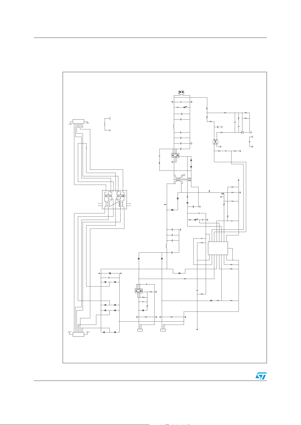
3 Demonstration kit schematic
Figure 2. Demonstration kit schematic
J5
1
2
DC OUTPU T
0.1u
C39
TP14
OUTOUTOUT
1k
R17
RJ45 D ata Jac
10
Chassis
1
234
1
2
4
5
12
13
T3
16
1
234
Chassis
10
RJ45 D at a and Po wer Jac
T
J2
9
Chassis
OUTPU
5
6
7
8
0
R1
0805
R7NM
6
M
R
N
6
3
7
89
H2019 / TLA-6T127LF
10
111415
567
8
Chassis
T
9
J1
INPU
Chassis
0
1206
R30
0805
C7NM0805
200V
Chassis
5
C6
200V
080
NM
0805
To be placed on sol der si de
Termination
123
4
5
6
T4
7
8
9
11
10
C5
R5
NM
NM
0805
0805
M
R4
N
C4
200V
NM
0805
0805
R3
NM
C3
NM
0805
0805
R2
C2
NM
NM
0805
0805
D3
SMAJ58 A
TP1
C1
0805
100V
0.1u
D24
SMA
4
STPS1H10 0
-
+
1
D2
3
A
SM
D22
STPS1H10 0
0
D20
SMA
4
STPS1H10
+
-
1
D1
3
A
STPS1H100SM
D18
ETH1-230LD
16
15
12
14
13
s
The H2019 footpri nt will be placed
NOTE f or dat aTr a nsf or me r
200V
e
Chassis
C8
1808
2KV
NM
200V
Termi na t i onTo be placed on solder sid
200V
TP 2
0
D25
SMA
2512
2512
STPS1H10
R9 N M
R8 N M
2
DF01S N M
SMA
D23
STPS1H10 0
SEE BO M
D21
SMA
STPS1H10 0
The resistors must be placed on
NOTE for 2512 Power Resis tors
2
DF01S N M
D19
STPS1H100SMA
solder side, belhind the SO8 body .
NOTE for Output Inductor
The 1206 footpri nt wil l be placed
The DPack footprint for the diode will be on top side.
NOTE for Output Recti er
T2
321
inside the FA2706 footprint
NOTE for Power Transf or mer
The 13P footprint will be placed
inside the E TH1-230LD one
D6
D4
SMC
STTH302 S
C41
0805
0.1u
100V
SO8
5
678
R12
Q1
4
STS10PF30L
3
1
2
330K
R10
0805
C27
0.1u
0
R5 0
BZX84C15
SOT23
3
1
D5
TP3
R11
15K
0805
1
2
3
J4
DC Power Jac k
AUX II
M
SEE BO
L
2
2
4
M
L2
L3 NM
N
R1
1206
0.33uH
between the inductor pad s
The Power SO8 footpr int of the mosfe t and the
4
SOD323
BAT46J NM
330K
0805
0.33uH
LPS401 2- 331
DO1813H-331ML
1
1
SEE BO M
5
8
6
7
470p
C11
0805
DPac
1
2
3
STPS15L30CB
7
2
D8
TP
15
R13
1206
Snubber on solder si de.
8910
7
COILCRAFT POE13P
SMC
STTH302 S
GND
TP5
TP4
1
DC Power Jac k
Q
143
SEE BO M
10
9
NM
T1
4
3
D10
5
C16NM080
TP6
R16NM1206
A
D9
SMAJ58
C17
1812
100V
2.2u
SEE BO M
2.2u
100V
C15
1812
2.2u
C14
100V
1812
2
L1
3.3uH
ME32 2 0 - 332 ML
1
C13
22u100V
8x10.2
D7
BAS21
K
R15
15
0805
2
3
J3
AUXI_IRL
TP8
N
NTR
TR
D11
Green LED
C24
330u
8x10.5
6.3V
1206
6.3V
10u
C23
C21
10u
1206
6.3V
C20
1206
6.3V
10u
9
C1
6.3V
10u
1206
C18
6.3V
10u
1206
4
3
D13
1
1
PowerSO 8
D12
STSJ60NH3LL
3
7118
12
5
1
2
6
R1 8
10
SMA
STPS1H100
D14
C25
BAT46J
SOD323
3.3k
R19
D15
GND
M
R49
N
SEE BO M
D26
SOT2 3
R23
10k
0
R25
0
R24
NM
R22
R26
BZX84C18
SOT23
SOT23
BZX84C18
NOTE
PowerSO8 footpr int wi ll be pl aced
on the solder side behi nd the DPac k one
COILCRAFT FA2706 - BL
TP10
0603
1u
16V
GND
C26
0.1u
Green LED
C34
0.1u
AGND
NM
C42
C28
0.1u
AGND
15
16
R21
AGND
88.7K
1%
RT
U1
1
RT
SS
%
21k
R32
1
10
1u
16V
C30
0603
NM
R34
R29
1
23
R41
Sharp PC3 H7
U2
D
4 1
AGN
R28
1k
C32
0.1u
M
C31
N
Q3A N M
PowerSO 8
8
7
6
2 3
5
1
6
4
R4
R40
SEE BO M
DPac k
STD22NM20L
Q3
3
2
TP11
BAT46J
SOD323
R39
1
D17 N
10
R38
R31
10 0805
100
R33
C33
1%
R44
12.4
M
M
1%
R47
N
1%
10
R43
SEE BO
M
22
C35
SEE BO
C37
4.7n
4
3
5
U3
TS431
SOT23-5
NM
1206
Those components will be plac ed
NOTE
GND
A
0
R42
TP1 2
1206
NM
1206
0.47 ohm
GND
1206
0.47 ohm
on the solder sid e
1812
2.2n
R2 0
NM
1206
C29
0
round that will be connected to th e
nal
470p
round plane close to pin 9 of PM880
D
D
D
G
GPnDGPn
G
G
P
P
P
P
GD
CS
VCC
GND
n
nD
n
nDG
13
14
9
10
12
11
CS
GD
VFB
VCC
GND
nPGD
PM8800
COMP
UXII
SS2A
3
4
I
I
X
XUAII
VIN
UA
HTSSO1 6
C36
0.1u NM
0805
Ex Pad
17
S
S
VIN
RCLAS
AUXI_IRL
DCCL
VS
6
5
7
8
VSS
DCC L
RCLASS
AUXI_IRL
100V
D27 NM
15k
1%
R37
1%
NM
0805
R35
GND po wer
NOTE
The AGND is a dedicated pla ne of si
A
SM
STPS1H100
V
C40
100p N M
R48
NM
D16
10k
R27
R36
SOD323
BAT46 J
TP9
TP13
NM
e is 50
is 0603 and tolera nce 5 %
is 0603 and the volta
NOTE for Ca paci tors
Where not indicated the bod
NOTE for Re sist ors
Where not indicated the bod
Sync Input
2KV
GND
AM01333v1
8/47
Page 9

AN2783 Board layout
4 Board layout
Figure 3. Assembly view: top and bottom layer
9/47
Page 10

Board layout AN2783
Figure 4. Top layer
Figure 5. Inner layer 1
Figure 6. Inner layer 2
10/47
Page 11

AN2783 Board layout
Figure 7. Bottom layer
4.1 Input/output connectors
In Figure 3 the main input / output connections of the reference board are presented:
● J1 is the RJ45 connector for the PoE input, with data and power applied through the
CAT5 cable (as an alternative, a positive voltage between 30 V and 60 V can be applied
to test points TP1 + and TP2 -)
● J2 is the RJ45 data output
● J3 is the power jack for AUXI input (as an alternative, the test points TP 3 + and TP4 -
can be used)
● J4 is the power jack for AUXII input (as an alternative, the test points TP5 + and TP9 -
can be used)
● J5 is the DC output connector
4.2 Notes
● Please note that the use of TP1 and TP2 limits the voltage polarity applied and that
these points are after the data transformer and diode bridges.
● AUXII is not protected against reverse polarity applied to it.
● For synchronization tests the capacitor C40 =100 pF must be mounted. Please take
care when using test point TP13 because this is a high impedance point that can easily
pick up noise from the board.
● Resistive or electronic loads can be used as loads. Limit the output capacitance
externally applied in order to not impact the loop compensation.
● As an input source a DC power supply with 60 V and 2 A capability is required.
● For auxiliary inputs a DC source of 60 V and 3 A capability is recommended.
11/47
Page 12

Bill of material AN2783
5 Bill of material
Table 2. Components for the 4 isolated configurations possible with the PM8800
Reference Description Pkg Manufacturer
5 V std power
3.3 V std power
3.3 V high power
Qty Qty Qty Qty
Printed circuit board
1 1 1 1 PM8800 eval kit
Capacitors
1 1 1 1 C1 Ceramic cap 0.1 µF 100 V 805 TDK
NM NM NM NM C36 Ceramic cap 0.1 µF 100 V 805 NM
NM NM NM NM C2, C7 Ceramic cap 200 V 805 NM
5 V high power
(1)
NM NM NM NM C8 Ceramic cap 2 kV 1812 NM
NM NM NM NM C9 Ceramic cap 805 NM
NM NM NM NM C10, C12 Ceramic cap 805 NM
1 1 1 1 C11 Ceramic cap 470 pF 50 V 805 Std
1 1 1 1 C13 Electrolytic cap 22 µF 100 V KX 8 x 10.2 SANYO
2 2 2 2 C14, C15 Ceramic cap 2.2 µF 100 V 1812 TDK
NM 1 NM 1 C17 Ceramic cap 2.2 µF 100 V 1812 TDK
NM NM NM NM C16 Ceramic cap 805 NM
2 2 NM NM C18, C19 Ceramic cap 10 µF 6.3 V 1206 TDK
3 3 NM NM
NM NM 2 2 C18, C19 Ceramic cap 10 µF 16 V 1206 TDK
NM NM 3 3
NM NM NM NM C22, C38 Ceramic cap 1206 NM
1 1 1 1 C24 Electrolytic cap 330 µF 6.3 V EX 8 x 10.5 SANYO
2 2 2 2 C25, C30 Ceramic cap 1 µF 16 V 603 TDK
5555
1 1 1 1 C29 Ceramic cap 2.2 nF 2 kV 1812 TDK
C20, C21,
C23
C20, C21,
C23
C26, C27,
C28, C34,
C39
Ceramic cap 10 µF 6.3 V 1206 TDK
Ceramic cap 10 µF 16 V 1206 TDK
Ceramic cap 0.1 µF 50 V 603 Std
NM NM NM NM C31 Ceramic cap 603 Std
1 1 1 1 C32 Ceramic cap 0.1 µF 50 V 603 Std
12/47
Page 13

AN2783 Bill of material
Table 2. Components for the 4 isolated configurations possible with the PM8800 (continued)
Reference Description Pkg Manufacturer
5 V std power
3.3 V std power
3.3 V high power
Qty Qty Qty Qty
1 1 1 1 C33 Ceramic cap 470 pF 50 V 603 Std
1 NM 1 NM C35 Ceramic cap 1 nF 50 V 603 Std
NM 1 NM 1 C35 Ceramic cap 22 nF 50 V 603 Std
1 1 1 1 C37 Ceramic cap 4.7 nF 50 V 603 Std
NM NM NM NM C40 Ceramic cap 100 pF 50 V 603 Std
1 1 1 1 C41 Ceramic cap 0.1 µF 100 V 805 TDK
Diodes
NM NM NM NM D1, D2 Diode bridge DF01S Dip Diodes
2 NM 2 NM D1A, D2A Diode bridge HD01 MiniDip Diodes
1 1 1 1 D3 Diode SMAJ58A SMA STMicroelectronics
5 V high power
2 2 2 2 D4, D7 Diode STTH302S SMC STMicroelectronics
1 1 1 1 D5 Diode Zener BZX84C15 SOT23 Std
NM NM NM NM D6 Diode BAT46J SOT323 STMicroelectronics
1 NM 1 NM D8 Diode STPS15L30CB DPACK - TO252 STMicroelectronics
1 1 1 1 D9 Diode SMAJ40A SMA STMicroelectronics
1 1 1 1 D10 Diode STPR120A SMA STMicroelectronics
2222 D11, D15
2 2 2 2 D12, D13 Diode Zener BZX84C18 SOT23 Std
1 1 1 1 D14 Diode BAT46J SOT323 STMicroelectronics
1 1 1 1 D16 Diode BAS316 SOT323 Std
NM NM NM NM D17 Diode BAT46J SOT323 STMicroelectronics
NM 8 NM 8 D18 : D25 Diode STPS1H100A SMA STMicroelectronics
NM 1 NM 1 D26 Diode BAS316 SOT323 Std
NM NM NM NM D27 STPS1H100A SMA STMicroelectronics
Connectors
2 2 2 2 J1, J2 Shielded RJ45 8-pole THT
2 2 2 2 J3, J4 DC power jack THT RAPC722 THT
1 1 1 1 J5 DC power connector 2-pole pitch 5.08
Diode green LED Toshiba
TLGE1100B
SMD Toshiba
Inductors
13/47
Page 14

Bill of material AN2783
Table 2. Components for the 4 isolated configurations possible with the PM8800 (continued)
Reference Description Pkg Manufacturer
5 V std power
3.3 V std power
3.3 V high power
Qty Qty Qty Qty
1 1 1 1 L1 Inductor 3.3 µH ME3220-332ML Coilcraft
5 V high power
1NM1NM L2
NM 1 NM 1 L3
MOSFETs
1 1 1 1 Q1 Mosfet STS10PF30L SO-8 STMicroelectronics
NM 1 NM 1 Q2 Mosfet STSJ60NH3LL PowerSO-8 STMicroelectronics
1 NM 1 NM Q3 Mosfet STD5N20L DPACK - TO252 STMicroelectronics
NM 1 NM 1 Q3 Mosfet STD22NM20M DPACK - TO252 STMicroelectronics
Resistors
1 1 1 1 R1 Resistor chip 0 Ω 805 Std
NM NM NM NM R2:R7, R35 Resistor chip 805 Std
NM NM NM NM R8, R9 Resistor chip 2.2 Ω 2512 Std
2 2 2 2 R11, R15 Resistor chip 15 kΩ 805 Std
1111 R10 Resistor chip 330 kΩ 805 Std
1 1 1 1 R12 Resistor chip 33 kΩ 805 Std
1111 R13 Resistor chip 15 Ω 1206 Std
NM NM NM NM
R14, R16,
R20, R41
Inductor 0.33 µH LPS4012-
331L
Inductor 0.33 µH DO1813H-
331ML
Resistor chip 1206 Std
Coilcraft
Coilcraft
1111 R17 Resistor chip 1 kΩ 603 Std
1111 R18 Resistor chip 10 Ω 603 Std
1 1 1 1 R19 Resistor chip 3K3 603 Std
1 1 1 1 R21 Resistor chip 88K7 1% 603 Std
NM NM NM NM
3333
2 2 2 2 R24, R25 Resistor chip 0 Ω 603 Std
1111 R26 Resistor chip 10 Ω 603 Std
1111 R28 Resistor chip 1 kΩ 603 Std
1111 R29 Resistor chip 1 kΩ 603 Std
14/47
R22, R34,
R36
R23, R27,
R38
Resistor chip 603 Std
Resistor chip 10 kΩ 603 Std
Page 15

AN2783 Bill of material
Table 2. Components for the 4 isolated configurations possible with the PM8800 (continued)
Reference Description Pkg Manufacturer
5 V std power
3.3 V std power
3.3 V high power
Qty Qty Qty Qty
1 1 1 1 R30 Resistor chip 0 Ω 1206 Std
1111 R31 Resistor chip 10 Ω 805 Std
1 1 1 1 R32 Resistor chip 21 kΩ 1% 603 Std
1 1 1 1 R33 Resistor chip 100 Ω 603 Std
NM 1 NM 1 R37 Resistor chip 15 kΩ 1% 603 Std
2 2 2 2 R39, R40 Resistor chip 0R47 1206 Std
NM NM NM NM R20, R41 Resistor chip 0 Ω 1206 Std
1 1 1 1 R42 Resistor chip 0 Ω 603 Std
1 1 1 1 R43 Resistor chip 10 kΩ 1% 603 Std
5 V high power
1 1 1 1 R44 Resistor chip 12K4 1% 603 Std
NM NM NM NM R46 Resistor chip 0R47 1206 Std
NM NM 1 1 R47 Resistor chip 15 kΩ 1% 603 Std
NM NM NM NM R48 Resistor chip 10 kΩ 1% 603 Std
1 NM 1 NM R49 Resistor chip 0 Ω 603 Std
1 1 1 1 R50 Resistor chip 0 Ω 603 Std
Transformers
NM 1 NM NM T1 Transformer EFD17 FA2706-BL Coilcraft
NM NM NM 1 T1 Transformer EFD17 FA2707-BL Coilcraft
1 NM NM NM T2 Transformer EP13 PoE13P-33L Coilcraft
NM NM 1 NM T2 Transformer EP13 PoE13P-50L Coilcraft
1NM1NM T3
Transformer H2019 / TLA-
6T127LF
Pulse/TDK
NM 1 NM 1 T4 Transformer ETH1-230LD Coilcraft
13 13 13 13 TP1:TP13 Test point 5013 Keystone
ICs
1 1 1 1 U1 PM8800 HTSSOP16 STMicroelectronics
1 1 1 1 U2 Optocoupler PC3H7 Sharp
1 1 1 1 U3 TSA431AILT SOT23-5 STMicroelectronics
1. PM8800 demonstration kit printed circuit board has been manufactured with the following Cu layer thicknesses:
Layer 1, 4: 35 µm (1 oz.) (top / bottom side)
Layer 2, 3: 35 µm (1 oz.) (power plane)
15/47
Page 16

Power-up sequence AN2783
6 Power-up sequence
It is recommended to apply power at the PoE input first, slowly increasing the voltage to
verify the absence of abnormal input current levels.
From 1.5 V to 11.5 V input, the signature phase, the PM8800 presents a 24.5 k
resistor as load.
After that in the range 11.5 V to 23 V, the classification phase, the PM8800 draws about 1.5
mA plus the current fixed with the classification resistance, if mounted.
After those two steps are verified, the voltage can be increased to 48 V typical.
Two green LEDs indicate proper operation of the PoE and DC/DC section of the PM8800
demonstration kit. D15 is the nPGD LED and is on when the internal hot-swap MOSFET is
closed, while D11 indicates the presence of the output voltage.
Ω nominal
16/47
Page 17

AN2783 Input section
7 Input section
7.1 Diode bridges
Two diode bridges are required at the input because PD must be able to accept voltage from
an Ethernet cable with undefined polarity and coming from either Tx and Rx or spare pairs.
Diode bridges must be at least 0.5 A to 1 A, 100 V . They contribute to increasing the
resistance presented by the PD to the PSE during the signature phase. For this reason the
internal signature resistance is set to 24.5 kΩ. Care must be taken to not exceed the
standard accepted values between 23.75 kΩ and 26.25 kΩ.
On the high-power board the diode bridges are replaced with discrete Schottky diodes, that
due to the lower voltage drop, allow lower losses at high output power.
7.2 Input capacitors
The IEEE802.3af standard requires a capacitor whose values are between 50 nF to 120 nF
during the signature phase and a minimum of 5 µF during the operating phase. A 100 nF,
100 V ceramic capacitor is used, placed near the VIN pin of PM8800.
In order to reduce the conducted emission, a C-L-C input filter has been designed with a
100 V aluminum capacitor at the input side, a 3.3 µH inductor and three 100 V ceramic
capacitors on the output side.
The resonant frequency of the filter is:
Equation 1
Freq
--------------------------------------- -=
2π LC
It has been selected to be about 5-10 times above the control loop bandwidth, to not impact
the stability of the control loop.
Equation 2
------------------------------------------------
C
≥
cer
8Fsw∆V
⋅⋅()
7.3 Transient voltage suppression
The PD in some circumstances (ringing, overshoot transients, static electricity, ground
differences, etc.) can see hundreds or thousands of volts at its RJ45 input connector. The
energy associated with these voltages can be quite large.
A transient voltage suppressor (TVS) is typically applied at the input of the PD, after the
diode bridge, in parallel to the 100 nF input capacitor.
1
⋅⋅()
cer
I
prms
ripple
The TVS must absorb this energy, but the PD interface must be designed to withstand an
additional 20 V or 30 V above the operating range until the TVS limits the voltage.
The TVS must be selected with a standoff voltage higher than the maximum voltage of 57 V
defined in the PoE standard which means a clamping voltage that can easily reach 100 V.
17/47
Page 18
PoE section AN2783
With the SMAJ58A the standoff is 58 V and the clamping voltage for a standard 10/1000 µs
transient is 93 V. PM8800 is able to withstand transient voltage up to 100 V without any
damage.
8 PoE section
8.1 Signature
Signature is the first phase in the PoE standard and allows a PSE (power source equipment)
to recognize the presence of a PD (powered device) that can accept power on the Ethernet
cable.
The PM8800 integrates a 24.5 kΩ resistance to simplify a standard PoE PD interface
design. Its value has been chosen to take into account the voltage drop across the diode
bridge and its effect on the effective resistor value presented at the RJ45 connector input.
This resistor is disconnected for input voltages higher than 11.5 V.
The required signature capacitance is obtained with C1= 100 nF, 100 V.
8.2 Classification
Classification is the second phase in the PoE standard and allows the PSE to allocate the
right amount of power for the PD connected on a single port.
The IEEE802.3af standard defines 4 power classes.
PM8800 has a dedicated pin for the classification resistor. The reference board has R35 left
open, corresponding to CLASS 0.
To select a different class please refer to the table below:
Table 3. RCLASS resistor value
CLASS PD power(W) R
0 0.44 -12.95 Open 0 4
1 0.44 - 3.84 158 9 12
2 3.84 - 6.49 82.5 17 20
3 6.49 - 12.95 52.3 26 30
4 Reserved 36.5 36 44
To provide a constant current during the classification phase, PM8800 has an internal
voltage regulator that maintains 1.4 V typ. across the classification resistor.
802.3af
classification current (mA)
(Ω)min. max
CLASS
The value of R35 is calculated taking into account the power consumption of PM8800 during
the classification phase, which is about 1.5 mA.
18/47
Page 19

AN2783 PoE section
R35 is disconnected at the end of the classification phase, when the input voltage rises
above 23 V.
8.3 UVLO and power-on
Power-on is the final state after successful detection and classification. The input voltage is
increased and an internal switch is closed to connect the PD load. The inrush current is
actively limited by the PM8800 itself.
The PM8800 is fully compliant with UVLO thresholds and inrush current limits defined in the
IEEE802.3af standard.
8.4 Inrush current limit
The inrush current in PM8800 has a three-step limit depending on the voltage across the
hot-swap MOSFET. The first two steps are fixed at 140 mA and 250 mA respectively, the
last step has a default value of 440 mA and it is programmable.
The external resistor to select the desired inrush current is found with the following formula:
Equation 3
R
kΩ[]
IRL
11200
----------------------- -=
I
IRL
mA[]
Figure 8. Inrush current limit vs. R
IRL
90
70
50
[kOhm]
IRL
R
30
10
100 150 200 250 300 350 400 450 500
I
[mA]
IRL
The PM8800 useful programming range for the inrush current limitation is between140 and
440 mA. The practical resistor value ranges between 25 kΩ and 82 kΩ.
Depending on the application, attention must be given to the choice of the inrush current
limit to avoid that the voltage drop on the external Ethernet cable causes UVLO conditions
during the charging phase of the bulk capacitor.
It is recommended to select this voltage drop (can be estimated as max: 20 Ω x I inrush) to
be lower than the UVLO hysteresis (7 Vmin) in order to avoid hiccup turn-on.
The inrush current is set to the default three-step values when the AUXI pin is pulled up over
the 2 V internal threshold by an auxiliary voltage.
19/47
Page 20

PoE section AN2783
Programming inrush current limit resistor R38 on the PM8800 reference board is left open,
thus the limits are set to the default values.
8.5 DC current limit
The continuous current limitation is internally set at 440 mA, but it is possible to modify it by
connecting a resistor between DCCL and VSS. This limitation is active after setting nPGD,
but in case the selected value is lower than the default inrush current, it also applies during
the inrush current phase.
The formula to select the desired DC current is the following:
Equation 4
11200
RDCkΩ[]
Figure 9. DC current limit vs. R
-----------------------=
mA[]
I
DC
DC
900
800
700
600
500
[mA]
DC
400
I
300
200
100
0
10 20 30 40 50 60 70 80
RDC [koh m]
The PM8800 useful programming range for the DC current limitation is between 150 mA and
800 mA. The practical resistor value ranges between 15 kΩ and 75 kΩ.
Please note that the DC current limit is not linked to the inrush current limit, both limits can
be set independently of each other.
Different current limits occur at different voltage drops between VSS and GND regardless of
the PM8800 operative phase:
● For a drop < 3 V, the DC limit occurs with a default value of 440 mA
● For a drop > 3 V but < 15 V, the 3rd step of inrush current occurs with a default value of
440 mA
● For a drop >15 V and < 30 V, the 2nd step of inrush current occurs with a default value
of 250 mA
● For a drop > 30 V, the 1st step of inrush current occurs with a default value of 140 mA
We suggest putting the DC limit over the inrush current which allows avoiding an increase of
current limiting during protection phases.
Programming DC current limit resistor R37 on the PM8800 standard reference board is left
open, leaving the default value as the limit, while a 15 kΩ is mounted on the high-power
version, putting the limit at 740 mA typ.
20/47
Page 21

AN2783 PoE section
8.6 AUXI input
The PM8800 reference board accepts auxiliary power sources applied before the hot-swap
MOSFET as low as 18 V (16 V seen at the pin VIN of device).
To do so and change the UVLO levels, the AUXI pin must be pulled up above 2 V with a
current greater than 70 µA.
The AUXI pin can be connected to the auxiliary voltage through a diode. In this case the
current flowing into the pin is internally limited to about 300 µA.
Depending on the output current drawn, the real operative AUXI voltage can be higher than
the above mentioned value, basically due to the DC current limitation which is maximum
input power at minimum applied on AUXI = 16V x 800 mA =12.8 W.
Another limitation on the operative AUXI voltage can be the power transformer, not designed
to work with a wide input voltage range for the maximum output power.
8.7 AUXII input
PM8800 can also accept auxiliary power sources applied after the hot-swap MOSFET as
slow as 12 V (9 V seen at the pins of device). In this case there is no current limitation and
an external circuit is recommended in order to limit the inrush current.
On the PM8800 reference board an active switch is implemented with a P-channel power
MOSFET, capable of limiting the inrush current at startup and with very low ohmic drop
during operation.
AUXII prevalence over PoE can be programmed forcing a current higher than 100µA in pin
AUXII of PM8800. In this case the PD is always powered from AUXII power source because
the interface circuits and the hot-swap MOSFET are forced in an off state. The pin can be
connected to the auxiliary voltage through a diode. In this configuration the current flowing
into the pin is internally limited to about 250 µA. AUXII can be conveniently used in case of
high-power PDs requiring input power higher than the 12.95 W specified in the IEEE802.3af
standard.
Please note that having the hot-swap MOSFET in an off state means having the IC
substrate in high impedance with GND. It is strongly recommended to move the signature
capacitor of 100 nF from the C1 position to C36. This capacitor is placed between VSS and
GND, implementing a low-impedance circuit at high frequency across the hot-swap
MOSFET, assuring a good HF connection of the IC substrate. The PM8800 reference board
is preset for AUXII prevalence over PoE, having R23 set to 10 kΩ.
Warning: In case of AUXII low input voltage sources, the condition
VIN < VCC must be avoided because of possible damage to
the device.
21/47
Page 22

Power transformer and operating input voltage AN2783
9 Power transformer and operating input voltage
The PM8800 demonstration kit can contain two different types of power transformers:
Table 4. Characteristics of the power transformer for the PM8800 evaluation kit
Type Lprimary N Ipeak sat Rsec
PoE13P-33L / 50L
FA2706-BL / 07-BL
127 µH
70 µH 6.8 / 4.85 3.5 A
6 / 4 1 A 24 mΩ/ 39 mΩ
8 mΩ/ 18.5 mΩ
The standard EP13 transformer is designed to operate at full IEEE802.3af power when the
input voltage is in the range 36-72 V. When working from auxiliary voltages lower than 36 V
the output power must be reduced in order to not saturate the transformer.
The custom transformer has been designed to work optimally over the full input range
between 12 V to 60 V in order to exploit the AUXII connection option made available by the
PM8800.
FA2706/7-BL can be also used to draw more power than 10 W when restricting the input
operational voltage range. For example about 20 W can be drawn with a minimum input
voltage of about 30 V, the minimum operating voltage of the PoE standard range.
Figure 10. Output power vs. VAUXII
Pout vs VAUXII wit h FA270x-BL
25
20
15
10
Pout ( W )
5
0
10 15 20 25 30 40 50 60
An auxiliary winding has been added in the FA2706/7-BL to directly drive a synchronous
power MOSFET as a secondary rectifier, in order to reduce the power losses associated
with a standard diode rectifier at high output currents.
When working at very low input voltage, as in the case of AUXII, the diode D6 can be added,
(actually not mounted on the reference board) to directly supply the VCC pin of PM8800.
Warning: In this condition please do not increase the AUXII voltage
above 15 V as permanent damage can occur to the device.
22/47
VAUXII ( V )
Page 23

AN2783 Power converter
10 Power converter
The PM8800 reference board implements a flyback converter operating in DCM
(discontinuous mode) at low output power and in CCM (continuous mode) for medium to
high output power.
The output secondary rectifier can be a classic diode for low to medium output power or a
synchronous rectifier for high output current.
Flyback configuration is the standard choice for a low-power isolated converter. It is the
simplest isolated converter, using the lowest number of power components.
CCM has been selected in order to reduce the stress on the power components, especially
on the secondary side.
CCM is assured only at medium to full output power, while in low output power the converter
works in DCM which allows reducing the size of the power transformer.
It is out of the scope of this document to show the whole flyback converter theory, which can
be found in every basic power supply handbook. In this application note we focus only on
the aspects directly related to the use of the PM8800 in a flyback converter.
10.1 Flyback continuous conduction mode
The flyback converter is in DCM when the energy stored during the ON phase has been
completely transferred to the secondary side during the OFF phase. This means that a
small period of time still remains during which no current is flowing on either side of the
power transformer.
When this period of time does not exist, i.e. when the energy stored has not been
completely transferred during the ON phase, the flyback is said to work in CCM.
Compared to CCM, DCM presents higher peak and rms current values on the primary
switch and on the output rectifier. This implies higher output ripple and require bigger input
and output filters.
CCM presents an RHP zero, which slightly complicates the control loop compensation. A
flyback converter designed to work in CCM is also stable in DCM.
The transfer function of a flyback in CCM is:
Equation 5
Vin Vds–()Ton⋅ Vout Vd+()NTswTon–()⋅⋅=
The above equation can be written as:
Equation 6
Vout Vd+()
------------------------------- -
Vin Vds–()
23/47
-------------------------- -=
N1D–()⋅
D
Page 24

Power converter AN2783
The maximum duty cycle can be obtained as:
Equation 7
Ton
max
--------------------
Tsw
------------------------------------------------------------------------------------=
Vin
min
N Vout Vd+()⋅
Vds–()N Vout Vd+()⋅+
10.2 Main switch current and current sensing
The current shape in the primary power switch is different when the flyback converter is
working in DCM or CCM. In DCM the shape is triangular with the current starting from zero,
while in CCM the shape is trapezoidal.
For CCM operations the peak current can be computed as:
Equation 8
Ipeak Ipave
∆I
L
--------+
-------------------------------------------- -
2
η N1D
Iout
–()⋅⋅
max
Vin
maxDmax
-----------------------------------------------------+==
Tsw⋅⋅
2Lp
which can be expressed as:
Equation 9
Ipeak
max
Pout
Vin Vds–()⋅⋅
--------------------------------------------------------- -
η D
Vin
maxDmax
-----------------------------------------------------+=
2Lp
Tsw⋅⋅
The RMS current can be:
Equation 10
2
∆I
L
L
---------- -+⋅
3
Iprms D
Ipeak2Ipeak
max
⎛⎞
–⋅=
⎜⎟
⎝⎠
∆I
--------
2
The above formula can be used to calculate the right current sense resistor, taking into
account that the first level of OCP is for PM8800 at 500 mV:
Equation 11
Rcs
500m V
----------------------------=
1.3 Ipeak⋅
The associated power dissipation on the sense resistor is:
Equation 12
Pcs Rcs Iprms
10.3 Main switch power dissipation
The power dissipation on the main power MOSFET is the sum of two terms:
24/47
2
⋅=
Page 25

AN2783 Power converter
Equation 13
Pswitching
Pcond Ron Iprms2D
Coss Vds2Fsw⋅⋅
------------------------------------------------ - Vds
⋅⋅=
2
max
max
Ipeak Tm Fsw⋅⋅⋅+=
where
Equation 14
Vds
max
1.2 Vin
Vspike is due to the leakage inductance of the power transformer and can be assumed to be
40 V max, as the snubber network on the primary side is built with a TVS with breakdown
voltage of 40 V.
Tm is the time to charge the Miller capacitor of the power MOSFET and can be estimated
as:
Equation 15
Tm
Note that if the major contribution to the MOSFET losses comes from the second term of the
switching power losses, the right choice is for a low gate charge power MOSFET.
10.4 Rectifier diode dissipation
The secondary output current is:
Equation 16
∆I
SL
Ispeak Isave
-----------+
2
Vspike+()NVoutVd+()⋅+[]⋅=
max
Qgd Rg⋅
-------------------------------- -=
Vcc Vgsth–
Iout
max
---------------------- -
1D
–
max
Vout Vd+()Tsw Ton–()⋅[]
-------------------------------------------------------------------------- -+==
Lp()N
⁄
2
2
∆I
SL
Isrms 1 D
–()Ispeak2Ispeak ∆I
max
SL
-----------+⋅–⋅=
3
The reverse voltage across the rectification diode is:
Equation 17
Vin
Vr
diode
max
------------------ - Vout+=
N
The power dissipated in the secondary diode, neglecting the reverse leakage losses, can be
estimated as:
Equation 18
P
diode
Isrms Vd 1 D
–()⋅⋅=
max
25/47
Page 26

Power converter AN2783
10.5 PM8800 internal power dissipation
A calculation must be done to verify that the PM8800 maximum junction temperature has
not been exceeded.
Major contributions to internal power dissipation are:
– startup circuit
– power MOSFET gate driver
– hot-swap MOSFET
– internal circuitry
It is strongly recommended to use an additional winding to generate an auxiliary VCC voltage of 9 V minimum, which switches off the internal startup circuit after the power-up of the
converter.
As mentioned before, the converter power MOSFET must be chosen as a good compromise
between low Ron and low total charge. The internal power dissipation associated to the gate
drive is:
Equation 19
P
drive
Vcc Qg Freq⋅⋅=
The hot-swap MOSFET dissipates internally:
Equation 20
P
hotswap
Ron Iin2⋅=
Internal power dissipation is due to circuits that draw current directly from VIN, like the hotswap controller or other logic circuits powered from VCC:
Equation 21
Typical operative values are I
P
device
= 5 mA and I
in
Vin Iin Vcc I iclog⋅+⋅=
= 3 mA.
logic
The total power dissipated by PM8800 is:
Equation 22
P
totPdrivePhotswapPdevice
++=
The following relationship must be satisfied:
Equation 23
T
ambPtot
where a typical value of Rth for PM8800 mounted on the ref board is 85 °C/W and Tjmax is
150 °C.
26/47
Rthja⋅ T<
+
jmax
Page 27

AN2783 Layout guidelines
11 Layout guidelines
We suggest the following guidelines for the layout of the PM8800:
● Place the component group including input ceramic capacitors, input side of
transformer, power MOSFET and sense resistors close to each other in order to keep
the interconnections as short as possible.
● Place the component group including secondary rectifier diode, output side of
transformer, output ceramic capacitors close to each other in order to keep the
interconnections as short as possible.
● Place the PM8800 in such a way as to have a short path to the gate of the power
MOSFET. Use a 20-30 mils wide path for this signal.
● Ground: there are basically 4 different grounds on the board (VSS, GND, RTN and
chassis ground).
– The exposed pad of PM8800 must be connected to VSS. Design a fill area with at
least 6 vias to the VSS plane. Try where possible to increase the number of VSS
power planes connected, at least below the PM8800 position, to improve the heat
dissipation of PM8800.
– GND must be divided into power gnd (to connect input caps, Rsense, PM8800 pin
9, AUXII circuitry, isolation cap) and signal gnd (to connect the other components
around the PM8800, the circuitry powered by VCC voltage, and the IC pin 16). The
signal gnd must be connected to power gnd in one point only, close to the PM8800
pin 9. Keep the power path on RTN (output side of transformer, secondary diode,
output connector) separated from the feedback network gnd, which is connected
only at the connector side.
● Design the power MOSFET area with at least 9-12 vias of connection to the internal
copper area. Try where possible to increase the number of power planes connected, at
least below the MOSFET position, to improve the heat dissipation.
● Design the secondary rectifier diode with at least 9-12 vias of connection to the internal
copper area.
● Try where possible to increase the number of power planes connected, at least below
the diode position, to improve the heat dissipation.
● Chassis: design copper areas on both side of the PCB. Do not place other grounds or
signals under the RJ45 and the data transformer area. Place any termination network
on the bottom side.
27/47
Page 28

Layout guidelines AN2783
More in detail:
Place the TVS close to the input diode bridges, if possible on the same side
1. Place the PM8800 and all the related components close to each other, use both sides
2. Place all the feedback components close to each other, use both sides
3. Place the sense resistors close to the power MOSFET, if possible on the same side
4. Place the input ceramic capacitors close to the input side of power transformer, if
possible on the same side
5. Place the primary snubber network close to the power transformer, on the bottom side
6. Place the rectifier diode close to the output side of the transformer, if possible on the
same side
7. Place the secondary snubber network close to the rectifier diode, bottom side
8. Place the output ceramic capacitors close to the rectifier diode and the power
transformer, on the copper areas, top side
9. Place the last ceramic capacitors close to the output terminal of the power connector,
bottom side
10. Place the 100 nF input capacitor close to the VSS and GND pins
11. Place the decoupling capacitors for VCC close to the relevant PM8800 pin
12. Place the components for RT and SS pins in a quiet area, separated as much as
possible from other signals
13. Use paths of at least 20 mils for signals connected to the IC pins 5,10,11
14. Connect the PM8800 pins 8,9,16 directly to the copper areas
15. Use a wide path or copper area for VIN, AUXI and AUXII networks
28/47
Page 29

AN2783 Test results
12 Test results
12.1 Efficiency measurements
Figure 11. 5 V out - standard board with diode rectification
90%
85%
80%
75%
Efficiency
70%
65%
60%
0.00 0.50 1.00 1.50 2.00 2.50
Iout [A]
5Vout DC-DC
5Vout Overall
Figure 12. 5 V out - high-power board with synchronous rectification
90%
85%
80%
75%
Efficiency
70%
5Vout HP DC-DC
65%
60%
0.0 0.5 1.0 1.5 2.0 2.5 3.0 3.5 4.0 4.5
Iout [A]
5Vout HP overall
29/47
Page 30

Test results AN2783
Figure 13. 3.3 V out - standard board with diode rectification
90%
85%
80%
75%
Efficiency
70%
65%
60%
0.0 0.5 1.0 1.5 2.0 2.5 3.0 3 .5
Iout [A]
3.3Vout DC-DC
3.3Vout overall
Figure 14. 3.3 V out - high-power board with synchronous rectification
90%
85%
80%
75%
Efficiency
70%
65%
60%
0.0 0.5 1.0 1.5 2.0 2.5 3.0 3.5 4.0 4.5 5.0 5.5 6.0 6.5
Iout [A]
3.3Vout HP DC-DC
3.3Vout HP overall
In the following pages are shown tests done on the 5 V high-power version and 3.3 V
standard version of the reference board.
Similar results and behaviors could be obtained with the 3.3 V high-power version and 5 V
standard versions.
30/47
Page 31

AN2783 Test results
12.2 5 V high-power board measurements
Figure 15. Startup of the PM8800
demonstration kit with 5 V 1 A
Figure 16. Startup of the PM8800
demonstration kit with 5 V 4 A
Ch1= output voltage, Ch2 = VSS voltage with respect to GND, Ch3 = VCC voltage, Ch4 =
input current
Figure 17. Details of the inrush phase Figure 18. Details of the soft-start phase
Ch1= output voltage, Ch2 = VSS voltage with respect to GND, Ch3 = VCC voltage (left) and
soft-start (right), Ch4 = input current.
31/47
Page 32

Test results AN2783
Figure 19. V
DS
and V
of the primary
GS
MOSFET for 5 V 1 A
Ch2 = primary side power MOSFET gate voltage, Ch3 = primary side power MOSFET drain
voltage.
Figure 21. Details of the synchronous rectifier MOSFET voltage with 48 V and 4 A
out
Figure 20. VDS and V
MOSFET for 5 V 4 A
of the primary
GS
Ch1 = secondary side power MOSFET drain-source voltage, Ch3 = primary side power
MOSFET drain voltage
32/47
Page 33

AN2783 Test results
Figure 22. Output voltage ripple at 4 A output
current
Figure 24. Dynamic load 1 A to 4 A: output voltage (up) and output current (down)
Figure 23. Output voltage ripple at 4 A output
current (1 sec persistence)
33/47
Page 34

Test results AN2783
Figure 25. PM8800A response to a 6 A
overload condition
Ch1 = output voltage, Ch2 = soft-start voltage, Ch3 = voltage across the hot-swap MOSFET,
Ch4 = input current.
Figure 27. PM8800A response to a short on
the load
Figure 26. PM8800A recovering from a 6 A
overload condition
Figure 28. PM8800A recovering from a short
on the load
Ch1 = output voltage, Ch2 = soft-start voltage, Ch3 = voltage across the hot-swap MOSFET,
Ch4 = input current.
34/47
Page 35

AN2783 Test results
Figure 29. Internal short on the secondary winding
Ch1 = output voltage, Ch2 = soft-start voltage, Ch3 = voltage across the hot-swap MOSFET,
Ch4 = input current
Figure 30. Switch between 48 V PoE and 24 V
AUXII with 5 V at 2 A
Ch1 = output voltage, Ch2 = internal primary voltage, Ch3 = voltage across the hot-swap
MOSFET, Ch4 = AUXII input current
Figure 31. back to 48 V removing the 24 V
AUXII voltage with 5 V at 2 A
35/47
Page 36

Test results AN2783
Figure 32. Switch between 48 V PoE and 12 V
AUXII with 5 V at 2 A
Figure 33. Back to 48 V removing the 12 V
AUXII voltage with 5 V at 2 A
Ch1 = output voltage, Ch2 = internal primary voltage, Ch3 = voltage across the hot-swap
MOSFET, Ch4 = AUXII input current
12.3 3.3 V standard-power board measurements
Figure 34. Startup of the PM8800
demonstration kit with 3.3 V, 1 A
Ch1= output voltage, Ch2 = VSS voltage with respect to GND, Ch3 = VCC voltage,
Ch4 = input current
Figure 35. Startup of the PM8800
demonstration kit with 3.3 V, 3 A
36/47
Page 37

AN2783 Test results
Figure 36. Details of the inrush phase Figure 37. Details of the soft-start phase
Ch1= output voltage, Ch2 = VSS voltage with respect to GND, Ch3 = VCC voltage (left) and
soft-start (right), Ch4 = input current
Figure 38. VDS and V
MOSFET for 3.3 V 1 A
of the primary
GS
Ch2 = primary side power MOSFET gate voltage, Ch3 = primary side power MOSFET drain
voltage
Figure 39. VDS and V
MOSFET for 3.3 V 3 A
of the primary
GS
37/47
Page 38

Test results AN2783
Figure 40. Details of the synchronous rectifier MOSFET voltage with 48 V and 3 A
output current
Ch1 = secondary side power MOSFET drain-source voltage, Ch3 = primary side power
MOSFET drain voltage
Figure 41. Output voltage ripple at 3 A output
current
Figure 42. Output voltage ripple at 3 A output
current (1 sec persistence)
38/47
Page 39

AN2783 Test results
Figure 43. Dynamic load 1 to 3 A: output voltage (up) and output current (down)
Figure 44. PM8800A response to a 5 A
overload condition
Ch1 = output voltage, Ch2 = soft-start voltage, Ch3 = voltage across the hot-swap MOSFET,
Ch4 = input current
Figure 45. PM8800A recovering from a 5 A
overload condition
39/47
Page 40

Test results AN2783
Figure 46. PM8800A response to a short on
the load
Ch1 = output voltage, Ch2 = soft-start voltage, Ch3 = voltage across the hot-swap MOSFET,
Ch4 = input current
Figure 48. Internal short on the secondary winding
Figure 47. PM8800A recovering from a short
on the load
Ch1 = output voltage, Ch2 = soft-start voltage, Ch3 = voltage across the hot-swap MOSFET,
Ch4 = input current
40/47
Page 41

AN2783 Test results
Figure 49. Switch between 48 V PoE and 24 V
AUXII with 3.3 V at 2 A
Ch1 = output voltage, Ch2 = internal primary voltage, Ch3 = voltage across the hot-swap
MOSFET, Ch4 = AUXII input current
Figure 51. Switch between 48 V PoE and 12 V
AUXII with 3.3 V at 2 A
Figure 50. Back to 48 V removing the 24 V
AUXII voltage with 3.3 V at 2 A
Figure 52. Back to 48 V removing the 12 V
AUXII voltage with 3.3 V at 2 A
Ch1 = output voltage, Ch2 = internal primary voltage, Ch3 = voltage across the hot-swap
MOSFET, Ch4 = AUXII input current
41/47
Page 42

Test results AN2783
12.4 IEEE 802.3af compatibility test
Additional tests of compatibility to the IEEE802.3af standard have been done with the
PDA100 PD tester from Sifos Technologies. Results obtained with the 5 V, 2 A standard
board are summarized inTab le 5, 6, and 7. All tests have been successfully completed.
Table 5. Compatibility test at -45 degC
Alt-A MDI Alt-A MDI-X Alt-B MDI Alt-B MDI-X
Det. resistance 25.18 kΩ 25.16 kΩ 25.25 kΩ 25.25 kΩ
Det. capacitance 0.109 µF 0.092 µF 0.109 µF 0.103 µF
Class. current 1.4 mA 1.4 mA 1.4 mA 1.4 mA
Class result 0 0 0 0
Average power 12.52 W 12.52 W 12.38 W 12.38 W
Max current 266.2 mA 261.6 mA 258.8 mA 258.6 mA
Min current 260.3 mA 260.3 mA 257.4 mA 257.3 mA
Av. current 261.0 mA 260.9 mA 258.0 mA 258.0 mA
Turn-on voltage 40.0 V 40.0 V 40.0 V 40.0 V
Turn-off voltage 33.9 V 33.9 V 33.1 V 33.1 V
Table 6. Compatibility test at room temperature
Alt-A MDI Alt-A MDI-X Alt-B MDI Alt-B MDI-X
Det. resistance 24.90 kΩ 24.99 kΩ 24.95 kΩ 25.09 kΩ
Det. capacitance 0.103 µF 0.104 µF 0.104 µF 0.109 µF
Class. current 1.4 mA 1.3 mA 1.3 mA 1.3 mA
Class result 0 0 0 0
Average power 12.53 W 12.53 W 12.34 W 12.34 W
Max current 266.2 mA 262.0 mA 257.7 mA 257.6 mA
Min current 260.7 mA 260.5 mA 256.8 mA 256.8 mA
Average current 261.1 mA 261.2 mA 257.2 mA 257.1 mA
Turn-on voltage 40.0 V 40.0 V 40.0 V 40.0 V
Turn-off voltage 34.2 V 34.1 V 33.1 V 33.0 V
Table 7. Compatibility test at +85 degC
Alt-A MDI Alt-A MDI-X Alt-B MDI Alt-B MDI-X
Det. resistance 25.47 kΩ 25.49 kΩ 25.54 kΩ 25.57 kΩ
Det. capacitance 0.114 µF 0.112 µF 0.109 µF 0.103 µF
Class. current 1.3 mA 1.3 mA 1.3 mA 1.3 mA
Class result 0000
Average power 12.59 W 12.59 W 12.36 W 12.37 W
42/47
Page 43

AN2783 Test results
Table 7. Compatibility test at +85 degC (continued)
Alt-A MDI Alt-A MDI-X Alt-B MDI Alt-B MDI-X
Max current 267.2 mA 263.0 mA 258.6 mA 258.6 mA
Min current 261.8 mA 261.8 mA 257.4 mA 257.2 mA
Average current 262.3 mA 262.4 mA 257.7 mA 257.8 mA
Turn-on voltage 39.8 V 39.7 V 39.7 V 39.7 V
Turn-off voltage 34.1 V 34.1 V 32.9 V 32.9 V
43/47
Page 44
Schematic of high-power board AN2783
Appendix A Schematic of high-power board
Figure 53. Schematic of the 3.3/5 Vout high power with synchronous rectification
J5
J5
1
1
2
2
DC OUTPU T
DC OUTPU T
C39
0.1u
C39
0.1u
TP14
TP14
OUTOUTOUT
OUTOUTOUT
1k
1k
R17
R17
RJ45 Data Jack
RJ45 Data Jack
J2
J2
10
10
9
9
23456
23456
Chass is
Chass is
OUTPUT
OUTPUT
7
8
7
8
0
0
R1
R1
0805
0805
Chass is
Chass is
1
1
T4
T4
7
7
8
8
TP1
TP1
Chass is
Chass is
0
0
1206
1206
R30
R30
6
6
9
9
1011121314
1011121314
D3
D3
SMAJ58A
SMAJ58A
C1
0.1u
0805
C1
0.1u
0805
D24
D24
SMA
SMA
STPS1H 10 0
STPS1H 10 0
D22
STPS1H100
SMA
D22
STPS1H100
SMA
D20
D20
SMA
SMA
STPS1H 10 0
STPS1H 10 0
2
2
L3
L3
0.33uH
0.33uH
DO1813H-331ML
DO1813H-331ML
1
1
678
678
51
51
470p
470p
C11
C11
0805
0805
2
2
3
3
Q2
Q2
TP7
TP7
15
15
R13
R13
1206
1206
T1
T1
3
3
4
4
12345
12345
D10
ETH1-230LD
ETH1-230LD
16
16
15
15
D4
D4
SMC
SMC
STTH302S
STTH302S
TP2
TP2
100V
100V
D25
D25
SMA
SMA
STPS1H 10 0
STPS1H 10 0
D23
D23
STPS1H100
SMA
STPS1H100
SMA
D21
D21
SMA
SMA
STPS1H 10 0
STPS1H 10 0
SO8
SO8
678
678
51
51
STS10PF30L
STS10PF30L
2
3
2
3
C27
C27
BZX84C15
BZX84C15
TP3
TP3
SMC
SMC
STTH302S
STTH302S
0.1u
0.1u
C41
C41
100V
100V
0805
0805
R12
330K
R12
330K
Q1
Q1
0805
0805
4
4
GND
GND
330K
330K
R10
R10
0805
0805
0.1u
0.1u
R50
0
R50
0
SOT23
SOT23
1 3
1 3
D5
D5
TP5
TP4
TP5
TP4
R11
15K
R11
15K
0805
0805
D10
TP6
TP6
D9
D9
SMAJ58A
SMAJ58A
1812
1812
C17
2.2u
100V
C17
2.2u
100V
C15
2.2u
1812
100V
C15
2.2u
1812
100V
C14
2.2u
1812
C14
2.2u
1812
100V
100V
2
2
L1
3.3uH
L1
3.3uH
ME3220-332ML
ME3220-332ML
1
1
C13
22u
C13
22u
100V
100V
8x10.2
8x10.2
D7
D7
BAS21
BAS21
R15
15K
R15
15K
0805
0805
TP8
TP8
D11
RTNRTN
D11
RTNRTN
Green LED
Green LED
C24
330u
8x10.5
C24
330u
8x10.5
6.3V
6.3V
1206
6.3V
1206
6.3V
10u
10u
C23
C23
C21
C21
10u
10u
1206
6.3V
1206
6.3V
C20
C20
10u
6.3V
10u
6.3V
1206
1206
C19
C19
6.3V
6.3V
10u
1206
10u
1206
C18
C18
10u
1206
10u
1206
6.3V
6.3V
4
4
3
3
D13
D13
BZX84C18
BZX84C18
1
1
1
1
PowerSO8
PowerSO8
D12
D12
STSJ60NH3LL
STSJ60NH3LL
BZX84C18
BZX84C18
3
3
11812109
11812109
7
7
1
2
6
1
2
6
5
5
R18
10
R18
10
SMA
SMA
STPS1H100A
STPS1H100A
D14
D14
C25
C25
SOD323
SOD323
BAT46J
BAT46J
R19
R19
3.3k
3.3k
D15
D15
GND
GND
D26
D26
SOT23
SOT23
R23
10k
R23
10k
TP9
TP9
0
0
R25
R25
0
0
R24
R24
R26
R26
SOT23
SOT23
SOT23
SOT23
SEE BOM
SEE BOM
COILC RAFT F A27 06 -BL
TP10
TP10
1u
16V
0603
1u
16V
0603
GND
GND
C26
0.1u
C26
0.1u
Green LED
Green LED
C34
0.1u
C34
0.1u
AGND
AGND
C28
0.1u
C28
0.1u
AGND
AGND
16
16
R21
R21
AGND
AGND
88.7K
1%
88.7K
1%
RT1SS2AUXII3VIN
RT1SS2AUXII3VIN
U1
U1
RT
RT
C40
C40
100p NM
100p NM
R48
R48
NM
NM
21k
21k
1%
1%
R32
R32
10
10
1u
1u
16V
16V
C30
C30
0603
0603
1k
1k
R29
R29
23
23
Sharp PC3H7
Sharp PC3H7
U2
U2
4 1
4 1
AGND
AGND
R281kC32
0.1u
R281kC32
0.1u
R40
R40
DPack
DPack
Q3
Q3
STD22NM20N
STD22NM20N
32
32
R39
R39
TP11
TP11
1
1
10k
10k
R38
R38
R31
R31
10 0805
10 0805
100
100
R33
R33
C33
C33
GDGD
CS
VCC
GND
nPGDnPGDnPGDnPGDnPGDnPGD
GDGD
CS
VCC
GND
nPGDnPGDnPGDnPGDnPGDnPGD
12
12
15
15
9
9
11
11
14
14
10
10
13
13
CS
CS
GD
GD
VFB
VFB
VCC
VCC
GND
GND
nPGD
PM88 0 0
HTSSO1 6
nPGD
PM88 0 0
R27
R27
RCLASS5AUXI_IRL6DCCL
RCLASS5AUXI_IRL6DCCL
RCLASS
RCLASS
10k
10k
HTSSO1 6
Ex Pad
Ex Pad
17
17
VSS
VSS
7
7
8
8
VSS
VSS
DCCL
DCCL
AUXI_IRL
AUXI_IRL
R37
15k
R37
15k
0805
0805
R35
R35
R36
NM
R36
NM
COMP
COMP
4
4
VIN
SS
VIN
SS
AUXIIAUXII
AUXIIAUXII
D16
D16
SOD323
SOD323
BAT46J
BAT46J
1%
1%
R44
R44
12.4k
12.4k
1%
1%
R47
R47
NM
NM
1%
1%
10k
10k
R43
R43
22n
22n
C35
C35
SEE BOM
SEE BOM
C37
C37
4.7n
4.7n
4
4
3
5
3
5
U3
U3
TS431
TS431
SOT23-5
SOT23-5
2.2n
1812
2KV
2.2n
1812
2KV
C29
C29
GND
GND
AGND
AGND
0
0
R42
R42
TP12
TP12
1206
1206
0.47 ohm
0.47 ohm
GND
GND
1206
1206
0.47 ohm
0.47 ohm
470p
470p
GND power ground plane close to pin 9 of PM880 0
GND power ground plane close to pin 9 of PM880 0
The AGND is a dedicated plane of signal groun d that will be connect ed to the
The AGND is a dedicated plane of signal groun d that will be connect ed to the
NOTE
NOTE
1%
1%
1%
1%
NM
NM
123
D18
D19
SMA
D18
D19
SMA
STPS1H 10 0
SMA
STPS1H 10 0
STPS1H 10 0
SMA
23456
23456
1
8
1
8
7
7
Cha ss is
Cha ss is
10
10
Cha ss is
Cha ss is
9
9
J1
J1
RJ45 Data and Power Jack
RJ45 Data and Power Jack
INPUT
INPUT
STPS1H 10 0
123
J4
J4
DC Power Jack
DC Power Jack
AUX II
AUX II
44/47
123
123
J3
J3
DC Power Jack
DC Power Jack
AUXI_IRL
AUXI_IRL
TP13
TP13
Sync Input
Sync Input
Where not indicat ed the bo dy is 0603 and tol erance 5%
Where not indicat ed the bo dy is 0603 and tol erance 5%
NOTE for Resistors
NOTE for Capacitors
Where not indicat ed the bo dy is 0603 and the vol tage is 50V
NOTE for Resistors
NOTE for Capacitors
Where not indicat ed the bo dy is 0603 and the vol tage is 50V
AM01334v1
Page 45

AN2783 Schematic of standard-power board
g
g
0
k
k
k
k
d
y
g
k
k
Appendix B Schematic of standard-power board
Figure 54. Schematic of the 3.3/5 Vout standard power with diode rectification
J5
2
1
DC OUTPU T
C39 0.1u
TP1 4
T
T
T
OU
OU
OU
1k
RJ45 Dat a Jac k
Chassi s
12
13
J2
1 2 3 4
1 2
s
9
Chassi
5
OUTPU T
6 7 8
0
R1
0805
3
8
6 7
A-6T12 7 LF
H2019 / TL
11
0
9
1
14 15 16
0
1
4
5
T3
1
Chassis
10
RJ45 D at a an d Po we r J ac
3
4
6
7
2
5
8
Chassis
9
J1
INPUT
Chassis
0
1206
R3 0
D4
SMC
TP1
1
1
D3
TP2
SMAJ58 A
0805
C1
0.1u
100V
4
-
+
2
DF01S N M
D2
3
4
-
+
2
D1 DF01S NM
3
STTH302 S
0.1u
C41
0805
100V
SO8
5
6
8
7
K
R12
Q1
33
0805
4
STS10PF30L
1
2
3
330K
R10
0805
0.1u
C27
R5 0 0
BZX84C1 5
SOT23
3
1
D5
TP3
R11
15K
0805
2
1
3
J4
DC Power Jac
AUX II
R17
2
L2
0.33uH
LPS4012 -331L
1
470p
C11
0805
DPac
4
STPS15L30CB
D8
6
15
R13
120
1
3
TP7
9 10
T2
2
3
TP6
D9
C15 2.2u
C14 2.2u 1812
2
L1 3.3uH
ME322 0 -332ML
1
22u
C13
C
D7
SM
STTH302 S
GND
R15
15K
TP5
TP4
1
2
3
J3
DC Power Jac
AUXI_IRL
TP8
D11
RTN RTN
Green LED
6.3V
C24
8x10.5
330u
1206 6.3V
10u
C23
V
C21
6.3
10u
1206
C20
10u
1206
6.3V
8
7
SEE BOM
1 4
COILCRAFT POE13P -XXL
D10
R18 10
SMA
STPS1H100 A
D14
BAT46J SOD323
A
SMAJ58
R19 3.3k
GND
1812
100V
100V
100V
8x10.2
R49 0R
R23 10k
5
080
TP9
0
R25
R24
C25
1u 16V 0603
GND
C26
0.1u
Green LED
C34 0.1u
5
D1
C28 0.1u
R21
88.7K 1%
U1
M
C40
100p N
NM
R48
TP1 3
Sync Input
21k
R32
0
R26
TP10
AGND
AGND
16
AGND
T
R
1
RT
J
BAT46
1%
3
10
1u
C30
16V
060
R29
1k
7
1 2
2
U
Sharp PC3H
4
3
AGND
1k
R28
C32
0.1u
DPac
Q3 STD5N20L
3 2
TP11
1
R38
0805
R31
10
100
R33
GD GD
VCC
GND
nPGD nPGD nPGD nPGD nPGD nPGD
CS CS CS
5
14
9
11
12
13
1
10
CS
GD
VFB
VCC
GND
nPGD
PM8800 HTSSO16
COMP
Ex Pad
17
S
N
UXII
SS
A
VI
RCLAS
AUXI_IRL
DCCL
VSS
2
3
4
5
6
7
8
L
VS S
VIN
SS
DCC
AUXII AUXII
D16
SOD32 3
RCLAS S
AUXI_IRL AUXI_IRL
R37
R35
R27
10k
1%
R44
12.4k
1%
R47
NM
1%
10k
R43
1n
C35
SEE BOM
C37 4.7n
4
5
3
-5
3
U
SOT23
TS431AILT
2.2n
1812 2KV
C29
GND
AGND
0
R42
TP12
1206
R40
0.47 ohm
D
GN
R39
1206
0.47 ohm
k
10
C33 470p
15
1%
%
1
0805
NM
round that will be connected to th e
nal
NOTE The AGND is a dedicated plane of si
GND power ground plane close to pin 9 of PM880
e is 50 V
is 0603 and the volta
icated the bod
NOTE for Res istor s Where not indicated the body is 0603 and tolerance 5 % NOTE for Capa citor s Where not in
AM01335v1
45/47
Page 46

Revision history AN2783
Revision history
Table 8. Document revision history
Date Revision Changes
13-Jul-2008 1 Initial release
04-Sep-2008 2 Modified: Figure 2 and 53
46/47
Page 47

AN2783
Please Read Carefully:
Information in this document is provided solely in connection with ST products. STMicroelectronics NV and its subsidiaries (“ST”) reserve the
right to make changes, corrections, modifications or improvements, to this document, and the products and services described herein at any
time, without notice.
All ST products are sold pursuant to ST’s terms and conditions of sale.
Purchasers are solely responsible for the choice, selection and use of the ST products and services described herein, and ST assumes no
liability whatsoever relating to the choice, selection or use of the ST products and services described herein.
No license, express or implied, by estoppel or otherwise, to any intellectual property rights is granted under this document. If any part of this
document refers to any third party products or services it shall not be deemed a license grant by ST for the use of such third party products
or services, or any intellectual property contained therein or considered as a warranty covering the use in any manner whatsoever of such
third party products or services or any intellectual property contained therein.
UNLESS OTHERWISE SET FORTH IN ST’S TERMS AND CONDITIONS OF SALE ST DISCLAIMS ANY EXPRESS OR IMPLIED
WARRANTY WITH RESPECT TO THE USE AND/OR SALE OF ST PRODUCTS INCLUDING WITHOUT LIMITATION IMPLIED
WARRANTIES OF MERCHANTABILITY, FITNESS FOR A PARTICULAR PURPOSE (AND THEIR EQUIVALENTS UNDER THE LAWS
OF ANY JURISDICTION), OR INFRINGEMENT OF ANY PATENT, COPYRIGHT OR OTHER INTELLECTUAL PROPERTY RIGHT.
UNLESS EXPRESSLY APPROVED IN WRITING BY AN AUTHORIZED ST REPRESENTATIVE, ST PRODUCTS ARE NOT
RECOMMENDED, AUTHORIZED OR WARRANTED FOR USE IN MILITARY, AIR CRAFT, SPACE, LIFE SAVING, OR LIFE SUSTAINING
APPLICATIONS, NOR IN PRODUCTS OR SYSTEMS WHERE FAILURE OR MALFUNCTION MAY RESULT IN PERSONAL INJURY,
DEATH, OR SEVERE PROPERTY OR ENVIRONMENTAL DAMAGE. ST PRODUCTS WHICH ARE NOT SPECIFIED AS "AUTOMOTIVE
GRADE" MAY ONLY BE USED IN AUTOMOTIVE APPLICATIONS AT USER’S OWN RISK.
Resale of ST products with provisions different from the statements and/or technical features set forth in this document shall immediately void
any warranty granted by ST for the ST product or service described herein and shall not create or extend in any manner whatsoever, any
liability of ST.
ST and the ST logo are trademarks or registered trademarks of ST in various countries.
Information in this document supersedes and replaces all information previously supplied.
The ST logo is a registered trademark of STMicroelectronics. All other names are the property of their respective owners.
© 2008 STMicroelectronics - All rights reserved
STMicroelectronics group of companies
Australia - Belgium - Brazil - Canada - China - Czech Republic - Finland - France - Germany - Hong Kong - India - Israel - Italy - Japan -
Malaysia - Malta - Morocco - Singapore - Spain - Sweden - Switzerland - United Kingdom - United States of America
www.st.com
47/47
 Loading...