

Page 1
Solution for designing a 400 W fixed-off-time controlled
PFC preregulator with the L6562A
Introduction
In addition to the transition mode (TM) and fixed-frequency continuous conduction mode
(FF-CCM) operation of PFC pre-regulators, a third approach is proposed that couples the
simplicity and affordability of TM operation with the high-current capability of FF-CCM
operation. This solution is a peak current-mode control with fixed off-time (FOT). Design
equations are given and a practical design for a 400 W board is illustrated and evaluated.
Two methods of controlling power factor corrector (PFC) pre-regulators based on boost
topology are currently in use: the fixed-frequency (FF) PWM and the transition mode (TM)
PWM (fixed on-time, variable frequency). The first method employs average current-mode
control, a relatively complex technique requiring sophisticated controller ICs (e.g. the
L4981A/B from STMicroelectronics) and a considerable component count. The second one
uses the simpler peak current-mode control, which is implemented with cheaper controller
ICs (e.g. the L6561, L6562, L6562A from STMicroelectronics), much fewer external parts
and is therefore much less expensive. In the first method the boost inductor works in
continuous conduction mode (CCM), while TM makes the inductor work on the boundary
between continuous and discontinuous mode, by definition. For a given power throughput,
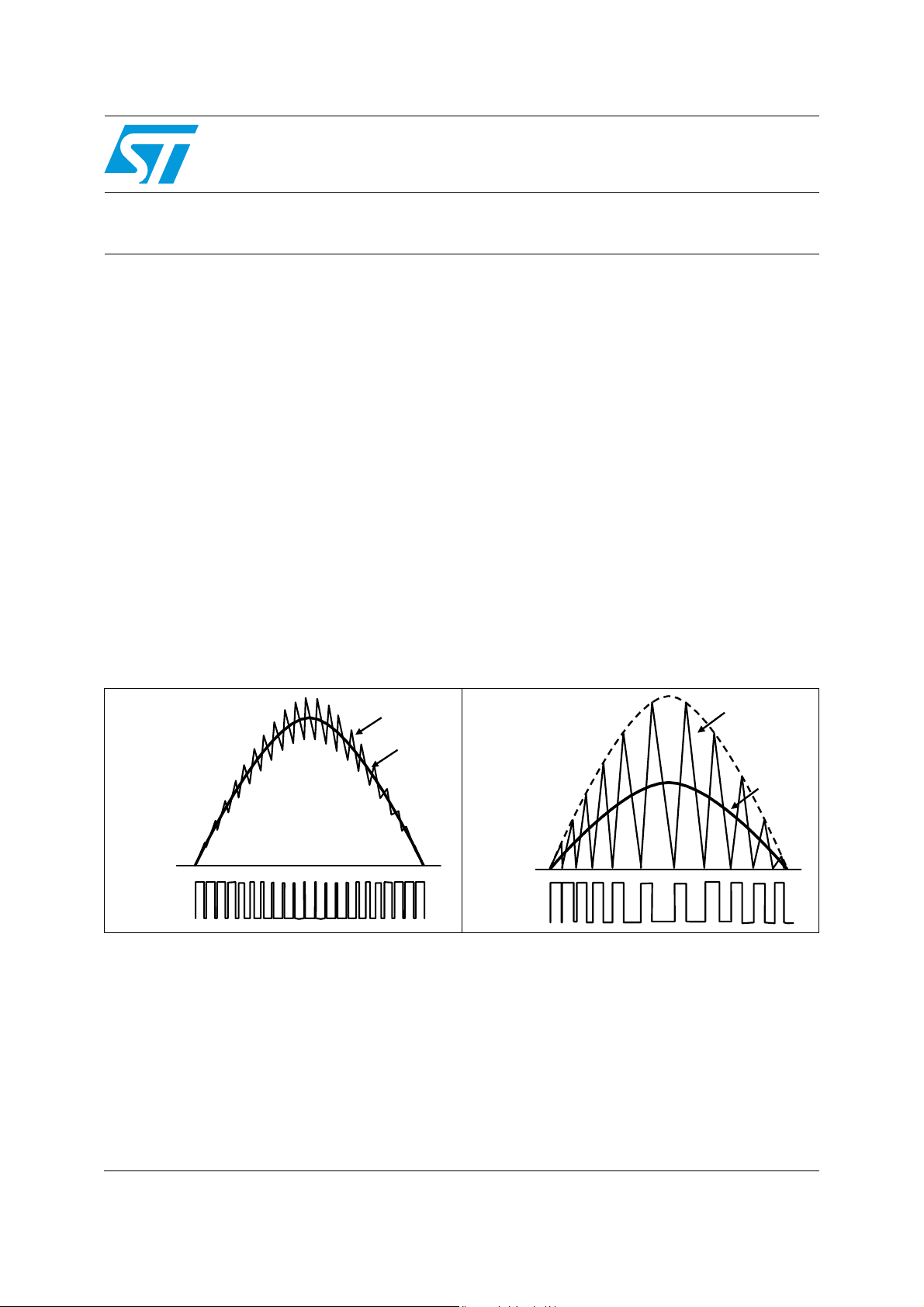
TM operation involves higher peak currents as compared to FF-CCM (Figure 1 and 2).
Figure 1. Line, inductor, switch and diode
currents in FF-CCM PFC
AN2782
Application note
Figure 2. Line, inductor, switch and diode
currents in TM PFC
"CCM" type
IL
"TM" type
IL
IAC
IAC
ON
MOSFET
OFF
This demonstration, consistent with the above mentioned cost considerations, suggests the
use of TM in a lower power range, while FF-CCM is recommended for higher power levels.
This criterion, though always true, is sometimes difficult to apply, especially for a midrange
power level, around 150-300 W. The assessment of which approach gives the better
cost/performance trade-off needs to be done on a case-by-case basis, considering the cost
and the stress of not only power semiconductors and magnetic but also of the EMI filter. At
the same power level, the switching frequency component to be filtered out in a TM system
is twice the line current, whereas it is typically 1/3 or 1/4 in a CCM system.
March 2010 Doc ID 14763 Rev 2 1/39
ON
MOSFET
OFF
www.st.com
Page 2

Contents AN2782
Contents
1 Introduction to FOT control . . . . . . . . . . . . . . . . . . . . . . . . . . . . . . . . . . . 4
2 Operation of an FOT-controlled PFC pre-regulator . . . . . . . . . . . . . . . . 5
3 The circuit implementing the line-modulated fixed off-time with the new
L6562A . . . . . . . . . . . . . . . . . . . . . . . . . . . . . . . . . . . . . . . . . . . . . . . . . . . . 6
4 Designing a fixed off-time PFC . . . . . . . . . . . . . . . . . . . . . . . . . . . . . . . . 9
4.1 Input specification . . . . . . . . . . . . . . . . . . . . . . . . . . . . . . . . . . . . . . . . . . . . 9
4.2 Operating condition . . . . . . . . . . . . . . . . . . . . . . . . . . . . . . . . . . . . . . . . . 11
4.3 Power section design . . . . . . . . . . . . . . . . . . . . . . . . . . . . . . . . . . . . . . . . 12
4.3.1 Bridge rectifier . . . . . . . . . . . . . . . . . . . . . . . . . . . . . . . . . . . . . . . . . . . . 12
4.3.2 Input capacitor . . . . . . . . . . . . . . . . . . . . . . . . . . . . . . . . . . . . . . . . . . . . 13
4.3.3 Output capacitor . . . . . . . . . . . . . . . . . . . . . . . . . . . . . . . . . . . . . . . . . . 13
4.3.4 Boost inductor . . . . . . . . . . . . . . . . . . . . . . . . . . . . . . . . . . . . . . . . . . . . 14
4.3.5 Power MOSFET selection and the dissipation . . . . . . . . . . . . . . . . . . . . 16
4.3.6 Boost diode selection . . . . . . . . . . . . . . . . . . . . . . . . . . . . . . . . . . . . . . . 18
4.3.7 L6562A biasing circuitry . . . . . . . . . . . . . . . . . . . . . . . . . . . . . . . . . . . . . 19
5 Design example using the L6562A FOT PFC Excel spreadsheet . . . . 28
6 EVL6562A-400W demonstration board . . . . . . . . . . . . . . . . . . . . . . . . . 30
7 Test results and significant waveforms . . . . . . . . . . . . . . . . . . . . . . . . 32
8 L6562A layout hints . . . . . . . . . . . . . . . . . . . . . . . . . . . . . . . . . . . . . . . . 36
9 Reference . . . . . . . . . . . . . . . . . . . . . . . . . . . . . . . . . . . . . . . . . . . . . . . . . 37
10 Revision history . . . . . . . . . . . . . . . . . . . . . . . . . . . . . . . . . . . . . . . . . . . 38
2/39 Doc ID 14763 Rev 2
Page 3

AN2782 List of figures
List of figures
Figure 1. Line, inductor, switch and diode currents in FF-CCM PFC. . . . . . . . . . . . . . . . . . . . . . . . . . 1
Figure 2. Line, inductor, switch and diode currents in TM PFC . . . . . . . . . . . . . . . . . . . . . . . . . . . . . . 1
Figure 3. Basic waveforms for fixed-frequency PWM . . . . . . . . . . . . . . . . . . . . . . . . . . . . . . . . . . . . . 4
Figure 4. Basic waveforms for fixed off-time PWM . . . . . . . . . . . . . . . . . . . . . . . . . . . . . . . . . . . . . . . 4
Figure 5. Block diagram of an FOT-controlled PFC pre-regulator . . . . . . . . . . . . . . . . . . . . . . . . . . . . 5
Figure 6. Circuit implementing FOT control with the L6562A. . . . . . . . . . . . . . . . . . . . . . . . . . . . . . . . 6
Figure 7. ZCD pin signal with the fixed off-time generator circuit. . . . . . . . . . . . . . . . . . . . . . . . . . . . . 7
Figure 8. Switching frequency fixing the line voltage . . . . . . . . . . . . . . . . . . . . . . . . . . . . . . . . . . . . . 15
Figure 9. The effect of fixing OFF-time - boundary between DCM and CCM . . . . . . . . . . . . . . . . . . 15
Figure 10. Conduction losses and total losses in the two STP12NM50 MOSFETs for the 400 W FOT
PFC . . . . . . . . . . . . . . . . . . . . . . . . . . . . . . . . . . . . . . . . . . . . . . . . . . . . . . . . . . . . . . . . . . . . . . 18
Figure 11. L6562A internal schematic . . . . . . . . . . . . . . . . . . . . . . . . . . . . . . . . . . . . . . . . . . . . . . . . . 19
Figure 12. Bode plot - open-loop transfer function. . . . . . . . . . . . . . . . . . . . . . . . . . . . . . . . . . . . . . . . 20
Figure 13. Bode plot - phase . . . . . . . . . . . . . . . . . . . . . . . . . . . . . . . . . . . . . . . . . . . . . . . . . . . . . . . . 20
Figure 14. Multiplier characteristics family . . . . . . . . . . . . . . . . . . . . . . . . . . . . . . . . . . . . . . . . . . . . . . 22
Figure 15. Switching frequency function on the peak of the sinusoid input voltage waveform and the cor-
responding off-time value . . . . . . . . . . . . . . . . . . . . . . . . . . . . . . . . . . . . . . . . . . . . . . . . . . . . . . . . . . . . 24
Figure 16. Off-time vs. input mains voltage . . . . . . . . . . . . . . . . . . . . . . . . . . . . . . . . . . . . . . . . . . . . . 26
Figure 17. Switching frequency vs. input mains voltage . . . . . . . . . . . . . . . . . . . . . . . . . . . . . . . . . . . 26
Figure 18. Excel spreadsheet design specification input table . . . . . . . . . . . . . . . . . . . . . . . . . . . . . . 28
Figure 19. Other design data . . . . . . . . . . . . . . . . . . . . . . . . . . . . . . . . . . . . . . . . . . . . . . . . . . . . . . . . 28
Figure 20. Excel spreadsheet FOT PFC schematic. . . . . . . . . . . . . . . . . . . . . . . . . . . . . . . . . . . . . . . 29
Figure 21. Excel spreadsheet BOM . . . . . . . . . . . . . . . . . . . . . . . . . . . . . . . . . . . . . . . . . . . . . . . . . . . 29
Figure 22. EVL6562A-400W demonstration board . . . . . . . . . . . . . . . . . . . . . . . . . . . . . . . . . . . . . . . 30
Figure 23. Wide-range 400 W demonstration board electrical circuit (EVL6562A-400W) . . . . . . . . . . 31
Figure 24. EVL6562A-400W compliance to EN61000-3-2 standard at full load . . . . . . . . . . . . . . . . . 32
Figure 25. EVL6562A-400W compliance to JEIDA-MITI standard at full load . . . . . . . . . . . . . . . . . . . 32
Figure 26. EVL6562A-400W compliance to EN61000-3-2 standard at 70 W . . . . . . . . . . . . . . . . . . . 32
Figure 27. EVL6562A-400W compliance to JEIDA-MITI standard at 70 W . . . . . . . . . . . . . . . . . . . . . 32
Figure 28. Power factor vs. Vin and load . . . . . . . . . . . . . . . . . . . . . . . . . . . . . . . . . . . . . . . . . . . . . . . 33
Figure 29. THD vs. Vin and load . . . . . . . . . . . . . . . . . . . . . . . . . . . . . . . . . . . . . . . . . . . . . . . . . . . . . 33
Figure 30. Efficiency vs. Vin and load . . . . . . . . . . . . . . . . . . . . . . . . . . . . . . . . . . . . . . . . . . . . . . . . . 33
Figure 31. Static Vout regulation vs. Vin and load . . . . . . . . . . . . . . . . . . . . . . . . . . . . . . . . . . . . . . . . 33
Figure 32. EVL6562A-400W: input current waveform at 100 V - 50 Hz - 400 W load . . . . . . . . . . . . . 34
Figure 33. EVL6562A-400W: input current waveform at 230 V -50 Hz - 400 W load . . . . . . . . . . . . . 34
Figure 34. EVL6562A-400W: input current waveform at 100 V - 50 Hz - 200 W load . . . . . . . . . . . . . 34
Figure 35. EVL6562A-400W: input current waveform at 230 V - 50 Hz - 200 W load . . . . . . . . . . . . . 34
Figure 36. EVL6562A-400W: input current waveform at 100 V - 50 Hz - 70 W load . . . . . . . . . . . . . . 35
Figure 37. EVL6562A-400W: input current waveform at 230 V - 50 Hz - 70 W load . . . . . . . . . . . . . . 35
Doc ID 14763 Rev 2 3/39
Page 4
Introduction to FOT control AN2782
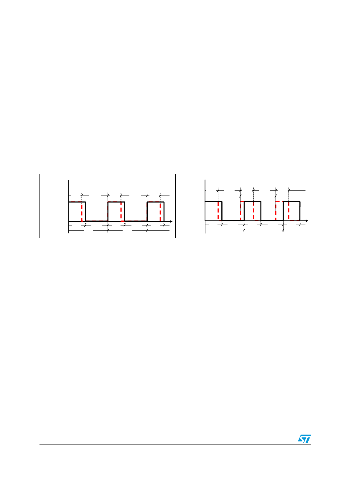
1 Introduction to FOT control
In this area where the TM/CCM usability boundary is uncertain, a third approach that
couples the simplicity and affordability of TM operation with the high-current capability of
CCM operation can be a solution to the dilemma. Generally speaking, FF PWM is not the
only alternative when CCM operation is desired. FF PWM modulates both switch ON and
OFF times (their sum is constant by definition), and a given converter operates in either
CCM or DCM depending on the input voltage and the loading conditions. Exactly the same
result can be achieved if the ON-time only is modulated and the OFF-time is kept constant,
in which case, however, the switching frequency is no longer fixed (Figure 3 and Figure 4).
This is referred to as “fixed off-time” (FOT) control. Peak-current-mode control can still be
used.
Figure 3. Basic waveforms for fixed-
Gate drive
signal
frequency PWM
TON'
TON'
TOFF'
TOFF'
TON
TON
TOFF
TOFF
TSW TSW
TSW TSW
TON'
TON'
TON
TON
TOFF'
TOFF'
TOFF
TOFF
TON'
TON'
TON
TON
An important point is that FOT control does not need a specialized control IC. A simple
modification of a standard TM PFC controller operation, requiring just a few additional
passive parts and no significant extra cost, is all that is needed.
Figure 4. Basic waveforms for fixed off-time
PWM
Gate drive
signal
TON' TON' TON'
TON' TON' TON'
TOFF TOFF
TOFF TOFF
TSW' TSW'
TSW' TSW'
TON TON TON TOFF TOFF
TON TON TON TOFF TOFF
TSW TSW
TSW TSW
4/39 Doc ID 14763 Rev 2
Page 5
AN2782 Operation of an FOT-controlled PFC pre-regulator
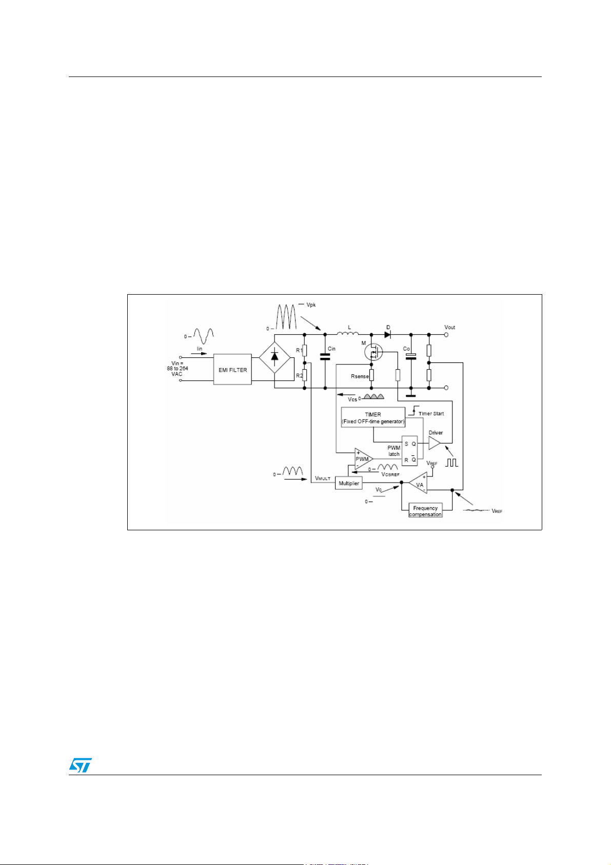
2 Operation of an FOT-controlled PFC pre-regulator
Figure 5 shows a block diagram of an FOT-controlled PFC pre-regulator. An error amplifier
(VA) compares a portion of the pre-regulator's output voltage Vout with a reference VREF
and generates an error signal V
hypothesis, is fed into an input of the multiplier block and multiplied by a portion of the
rectified input voltage V
V
, whose amplitude is proportional to that of V
CSREF
MULT
sinusoidal reference for PWM modulation. V
comparator that, on the non-inverting input, receives the voltage V
Rsense, proportional to the current flowing through the switch M (typically a MOSFET) and
the inductor L during the ON-time of M. When the two voltages are equal, the comparator
resets the PWM latch and M, supposedly already ON, is switched off.
Figure 5. Block diagram of an FOT-controlled PFC pre-regulator
proportional to their difference. VC, a DC voltage by
C
. At the output of the multiplier, there will be a rectified sinusoid,
and to VC, which represents the
MULT
is fed into the inverting input of a
CSREF
on the sense resistor
CS
As a result, V
determines the peak current through M and the inductor L. As V
CSREF
CSREF
is
a rectified sinusoid, the inductor peak current is enveloped by a rectified sinusoid as well.
The line current Iin will be the average inductor current that is the low-frequency component
of the inductor current resulting from the low-pass filtering operated by the EMI filter.
The PWM latch output Q going high activates the timer that, after a predetermined time
T
has elapsed, sets the PWM latch, thus turning M on and starting another switching
OFF
cycle. If T
is such that the inductor current does not fall to zero, the system operates in
OFF
CCM. It is apparent that FOT control requires nearly the same architecture as TM control,
just the way the off-time of M is determined changes. It is not a difficult task to modify
externally the operation of the standard TM PFC controller so that the off-time of M is fixed.
As a controller we will refer to the L6562A [4], which is suitable for a few hundred watts
power applications because of its gate drive capability and its high noise immunity.
For a more detailed and complex description of the fixed off-time technique and in particular
the line modulated FOT, please refer to [7].
Doc ID 14763 Rev 2 5/39
Page 6
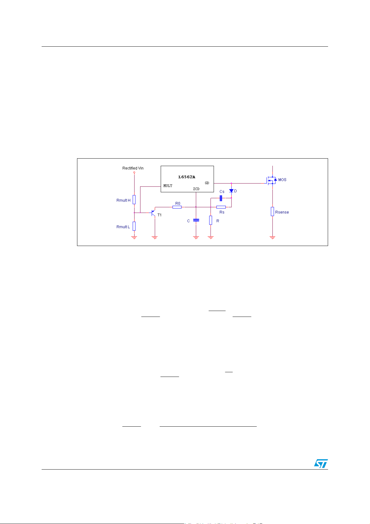
The circuit implementing the line-modulated fixed off-time with the new L6562A AN2782
(
3 The circuit implementing the line-modulated fixed
off-time with the new L6562A
The circuit that implements LM-FOT control with the L6562A is shown in Figure 6. During
the ON-time of the MOSFET the gate voltage V
biased and the voltage at the ZCD pin is internally clamped at V
off-time of M V
= 10 V is low, the diode D is reverse-biased and the voltage at the pin
GD
decays with an exponential law until it reaches the triggering threshold (V
that causes the switch to turn on. The time needed for the ZCD voltage to go from V
to V
ZCDtrigger
defines the duration of the off-time T
Figure 6. Circuit implementing FOT control with the L6562A
= 15 V is high, the diode D is forward-
GD
OFF
ZCDclamp
.
≈ 5.7 V. During the
ZCDtrigger
≈ 0.7 V)
ZCDclamp
The circuit of Figure 6 makes T
a function of the RMS line voltage thanks to the peak-
OFF
holding effect of T1 (which acts as a buffer) along with R and C whose time constant is
significantly longer than a line half-cycle. With the addition of R
voltage on the ZCD pin during T
is above V
OFF
mult+VBE
, C is discharged through R and R0,
and T, as long as the
0
following the law:
)RR(t
+⋅
0
−
′
As V’
⎡
V)t(V
⎢
ZCDclampZCD
⎣
(t) falls below V
ZCD
−=
0
mult+VBE
R
()
RR
+
, T1 is cut off and C is discharged through R only, so that
⎤
()
⋅
0
+⋅
eVV
⎥
BEmult
⎦
R
CRR
+⋅
()
RR
+
0
+⋅
(1)
VV
BEmult
its evolution from that point on is described by:
V'
(t) decreases from V
ZCD
′
t
′′
ZCD
ZCDclamp
⋅
RR
0
−=
+
RR
0
R
)t(V
=
()
RR
+
0
= 5.7 V to V
BEmult
mult+VBE
⎡
⋅⋅
lnC
⎢
⎢
⎣
t
−
CR
⋅
eVV
⋅+⋅
(2)
in the following time period t':
)
⋅+
RVV
0BEmult
()
⎤
⎥
⋅+−+⋅
RVV)RR(V
⎥
BEmult0ZCDclamp
⎦
(3)
6/39 Doc ID 14763 Rev 2
Page 7
AN2782 The circuit implementing the line-modulated fixed off-time with the new L6562A
and V''
(t) decreases from V
ZCD
mult+VBE
to V
ZCDtriggering
= 0.7 V level in the following time
period t'':
V
⎡
′′
⋅−=
lnRCt
ZCDtrigger
⎢
⎣
⎤
⎥
+
VV
BEmult
⎦
(4)
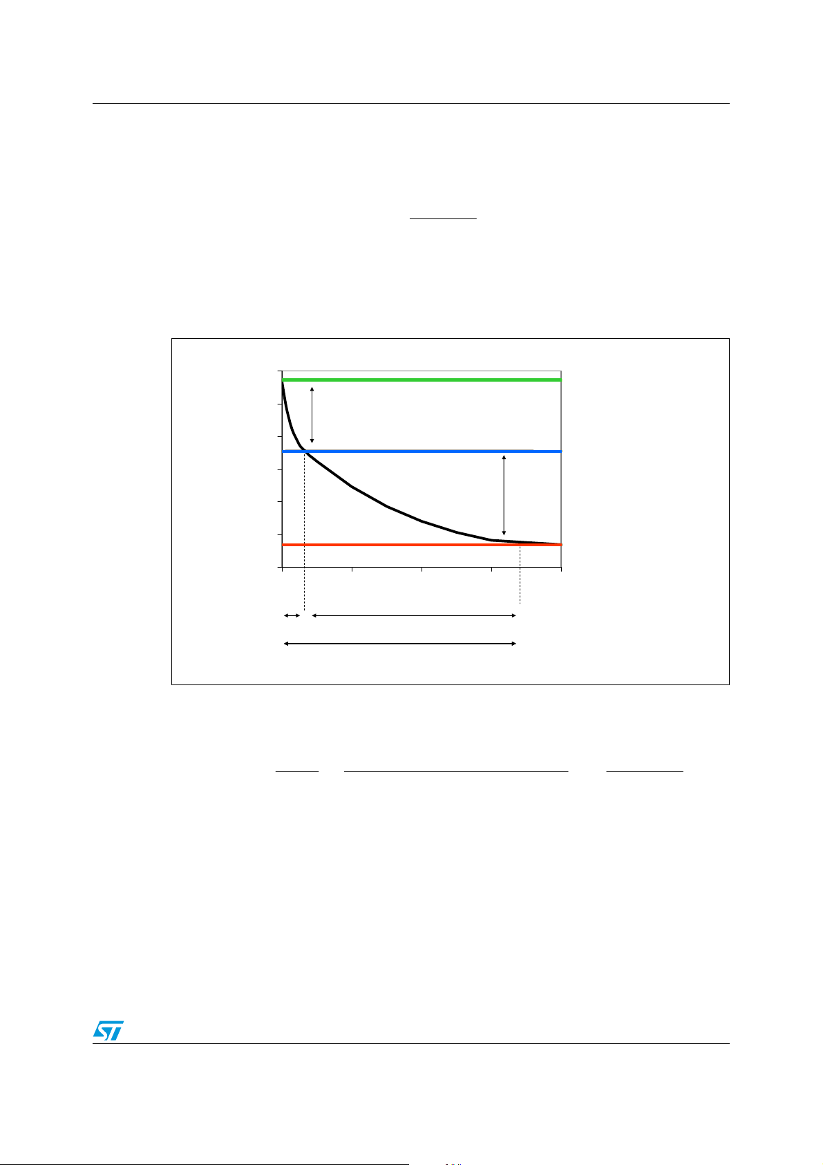
Figure 7 illustrates the signal on the ZCD pin with the two discharging time constants
depending on the two resistors R, R
and the L6562A parameters, particularly the upper
0
clamp voltage and the triggering voltage of the ZCD pin.
Figure 7. ZCD pin signal with the fixed off-time generator circuit
6
6
6
ZCDclamp
ZCDclamp
ZCDclamp
5
5
5
4
4
4
3
3
3
Vzcd (V)
Vzcd (V)
Vzcd (V)
2
2
2
′
′
′
ZCD
ZCD
ZCD
)(tV
)(tV
)(tV
′′
′′
′′
)(tV
)(tV
)(tV
ZCD
ZCD
ZCD
VV
7.5=
VV
7.5=
VV
7.5=
VV +
VV +
VV +
BEmult
BEmult
BEmult
1
1
1
0
0
0
02468
02468
02468
′
′
′
t
t
t
usec
usec
usec
′′
′′
′′
t
t
t
T
T
T
OFF
OFF
OFF
ZCDtrigger
ZCDtrigger
ZCDtrigger
VV
7.0=
VV
7.0=
VV
7.0=
The sum of the two time periods is the OFF-time function:
⎤
⎞
(5)
⎟
⎥
⎟
VV
⎥
BEmult
⎠
⎦
OFF
⎡
R
⎢
⋅−=
RCT
+
⎢
⎣
⎡
0
⋅
ln
⎢
RR
⎢
0
⎣
()
⋅+
RVV
0BEmult
()
In this way, once the multiplier operating point (that is, the V
proper selection of R and R
maximum line voltage, it is always T
condition needed in order to avoid line distortion [
It is easy to see that T
OFF
it is possible to increase T
0
ON>TONmin
= 450 ns for the L6562A [4]. This is a
OFF
7].
is now a function of the instantaneous line voltage. We will refer to
this technique as “line-modulated fixed off-time” (LM-FOT) [
⎤
⎥
⋅+−+⋅
RVV)RR(V
⎥
BEmult0ZCDclamp
⎦
/VAC ratio) is fixed, with a
mult
V
⎛
ZCDtrigger
⎜
+
ln
⎜
()
⎝
+
with the line voltage so that, at
7].
This modification, though simple, introduces profound changes in the timing relationships,
with a positive influence on the energetic relationships. From the control point of view,
modulating T
is a feedforward term that modifies the gain but does not change its
OFF
Doc ID 14763 Rev 2 7/39
Page 8

The circuit implementing the line-modulated fixed off-time with the new L6562A AN2782
characteristics. Consequently, all of the properties of the standard FOT control are
maintained.
Due to the highly non-linear nature of the T
modulation introduced by T1 and R0, its
OFF
effects are discussed only qualitatively and the quantitative aspects are provided graphically
for a specific case in [
7].
As a practical rule, it is convenient to first select a capacitor and then to calculate the resistor
needed to achieve the desired T
As the gate voltage V
as possible up to V
goes high, the resistor Rs charges the timing capacitor C as quickly
GD
ZCDclamp
, without exceeding clamp rating (I
(see Section 4.3.7).
OFF
=10 mA). Then it must
ZCDx
fulfill the following inequalities:
VVV
FZCDclampGD
(6)
= 15 V its
GDx
I
ZCDx
where V
(assume VGD = 10 V) is the voltage delivered by the gate driver, V
GD
maximum value, and V
VVV −−
−−
FZCDclampGDx
V
ZCDclamp
+
R
the forward drop on D.
F
RRs
⋅<<
V
ZCDclamp
When working at high line/light load the on-time of the power switch becomes very short and
the resistor Rs alone is no longer able to charge C up to V
ZCDclamp
. The speed-up capacitor
Cs is then used in parallel to Rs. This capacitor causes an almost instantaneous charge of C
up to a level, after that Rs completes the charge up to V
ZCDclamp
. It is important that the
steep edge caused by Cs does not reach the clamp level, otherwise the internal clamp of the
L6562A undergoes uncontrolled current spikes (limited only by the dynamic resistance of
the 1N4148 and the ESR of Cs) that could overstress the IC. Cs must then be:
V
CCs−−<
ZCDclamp
VVV
FZCDclampGDx
(7)
8/39 Doc ID 14763 Rev 2
Page 9

AN2782 Designing a fixed off-time PFC
=
=
=
=
=
=
Δ
4 Designing a fixed off-time PFC
4.1 Input specification
The following is a possible design flowchart in reference to a fixed off-time mode PFC using
the L6562A. This first part is a detailed specification of the operating conditions of the circuit
that is needed for the following calculations in
input range mains PFC circuit has been considered. Some design criteria are also given.
Section 4.2. In this example a 400 W, wide
● Mains voltage range (Vac rms):
● Minimum mains frequency:
● Rated output power (W):
min
Vac90VAC
l
out
max
Hz47f
W400P
Vac265VAC
=
(8)
(9)
(10)
Because the PFC is a boost topology the regulated output voltage depends strongly on the
maximum AC input voltage. In fact, for correct boost operation the output voltage must
always be higher than the input and thus, because Vin max is V
VAC
max
2 374=⋅
pk
, the
output has been set at 400 Vdc as the typical value. If the input voltage is higher, as typical
in ballast applications, the output voltage must be set higher accordingly. As a rule of thumb
the output voltage must be set 6/7% higher than the maximum input voltage peak.
● Regulated DC output voltage (Vdc):
out
V400V
(11)
The target efficiency and PF are set here at minimum input voltage and maximum load.
They are used for the following operating condition calculation of the PFC. Of course at high
input voltage the efficiency is higher.
P
● Expected efficiency (%):
● Expected power factor:
out
P
in
%90
==η
99.0PF
(12)
(13)
Because of the narrow loop voltage bandwidth, the PFC output can face overvoltages at
startup or in case of load transients. To protect from excessive output voltage that can
overstress the output components and the load, the L6562A integrates an OVP. The
overvoltage protection sets the extra voltage overimposed to Vout:
● Maximum output overvoltage (Vdc):
Doc ID 14763 Rev 2 9/39
V40OVP
(14)
Page 10

Designing a fixed off-time PFC AN2782
=
Δ
=
The mains frequency generates a 2fL voltage ripple on the output voltage at full load. The
ripple amplitude determines the current flowing into the output capacitor and the ESR.
Additionally, a certain holdup capability in case of mains dips can be requested from the
PFC in which case the output capacitor must also be dimensioned, taking into account the
required minimum voltage value (Vout min) after the elapsed holdup time (t
● Maximum output low frequency ripple:
● Minimum output voltage after line drop (Vdc):
● Holdup capability (ms):
out
Hold
V10V
=
minout
=
).
Hold
(15)
V300V
ms20t
(16)
(17)
The PFC minimum switching frequency is the one of the main parameters used to
dimension the boost inductor. Here we consider the switching frequency at low mains on the
top of the sinusoid and at full load conditions. As a rule of thumb, it must be higher than the
audio bandwidth in order to avoid audible noise and additionally it must not interfere with the
L6562A minimum internal starter period, as given in the datasheet. On the other hand, if the
minimum frequency is set too high the circuit shows excessive losses at higher input voltage
and probably operates skipping switching cycles not only at light load. Typical minimum
frequency range is 55÷95 kHz for wide range operation.
● Minimum switching frequency (kHz):
Where f
= 1/(T+220 nsec) due to the ZCD - gate drive signal delay typical of the
swmin
kHz72f
=
minsw
(18)
L6562A.
The design will be done on the basis of a ripple factor (the ratio of the maximum current
ripple amplitude to the inductor peak current at minimum line voltage) k
● Ripple factor
=0.36.
r
34.0k
r
(19)
In order to properly select the power components of the PFC and dimension the heat sinks
in case they are needed, the maximum operating ambient temperature around the PFC
circuitry must be known. Please note that this is not the maximum external operating
temperature of the entire equipment, but it is the local temperature at which the PFC
components are working.
● Maximum ambient temperature (°C)
ambx
C50T
°=
(20)
10/39 Doc ID 14763 Rev 2
Page 11

AN2782 Designing a fixed off-time PFC
4.2 Operating condition
The first step is to define the main parameters of the circuit, using the specification points
given in
● Rated DC output current
● Maximum input power
Section 4.1:
P
out
out
I
out
V
out
P
in
W400
90
I =
P
out
=
P
in
η
W400
==
V400
=⋅=
(21)
A00.1
(22)
W44.444100
Referring to the main currents shown in
Figure 1, the following formula expresses the
maximum value of current circulating in the boost cell which means at minimum line voltage
of the selected range:
● RMS input current
P
I
=
in
out
min
I
=
in
PFVAC
⋅
W400
=
99.0Vac90
⋅
(23)
A99.4
It is important to define the following ratios in order to continue describing the energetic
relationships in the PFC:
VAC
min
min
max
2k =
2k =
V
VAC
V
out
max
out
min
max
Vac90
2k
Vac265
2k
32.0
==
V400
94.0
==
V400
(24)
(25)
From (24), (25):
P2
● Line peak current:
⋅
I
=
maxPK
in
I
Vk
⋅
outmin
maxPK
⋅
=
)W44.444(2
=
V400318.0
⋅
(26)
A98.6
● Inductor ripple-
ΔILpk:
IL ⋅
=Δ
pk
Doc ID 14763 Rev 2 11/39
k6
⋅
r
I
k38
⋅−
r
IL
maxPK
=Δ
pk
34.06
⋅
34.038
⋅−
=⋅
(27)
A18.2A98.6
Page 12

Designing a fixed off-time PFC AN2782
● Inductor peak
current:
IL ⋅
maxpk
8
=
I
k38
⋅−
r
IL
maxPK
maxpk
8
=
34.038
⋅−
=⋅
(28)
A07.8A98.6
It is also possible to calculate the RMS current flowing into the switch and into the diode,
needed to calculate the losses of these two elements.
● RMS
switch
current:
● RMS
diode
current:
ISW
ID
rms
rms
P
in
=
⋅
Vk
outmin
P
in
=
⋅
Vk
outmin
It is worth reminding that the accuracy of the approximate energetic relationships described
here is quite good at maximum load for low values of the parameter k, that is, at low line
voltage, but worsens at high line and as the power throughput is reduced. Since in the
design phase current stress is calculated at maximum load and minimum line voltage, their
accuracy is acceptable for design purposes.
4.3 Power section design
4.3.1 Bridge rectifier
The input rectifier bridge can use standard slow recovery, low-cost devices.Typically a
600 V device is selected in order to have good margin against mains surges. An NTC
resistor limiting the current at turn-on is required to avoid overstress to the diode bridge.
⋅
k16
min
ISW
rms
rms
=
=
−⋅
2
π
3
k16
min
⋅
3
ID
π
W400
⋅
W400
⋅
2
V400318.0
⋅
V400318.0
318.016
⋅
−⋅
⋅
3
=
3
π
318.016
=
π
A22.4
A57.2
(29)
(30)
The rectifier bridge power dissipation can be calculated using equations
threshold voltage and dynamic resistance of a single diode of the bridge can be found in the
component datasheet.
I2
⋅
I
=
inrms
I
avg_in
in
2
I2
⋅
=
in
π
⋅
=
2
⋅
=
The power dissipated on the bridge is:
12/39 Doc ID 14763 Rev 2
(31), (32), (33). The
A99.42
=
A99.42
π
A53.3
=
A25.2
(31)
(32)
Page 13

AN2782 Designing a fixed off-time PFC
bridge
2
diodebridge
inrms
2
IV4IR4P ⋅⋅+⋅⋅=
avg_inth
W53.7A25.2V7.04)A53.3(025.04P
=⋅⋅+⋅Ω⋅=
(33)
4.3.2 Input capacitor
The input filter capacitor, Cin, is placed across the diode bridge output. This capacitor must
smooth the high-frequency ripple and must sustain the maximum instantaneous input
voltage. In a typical application an EMI filter is placed between the mains and the PFC
circuit. In this application the EMI filter is reinforced by a differential mode Pi-filter after the
bridge to reject the differential noise coming from the whole switching circuit.
The design of the EMI filter (common mode and differential mode) is not described here.
The value of the input filter capacitor can be calculated as follows, simply considering the
output power that the PFC should deliver at full load:
in
The maximum value of this capacitor is limited to avoid line current distortion. The value
chosen for this demonstration board is 1 µF.
4.3.3 Output capacitor
The output bulk capacitor (Co) selection depends on the DC output voltage (11), the allowed
overvoltage
The 100/120 Hz (twice the mains frequency) voltage ripple (ΔVout = (Vout = peak-to-peak
ripple value)
With a low ESR capacitor the capacitive reactance is dominant, therefore:
(14), and the converter output power (10).
(15) is a function of the capacitor impedance and the peak capacitor current:
I
C
≥
O
out
Δ⋅⋅π
Vf2
3
ESR
−
2
W400
⋅⋅⋅π
F1W400105.2C
μ=⋅⋅=
F338
V10V400Hz472
μ=
(34)
(35)
(36)
−
3
P105.2C ⋅⋅=
out
I2V +
⋅⋅=Δ
outout
P
=
outl
out
Δ⋅⋅⋅π
VVf2
outoutl
in
1
2
)Cf22(
⋅⋅π
Ol
C
≥
O
ΔVout is usually selected in the range of 1.5% of the output voltage.
Although ESR usually does not affect the output ripple, it should be taken into account for
power loss calculations. The total RMS capacitor ripple current, including mains frequency
and switching frequency components, is:
Crms
2
rms
2
IIDI −=
out
Crms
()()
Doc ID 14763 Rev 2 13/39
22
=−=
(37)
A36.2A0.1A56.2I
Page 14

Designing a fixed off-time PFC AN2782
(
()(
[
]
If the PFC stage has to guarantee a specified holdup time, the selection criterion of the
capacitance changes. Co has to deliver the output power for a certain time (t
Hold
) with a
specified maximum dropout voltage (Vout min) that is the minimum output voltage value
(which takes load regulation and output ripple into account). Vout min is the minimum output
operating voltage before the 'power fail' detection and consequent stopping by the
downstream system supplied by the PFC.
⋅⋅
tP2
out
Holdout
2
2
−Δ−
VVV
C
=
O
minout
()()
=
C
O
()
out
ms20W4002
⋅⋅
22
V300V10V400
−−
F3.242
μ=
(38)
A 20% tolerance on the electrolytic capacitors has to be taken into account for the right
dimensioning.
Following the relationship
selected in order to maintain a holdup capability for 20 ms. The actual output voltage ripple
with this capacitor is also calculated. In detail:
As expected, the ripple variation on the output is:
V
=Δ
out
4.3.4 Boost inductor
In the continuous mode approach, the acceptable current ripple factor, Kr, can be
considered between 10% to 35%. For this design, the maximum specified current ripple
factor is 35%.
t
Hold
(38), for this application a capacitor Co = 330 µF (450 V) has been
⎡
O
out
⎢
t
Hold
=
I
out
Cf2
⋅⋅π⋅
Ol
⎣
=
⋅
2
)
−Δ−⋅
out
P2
⋅
out
−−⋅μ
W4002
V
=Δ
out
⎤
2
VVVC
minout
⎥
⎦
22
)
V300V10V400F330
ms22
=
A0.1
F330Hz472
μ⋅⋅π⋅
V2.10
=
(39)
(40)
To calculate the required inductance L of the boost inductor, use the following formula with a
4.2 µs OFF-time set at 90Vac (see the following ZCD pin dimensioning for finding the correct
value):
V
min
out
)k1()VAC(L
⋅−=
Δ
IL
OFF
pk
)VAC(T
min
)32.01()VAC(L
After calculating the values of the inductor at low mains and at high mains L(VAC
L(VAC
) (41) depending also on the OFF-time, the minimum value has to be taken into
min
V400
A11.2
max
(41)
H520s2.4
μ=μ⋅−=
),
account. It became the maximum inductance value for the PFC dimensioning.
14/39 Doc ID 14763 Rev 2
Page 15

AN2782 Designing a fixed off-time PFC
θ
θ
1
θ2
Figure 8 shows the switching frequency versus the θ angle calculated inverting the (41), with
a 500 µH boost inductance and fixing the line voltage at minimum and maximum values.
Figure 8. Switching frequency fixing the line voltage
Frequency modulation with the Line half period
1000
CCM
DCM
100
kHz
DCM
10
1
TM
Switching Freq.@VacMin
Switching Freq.@VacMax
0 0.4 0.8 1.2 1.6 2 2.4 2.8
[
Line half period]
TM
Figure 9. The effect of fixing OFF-time - boundary between DCM and CCM
CCM
CCM
TM
TM
DCM
DCM
Half Line Cycle
TOFF
TOFF
θ1
θ1
Half Line Cycle
The effect of fixing the OFF-time is generating a continuous conduction mode in the center
region of the line half-cycle between the two transition angles. Close to the zero-crossing,
the system works in discontinuous conduction mode and in transition mode at the boundary.
The core size is determined assuming a peak flux density Bx ≅
0.25 T (depending on the
ferrite grade selected and relevant specific losses) and calculating the maximum current
according to
(28) as a function of the maximum current sense pin clamping voltage and
sense resistor value.
DC and AC copper losses and ferrite losses must also be calculated to determine the
maximum temperature rise of the inductor.
Doc ID 14763 Rev 2 15/39
Page 16

Designing a fixed off-time PFC AN2782
(
4.3.5 Power MOSFET selection and the dissipation
The selection of the MOSFET concerns mainly its R
(10), since the breakdown voltage is fixed just by the output voltage (11), plus the
power
overvoltage allowed
(15) and a safety margin (20%).
, which depends on the output
DS(on)
Thus, a voltage rating of 500 V (1.2 · Vout = 480 V) is selected. Using its current rating as a
rule of thumb, we can select a device having ~ 3 times the RMS switch current
(29) but, the
power dissipation calculation gives the final confirmation that the selected device is the right
one for the circuit also taking into account the heat sink dimensions. In this 400 W TM PFC
application two parallel STP12NM50 MOSFETs have been selected in order to support the
high inductor current.
The MOSFET's power dissipation depends on conduction, switching and capacitive losses.
The conduction losses at maximum load and minimum input voltage are calculated by:
Because normally in the datasheets the R
2
)
rms)on(DScond
is given at ambient temperature (25 °C) to
DS(on)
)VAC(ISWR)VAC(P ⋅=
(42)
calculate correctly the conduction losses at 100°C (typical MOSFET junction operating
temperature), a factor of 1.75 to 2 should be taken into account. The exact factor can be
found in the device datasheet.
Now, the conduction losses referred to as 1 Ω R
and VAC can be calculated, combining equations (42) and (29):
of P
in
at ambient temperature as a function
DS(on)
⎛
′
rmscond
2
⋅=⋅=
2))VAC(ISW(2)VAC(P
P
⎜
⎜
⎝
in
⋅
V)VAC(k
out
The switching losses due to the MOSFET current-voltage I
MOS
2
−⋅
, V
⋅
3
crossing occurs at
MOS
2
⎞
)VAC(k16
⎟
⎟
π
⎠
(43)
turn-on and turnoff because of the FOT operation and can be basically expressed by:
tt
+
⎛
IV)VAC(P
⋅⋅=
⎜
MOSMOSswitch
⎝
⎞
fallrise
⋅
⎟
2
sw
⎠
)VAC(f
(44)
Because the switching frequency depends on the input line voltage and on the position on
the sinusoidal waveform, it can be demonstrated that from
(44) the switching losses per 1 µs
of current rise and fall time can be written as:
⎛
′
⎜
ILV)VAC(P
maxpkoutswitch
⎜
⎝
From the selected MOSFET datasheet t
−⋅=
rise
Δ
IL
2
= t
π
⎞
1
pk
⎟
⋅
⎟
∫
π
⎠
0
= 0.01 µs is the crossover time at turn-on
fall
2
()
sw
ϑ⋅θ⋅ϑ
d),VAC(fsin
(45)
and off.
At turn-on the losses are due to the discharge of the total drain capacitance inside the
MOSFET itself.
16/39 Doc ID 14763 Rev 2
Page 17

AN2782 Designing a fixed off-time PFC
In general, the capacitive losses are given by:
1
)VAC(P
2
2
⋅⋅⋅=
MOS
dcap
sw
)VAC(fVC
(46)
where C
capacitances such as inductor etc. At the drain node, V
is the total drain capacitance including the MOSFET and the other parasitic
d
is the drain voltage at MOSFET
MOS
turn-on.
Taking into account the frequency variation with the input line voltage and the phase angle
similar to
(45), a detailed description of the capacitive losses per 1 nF of total drain
capacitance can be calculated as:
′
)VAC(P
The total drain capacitance of the two MOSFETs is //Cd = 0.36 nF, V
π
121
()
⋅=
outcap
∫
π
0
2
sw
ϑ⋅ϑ
d),VAC(fV
is the drain voltage
out
(47)
at MOSFET turn-on.
The function of the total losses of the input mains voltage is the sum of the three previous
losses from equations
(43), (45) and (47) multiplied for the two parallel MOSFET
parameters:
+
tt
′
⋅=
condonloss
From
(48) using the data relevant to the MOSFET selected and calculating the losses at
⎛
+
)VAC(PRDS)VAC(P
⎜
⎝
⎞
fallrise
′
⋅
⎟
2
⎠
′
⋅+
capdsw
)VAC(PC)VAC(P
(48)
VACmin and VACmax, we observe that the maximum total losses occurs at VACmin which is
9 W. From this number and the maximum ambient temperature
(20), the total maximum
thermal resistance required to keep the junction temperature below 125 °C is:
TC125
R
=
th
If the result of equation
loss
−°
ambx
)VAC(P
=
R
th
°−°
C50C125
W9
(49) is lower than the junction-ambient thermal resistance given in
°
C
=
1.8
W
the MOSFET datasheet for the selected device package, a heat sink must be used.
Doc ID 14763 Rev 2 17/39
(49)
Page 18

Designing a fixed off-time PFC AN2782
(
Figure 10. Conduction losses and total losses in the two STP12NM50 MOSFETs for
the 400 W FOT PFC
15
10
Dissipation (W)
5
0
90 115 140 165 190 215 240 265
Figure 10
shows the trend of the total losses (48) on the line voltage for the two selected
STP12NM50 MOSFETs.
4.3.6 Boost diode selection
Following a similar criterion as that for the MOSFET, the output rectifier can also be
selected. A minimum breakdown voltage of 1.2·(Vout + ΔOVP) and a current rating higher
than 3·Iout
is then confirmed by the thermal calculation. If the diode junction temperature works within
125 °C the device has been selected correctly, otherwise a bigger device must be selected.
(21) can be chosen for a rough initial selection of the rectifier. The correct choice
MOSFETS total losses
Pcond(Vi)
Plosse s(Vi)
Vac (V)
The switching losses can be significantly reduced if an ultra-fast diode is employed. Since
this circuit operates in the continuous current mode, the MOSFET has to recover the boost
diode minority carrier charge at turn-on. Thus, a diode with a small reverse recovery time,
trr, must be used.
In this 400 W application an STTH8R06, (600 V, 8 A) has been selected. The STTH8R06
offers the best solution for the continuous current mode operation due to its very fast reverse
recovery time, 25 ns typical. This part has a breakdown voltage rating (Vrrm) of 600 V,
average forward current rating (Ifave) of 8 A and reverse recovery time (trr) of 25 ns.
The rectifier AVG
threshold voltage) and R
(21) and RMS (30) current values and the parameter V
(dynamic resistance) given in the datasheet allow calculating the
d
rectifier losses.
From the STTH8R06 datasheet, V
2
IDRIVP ⋅+⋅=
rms
doutthdiode
18/39 Doc ID 14763 Rev 2
is 1.16 V, Rd is 0.08 Ω, neglecting the recovery losses:
th
diode
(rectifier
th
2
)
=⋅Ω+⋅=
(50)
W69.1A56.208.0A0.1V16.1P
Page 19

AN2782 Designing a fixed off-time PFC
V
From (20) and (50) the maximum thermal resistance to keep the junction temperature below
125 °C is then:
TC125R−°
P
ambx
diode
=
th
=
R
th
°−°
C50C125
=
W68.1
°
C
45.44
W
(51)
The diode is attached to the same heat sink as the power MOSFET. The STTH8R06 has an
isolated package and can be attached directly to the heat sink. Silicone thermal grease may
be applied to improve the thermal contact between the diode and heat sink.
4.3.7 L6562A biasing circuitry
Following the dimensioning of the power components, the biasing circuitry for the L6562A is
also described. For reference, the internal schematic of the L6562A is represented below in
Figure 11. For more details on the internal functions, please refer to the datasheet.
Figure 11. L6562A internal schematic
INV COMP MULT CS
123 4
ERROR
INTERNAL
SUPPLY BUS
UVLO
V
REF2
AMPLIFIER
VREF
-
+
1.4 V
0.7 V
5
= 2.5V
ZCD
-
+
OVERVOLTAGE
DETECTION
DYN
OVP
DIS
ZERO CURRENT
+
-
STAT
OVP
DETECTOR
MUL TIP LI ER AN D
THD OPTIMIZER
1 V
+-
COMP ARATO R
R
Q
S
PWM
STARTER
Starte r
stop
outH
LEADI NG-ED GE
BLANKING
and R
VCC
DRIVER
& CLAMP
outL
7
6
are then selected
GD
GND
DIS
-
0.45 V
+
0.2 V
VOLTAGE
REGULATOR
8
CC
25 V
LOWER & UPPER
CLAMPS
● Pin 1 (INV): This pin is connected both to the inverting input of the E/A and to the OVP
circuitry. A resistive divider is connected between the boost regulated output voltage
and this pin. The internal reference on the non-inverting input of the E/A is 2.5 V (typ),
while the OVP intervention threshold is 27 µA (typ). R
as follows:
R
outH
R
outL
R
outH
V
out
V5.2
V
Δ
OVP
=
A27
μ
R
outH
1
−= 1591
R
outL
= M481.1
R
outH
V400
V5.2
V40
μ
A27
=−=
Ω=
(52)
(53)
Doc ID 14763 Rev 2 19/39
Page 20

Designing a fixed off-time PFC AN2782
μ
=Ω=
R
outL
159
R
R
outH
= Ω== k32.9
outL
R
159
outH
(54)
The commercial values selected are R
Please note that for R
a resistor with a suitable voltage rating (>400 V) is needed, or
outH
outH
more resistors in series have to be used.
This pin can also be used as an ON/OFF control input if tied to GND by an open collector or
open drain.
● Pin 2 (COMP): This pin is the output of the E/A that is fed in one of the two inputs of the
multiplier. A feedback compensation network is placed between this pin and INV [
has to be designed in with a narrow bandwidth in order to avoid that the system rejects
the output voltage ripple (100 Hz) that would bring high distortion of the input current
waveform. A theoretical criterion to define the compensation network value is to set the
E/A bandwidth (BW) from 20 to 30 Hz.
For a more complex way of compensating the FOT PFC please refer to [
A compensated two-pole feedback network for this 400 W FOT PFC has been obtained with
the following values:
nF220C
= F2.2C
compP
compS
to which correspond the following open-loop transfer function and its phase function.
Figure 12. Bode plot - open-loop transfer
100
function
Open Loop Transfer Function
IFI
= 1530 MΩ and R
compS
= 9.5 kΩ.
outL
k47R
Figure 13. Bode plot - phase
Phase F
-100
1]. It
1], [2], [3].
(55)
0
dB
-100
-200
0.1 1 10 100 1000
f [Hz]
deg
-150
-200
0.1 1 10 100 1000
The two bode plot charts are in reference to the PFC operating at the main voltage set point
of 265 Vac and full load. In this condition the crossover frequency is fc = 25 Hz, the phase
margin is 30 ° and the third harmonic distortion is under 3%.
● Pin 4 (CS): Pin #4 is the inverting input of the current sense comparator. Through this
pin, the L6562A reads the instantaneous inductor current, converted to a proportional
20/39 Doc ID 14763 Rev 2
f [Hz]
Page 21

AN2782 Designing a fixed off-time PFC
(
⋅−⋅
=
voltage by an external sense resistor (Rs). As this signal crosses the threshold set by
the multiplier output, the PWM latch is reset and the power MOSFET is turned off. The
MOSFET stays in OFF-state until the PWM latch is reset by the ZCD signal. The pin is
equipped with 200 ns leading-edge blanking for improved noise immunity.
The sense resistor value (R
) can be calculated as follows. For the 400 W PFC it is:
s
R <
sx
Vcs
IL
maxpk
min
R
sx
V0.1
A07.8
Ω=< 124.0
(56)
where:
● IL
● Vcs
is the maximum peak current in the inductor, calculated as described in (28)
pkmax
= 1.0 V is the minimum voltage allowed on the L6562A current sense (in the
min
datasheet)
Because the internal current sense clamping sets the maximum current that can flow in the
inductor, the maximum peak of the inductor current is calculated considering the maximum
voltage Vcs
The calculated IL
allowed on the L6562A (in the datasheet):
max
Vcs
max
IL
IL =
pksat
is the limit at which the boost inductor saturates and it is used for
pksat
R
s
pksat
=
V16.1
=
12.0
Ω
A67.9
(57)
calculating the inductor number of turns and air gap length.
The power dissipated in R
is given by:
s
2
ISWRP ⋅=
rmsss
s
It does not exceed 1% of the rated output power
(10), that is, 4 W.
2
)
=⋅Ω=
W14.2A54.1012.0P
(58)
According to the result, four parallel resistors of 0.47 Ω with 1 W of power rating have been
selected.
● Pin 3 (MULT): The MULT pin is the second multiplier input. It is connected, through a
resistive divider, to the rectified mains to get a sinusoidal voltage reference. The
multiplier can be described by the relationship:
V)V5.2V(kV
MULTCOMPCS
(59)
where:
● V
● k = 0.38 (typ) is the multiplier gain
● V
● V
(multiplier output) is the reference for the current sense
CS
is the voltage on pin 2 (E/A output)
COMP
is the voltage on pin 3
MULT
Doc ID 14763 Rev 2 21/39
Page 22

Designing a fixed off-time PFC AN2782
Figure 14. Multiplier characteristics family
Multiplier characteristic
1.2
Uppe r Volt. Clamp
1.1
1.0
0.9
0.8
0.7
0.6
0.5
Vcs (pin4) (V)
0.4
0.3
0.2
0.1
0.0
-0.1
0.00.2 0.40.60.81.01.21.41.61.82.02.22.42.62.83.0
5.75 V
5 V
4.5V
VMULT (pin3) (V)
V COMP (pin2) (V
4 V
)
3.5V
3 V
2.5 V
A complete description is given in Figure 14, which shows the typical multiplier
characteristics family. The linear operation of the multiplier is guaranteed within the range 0
to 3 V of V
and the range 0 to 1.16 V (typ) of VCS, while the minimum guaranteed value
MULT
of the maximum slope of the characteristics family (typ) is:
dV
dV
CS
MULT
V
=
1.1
V
(60)
Taking this into account, the following is the suggested procedure to properly set the
operating point of the multiplier.
First, the maximum peak value for V
MULT
, VMULT
is selected. This value, which occurs at
max
maximum mains voltage, should be 3 V or nearly so in wide range mains and less in case of
single mains. The sense resistor selected is R
= 0.117 Ω and it is described in the
s
paragraph concerning pin 4 of this section. The maximum peak value, occurring at
maximum mains voltage, is:
RIL
⋅
VAC
where IL
VMULT ⋅
VMULT
and Rs have been already calculated, and 1.1 V/V is the multiplier maximum
pksat
max
=
max
=
1.1
spksat
1.1
117.0A67.9
Ω⋅
VAC
Vac265
Vac90
max
min
(61)
=⋅
V02.3
slope, as given in the datasheet.
22/39 Doc ID 14763 Rev 2
Page 23

AN2782 Designing a fixed off-time PFC
From (60) the maximum required divider ratio is calculated as:
V
k
=
p
maxMULT
VAC2
⋅
=
max
V02.3
Vac2652
⋅
3
−
1008.8
⋅=
(62)
Supposing a 300 µA current flowing into the multiplier divider the lower resistor value can be
calculated:
V
= k03.10
R
multL
maxMULT
μ
A300
=
V02.3
μ
A300
Ω=
(63)
A commercial value of 10 kΩ for the lower resistor is selected. The upper resistor value can
now be calculated:
−
=
R
multH
k
In this application example R
Please note that for R
a resistor with a suitable voltage rating (> 400 V) is needed, or
multH
k1
p
p
multH
=
R
multL
= 1240 MΩ and a R
3
−
⋅−
1008.81
−
3
⋅
1008.8
= 10 kΩ have been selected.
multL
Ω=Ω
M238.1k10
(64)
more resistors in series must be used.
The voltage on the multiplier pin with the selected component values re-calculated is 1.01 V
at minimum line voltage and is 2.99 V at maximum line voltage. The multiplier works
correctly within its linear region.
● Pin 5 (ZCD) is the input to the zero current detector circuit. It is connected to the line-
modulated, fixed off-time circuit seen in the previous
Figure 6 on page 6. Referring to
Section 3: The circuit implementing the line-modulated fixed off-time with the new
L6562A
pair of the desired values for T
(T
, the starting point for the design of the zero-current detector (ZCD) circuit is the
on the top of the line voltage sinusoid at minimum
OFF
OFF
at VAC
) obtained by setting the switching
max
OFF
at VAC
) and maximum line (T
min
frequency on the peak of the sinusoid at low mains and considering the minimum ontime of the L6562A:
k
min
)VAC(T =
minOFF
f
minsw
minOFF
32.0
)VAC(T
kHz72
s2.4ns220
μ=−=
(65)
)VAC(T
=
where f
VAC
min
maxOFF
is the switching frequency on the top of the sinusoid of the input voltage at
swmin
= 90 Vac (Figure 15).
k1
−
Let ρx as the ratio between
kT
⋅
max
maxminON
)VAC(T
=
maxOFF
94.0ns450
⋅
94.01
−
s8.6ns220
μ=−
(66), (65):
Doc ID 14763 Rev 2 23/39
(66)
Page 24

Designing a fixed off-time PFC AN2782
)VAC(T
=ρ 63.1
x
maxOFF
)VAC(T
minOFF
=ρ
x
s8.6
μ
=
s2.4
μ
(67)
In the formula (65), (66) the delay between the ZCD signal and the gate drive signal is taken
into account in order to increase the accuracy of the mathematical model.
From the theory of the line-modulation fixed off-time, T
so that at maximum line voltage, the condition T
L6562A [
4]. This is important in order to avoid line distortion [7].
ON>TONmin
is increasing with the line voltage
OFF
= 450 ns is always true for the
Figure 15. Switching frequency function on the peak of the sinusoid input voltage
waveform and the corresponding off-time value
TOFF@VACmax
TOFF@VACmax
TOFF@VACmax
6
6
6
5
5
5
4
4
4
3
3
3
Vzcd (V)
Vzcd (V)
Vzcd (V)
2
2
2
1
1
1
0
0
0
02468
02468
02468
TOFF@VACmin
TOFF@VACmin
TOFF@VACmin
6
6
5
5
4
4
3
3
Vzcd (V)
Vzcd (V)
2
2
1
1
0
0
012345
012345
usec
usec
Vin [Vac]
Vin [Vac]
Vin [Vac]
fswmax
fswmax
fswmax
usec
usec
usec
fswmin
fswmin
fswmin
Input Line Voltage
Input Line Voltage
Input Line Voltage
90Vac
90Vac
90Vac
Switching
Switching
Switching
Frequency
Frequency
Frequency
Function
Function
Function
0
0
0
p
p
p
265Vac
265Vac
265Vac
Angle
Angle
Angle
Now considering the two discharging resistors R and R0 of the circuit of Figure 6, the ratio
is defined:
K
1
R
=
1
+
0
τ
where 0 < K
time constant τ =(R//R
< 1.Through the definition of the parameter K2 it is underlined the expected
1
)C necessary to achieve the desired T
0
Finding a way to obtain K
K
=
K
2
and K2 means increasing the values of R and R0 and the
1
discharging time constant of the capacitor C.
The following part describes the mathematical way to obtain the two parameters K
Combining
(65), (66), (68) and (69) with the expression of the off-time (5) the following
expressions are obtained:
24/39 Doc ID 14763 Rev 2
RR
(68)
at 90 Vac.
OFF
)VAC(T
minOFF
(69)
and K2.
1
Page 25

AN2782 Designing a fixed off-time PFC
=ρ−
ρ
=
=
=
−
k1
⎡
⎡
⎢
⎢
⎢
ln
⎢
⎢
⎢
⎣
=ρ
)k,V(
1minmult
1minmult2
⎡
⎢
V
⎢
⎢
⎣
⎢
⎡
⎢
⎢
⎢
⎢
⎣
⎣
⎡
⎢
⎢
⎣
⎡
1
−
⎢
)k,V(k
=
⎢
k1
−
⎣
VAC
minmult
⎡
ln
⎢
[]
⎢
⎣
ln
⋅
1
max
VAC
min
⎡
VV
⎢
minmultZCDclamp
⎣
[]
⎡
[]
⎢
⎢
⎣
⎤
max
min
−⋅
⎥
⎦
)k1(V
1F
⎤
⎤
+⋅−
⋅
⎥
⎥
⎥
⎦
⎦
−⋅+
)k1(VV
1Fminmult
⋅+−
+⋅
VAC
VAC
[]
−⋅+
[]
1
⎤
⎥
⎥
⎥
⎥
)k(V
1F
⎥
⎦
⎤
⎥
)k(VVV
⎥
1FminmultZCDclamp
⎦
)k1(VV
1Fminmult
⎛
⎜
V
V
V
ZCDtrigger
ln
+
minmult
+
⎛
⎜
⎜
⎝
ZCDtrigger
VAC
VAC
⎤
⎞
⎥
⎟
⎟
⎥
VV
Fminmult
⎠
⎦
V
ZCDtrigger
max
min
⎜
+
ln
⎜
⎜
⎝
−
k1
1
⎛
⎜
+
ln
⎜
⎝
k1
−
1
⎤
⎥
kVVV
⋅+−
⎥
1FminmultZCDclamp
⎦
⎤
⎞
⎥
⎟
⎥
⎟
⎥
⎟
⎥
+⋅
V
⎟
F
(70)
⎥
⎠
⎥
⎦
⎤
⎞
(71)
⎥
⎟
⎟
⎥
VV
+
Fminmult
⎠
⎦
From (70) and (71), solving the following equation:
0)k,V(
x1minmult
91.0K
1
(72)
And then substituting the value of K
into the expression in (70), the K2 parameter is
1
obtained:
From the values of K
and K2 it is possible to calculate the time constant τ =(R1//R2) C
1
necessary to achieve the desired T
=τ
K
2
at 90Vac:
OFF
)VAC(T
minOFF
)k,V(kK
1minmult22
=τ
46.12
46.12K
2
s2.4=μ
ns7.336
Now selecting a capacitor C in the hundred pF or few nF, for example C =120 pF, it is
possible to determine the required equivalent resistance value:
ns7.336
pF120
Ω== k81.2
From
(67) R and R
R
eq
are found:
0
τ
=
R
C
eq
(73)
(74)
(75)
R−=
R
eq
K1
1
= k5.31
R
Ω
k81.2
−
94.01
Ω=
(76)
Doc ID 14763 Rev 2 25/39
Page 26

Designing a fixed off-time PFC AN2782
Ω<<
Ω
R =
0
R
eq
K
1
= k08.3
R
0
Ω
k81.2
94.0
Ω=
(77)
Commercial values R = 30 kΩ and a R0 = 3 kΩ have been chosen.
Figure 16 and Figure 17 show the trend of the OFF-time and the switching frequency vs. the
input mains voltage. The PFC inner current loop is working in the range 72 kHz - 132 kHz.
Due to the tolerance of the capacitor selected C and the two discharging resistors, it is
important to take into account a variation on the switching frequency in a real board of about
+- 10%.
Figure 16. Off-time vs. input mains voltage Figure 17. Switching frequency vs. input
10
8
160
140
120
mains voltage
6
TOFF [us]
4
2
0
90 115 140 165 190 215 240 265
Finally the limiting resistor R
Vin_ac [Vrms]
should be selected according to the inequalities (6).
s
−−
mA10
+
k81.2
and the speed-up capacitor C
s
100
80
fs [kHz]
60
40
20
0
90 115 140 165 190 215 240 265
V6.0V7.5V15 −−
V7.5
k81.2Rs
Ω
using (7):
pF120Cs
⋅<
Vin_ac [Vrms]
⋅Ω<<
V7.5
V7.5
V6.0V7.5V15
−−
V6.0V7.5V10
(78)
(79)
that means after algebra:
k94.1Rs790
26/39 Doc ID 14763 Rev 2
(80)
Page 27

AN2782 Designing a fixed off-time PFC
<
pF6.78Cs
(81)
A commercial value of the limiting resistor of 1.8 kΩ and a speed-up capacitor of 68 pF has
been selected for this application.
● Pin 6 (GND): This pin acts as the current return both for the signal internal circuitry and
for the gate drive current. When laying out the printed circuit board, these two paths
should run separately.
● Pin 7 (GD) is the output of the driver. The pin is able to drive an external MOSFET with
600 mA source and 800 mA sink capability. The high-level voltage of this pin is clamped
at about 12 V to avoid excessive gate voltages in case the pin is supplied with a high
Vcc. To avoid undesired switch-on of the external MOSFET because of some leakage
current when the supply of the L6562A is below the UVLO threshold, an internal pulldown circuit holds the pin low. The circuit guarantees 1.1 V maximum on the pin (at
Isink = 2 mA), with Vcc > VCC_ON. This allows omitting the “bleeder” resistor
connected between the gate and the source of the external MOSFET used for this
purpose.
● Pin 8 (Vcc) is the supply of the device. This pin is externally connected to the startup
circuit (usually, one resistor connected to the rectified mains) and to the self-supply
circuit. Whatever the configuration of the self-supply system, a capacitor is connected
between this pin and ground. To start the L6562A, the voltage must exceed the startup
threshold (12.5 V typ). Below this value the device does not work and consumes less
than 30 µA (typ) from Vcc. This allows the use of high value startup resistors (in the
hundreds kΩ), which reduces power consumption and optimizes system efficiency at
low load, especially in wide-range mains applications. When operating, the current
consumption (of the device only, not considering the gate drive current) rises to a value
depending on the operating conditions but never exceeding 3.75 mA. The device keeps
on working as long as the supply voltage is over the UVLO threshold (10.5 V max). If
the Vcc voltage exceeds 25 V an internal Zener diode, 20 mA rated, is activated in
order to clamp the voltage. Please remember that during normal operation the internal
Zener does not have to clamp the voltage, in which case the power consumption of the
device increases considerably and its junction temperature also increases. The
suggested operating condition for safe operation of the device is below the minimum
clamping voltage of the pin.
Doc ID 14763 Rev 2 27/39
Page 28

Design example using the L6562A FOT PFC Excel spreadsheet AN2782
5 Design example using the L6562A FOT PFC Excel
spreadsheet
An Excel spreadsheet has been developed to allow a quick and easy design of a boost PFC
pre-regulator using the STM L6562A controller, operating in fixed off-time.
Figure 18 shows the first sheet already precompiled with the input design data used in the
previous
Figure 18. Excel spreadsheet design specification input table
Section 4: Designing a fixed off-time PFC.
Parameter Name Value Unit [ ]
Mains Voltage Range VacMin 90 VACrms
Mains Voltage Range VacMax 265 VACrms
Min.Mains Frequency fl 47 Hz
Regulated Output Voltage Vout 400 Vdc
Rated Output Power Pout 400 W
Max. Output Low Frequency Ripple ǻ Vout 10 Vpk-pk
Max. Output Overvoltage ǻOVP 40 Vdc
Holdup Capability Thold 20 ms
Min. Output Voltage after Line drop VoutMin 300 Vdc
Min. Switching Frequency: fmin 72 kHz
Expected Efficiency
Expected Power Factor PF 0.99 ---
Max ind.curr.ripple to peak ratio VACmin,Pout_max) Kr 0.34 ---
Maximum Ambient Temperature Tambx 50 C
η
90 %
Figure 19. Other design data
Parameter Name Value Unit [ ]
Maximum Magnetic Flux Density Bx 0.25 T
Ripple VoltageCoefficient r 0.1 ---
The tool is able to generate a complete part list of the PFC schematic represented in
Figure 20, including the power dissipation calculation of the main components.
28/39 Doc ID 14763 Rev 2
Page 29

AN2782 Design example using the L6562A FOT PFC Excel spreadsheet
Figure 20. Excel spreadsheet FOT PFC schematic
Vac (88V - 264V)
Bridge
Cin
L
1 2
CcompS
VCC
Rmult HRmult L
VCC
MULT
T
Rzc d3
Rcom pS
Ccom pP
COMP INV
2
8
L6562A
3
5
6
ZCD
Rzc d2
Czc d2
Rzc d1
Czcd1
1
GD
7
4
CSGND
D
+
RoutH
Cout
MOS
RoutL
Rsens e
-
0
The bill of material in Figure 21 is automatically compiled by the Excel spreadsheet. It
summarizes all selected components and some salient data.
Figure 21. Excel spreadsheet BOM
400 W FOT PFC BASED ON L6562A
BILL OF MATERIAL
Selected
Value
BRIDGE RECTIFIER D15XB60
MOSFET P/N 2 x STP12NM50FP
DIODE P/N STTH8R06
Inductor Lx 500
Max peak Inductor current Ilpkx 9.67 A
Sense resistor Rsx 0.12 ȍ
Power dissipation Ps 2.14 W
INPUT Capacitor Cin 1
OUTPUT Capacitor Cout 330
MULT Divider Rmult L 10 kȍ
ZCD set Rzcd1 30 kȍ
Diode P/N 1N4148
pnp-BJT P/N BC857C
Feedback Divider RoutH 1530 kȍ
Comp Network CcompP 220 nF
IC Controller L6562A
Rmult H 1240 kȍ
Rzcd2 1.8 kȍ
Rzcd3 3 kȍ
Czcd1 120 pF
Czcd2 68 pF
RoutL 9.5 kȍ
CcompS 2200 nF
RcompS 47 kȍ
Unit [ ]
H
F
F
The following section is dedicated to report the main bench evaluation results of the 400 W
FOT PFC with the L6562A available for the customer as an demonstration board.
Doc ID 14763 Rev 2 29/39
Page 30

EVL6562A-400W demonstration board AN2782
6 EVL6562A-400W demonstration board
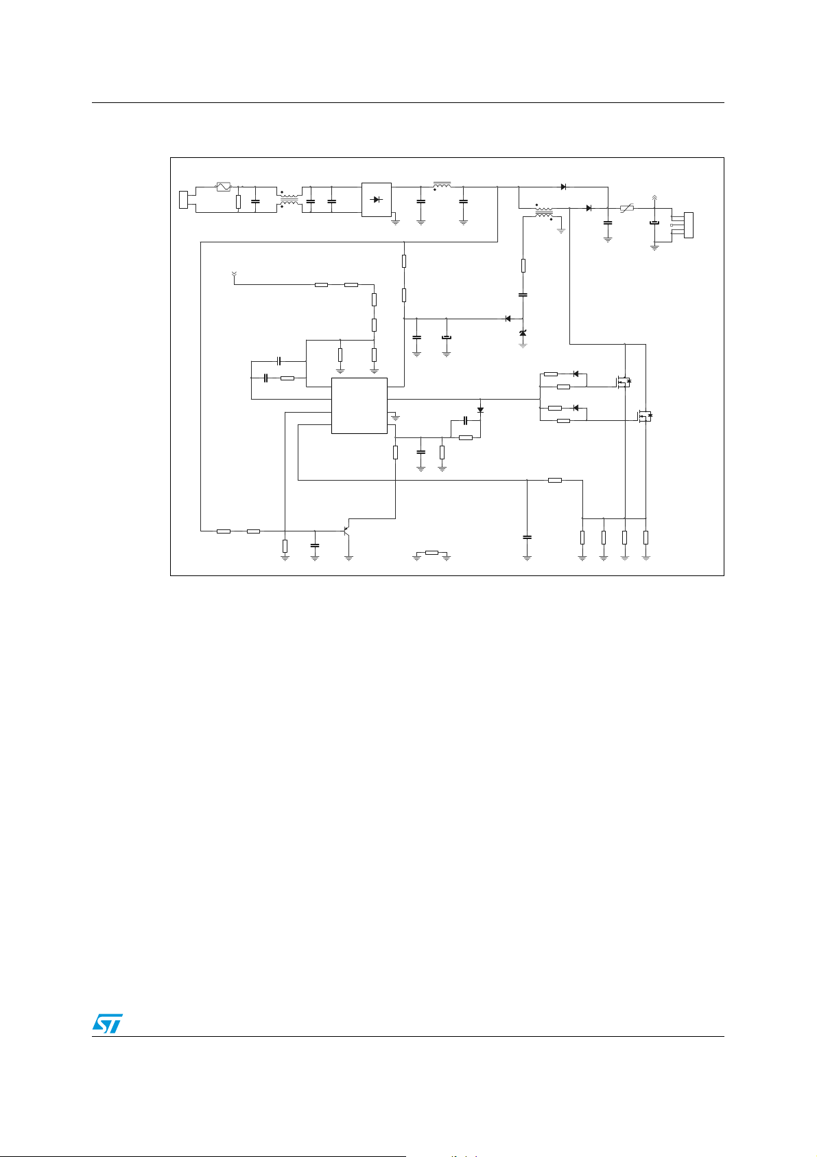
Figure 23 shows the schematic of an application board. It has been dimensioned using the
Excel tool presented in
The board implements a power factor correction (PFC) pre-regulator delivering 400 W,
continuous power, on a regulated 400 V rail from a wide-range mains voltage and providing
for the reduction of the mains harmonics, which complies with the European norm
EN61000-3-2 or the Japanese norm JEIDA-MITI. This rail is the input for the cascaded
isolated DC-DC converter that provides the output rails required by the load.
The board has been designed to allow full-load operation in still air.
Figure 22. EVL6562A-400W demonstration board
Section 5.
30/39 Doc ID 14763 Rev 2
Page 31
AN2782 EVL6562A-400W demonstration board
Figure 23. Wide-range 400 W demonstration board electrical circuit (EVL6562A-
400W)
L3
DM-51uH-6A
C4
470nF-630V
R3
100K
R4
100K
C11
470nF/50V
8
7
6
5
R31
3k
C16
120pF
R16
30k
C12
100uF/50V
C15
68pF
C5
470nF-630V
R15
1k8
811
D4
LL4148
LL4148
D6
5-6
T
PQ40-500uH
R5
47R
C10
22N
D5
BZX85-C18
D1
1N5406
1-2
D3
STTH8R06
C6
470nF-630V
R2
NTC 2R5-S237
330uF-450V
+400Vdc
J2
1
+400Vdc
2
+400Vdc
3
NC
C7
4
RTN
5
RTN
+400Vout
D7
LL4148
D8
LL4148
STP12NM50FP
Q1
Q2
STP12NM50FP
R36
3R9
R17
6R8
R35
3R9
R18
6R8
R19
1K0
J1
1
2
90 - 265Vac
8A/250V
D2
C3
680nF-X2
INV
COMP
MULT
R10
510k
R12
47K
L6562A
D15XB60
~
+
-
~
R102
0R0
R11
510k
R13
12k
VCC
GD
GND
ZCDCS
+400Vdc
CM-1.5mH -5A
L1
C1
R1
470nF-X2
1M5
C14
2.2uF
C2
470nF
R9
510k
C13
220nF
R14
47k
1
2
3
4
F1
R33
R32
620k
620k
R34
10k
Q3
BC857C
C21
10nF
R101
0R0
C20
330pF
R20
0R47-1W
R21
0R47-1W
R22
0R47-1W
R23
0R47-1W
The power stage of the PFC is a conventional boost converter, connected to the output of
the rectifier bridge D2. It includes the coil T, the diode D3 and the capacitors C6 and C7. The
boost switch is represented by the power MOSFETs Q1 and Q2. The NTC R2 limits the
inrush current at switch-on. It has been connected on the DC rail, in series to the output
electrolytic capacitor, in order to improve the efficiency during low-line operation.
Additionally, the splitting in two of output capacitors (C6 and C7) provides for managing the
AC current mainly by the film capacitor C6 so that the electrolytic can be cheaper as it has
just to bear the DC part.
At startup the L6562A is powered by the Vcc capacitor (C12) that is charged via the
resistors R3 and R4, then the T secondary winding (pins 8-11) and the charge pump circuit
(R5, C10, D5 and D4) generates the Vcc voltage powering the L6562A during the normal
operations.
The divider R32, R33 and R34 provides the L6562A multiplier with the information of the
instantaneous voltage that is used to modulate the boost current. The divider R9, R10, R11,
R12 & 13 is dedicated to sense the output. The line-modulated FOT is obtained by the
timing generator components D6, C15, R15, C16, R16, R31, Q3.
The board is equipped with an input EMI filter designed for a 2-wire input mains plug. It is
composed of two stages, a common mode Pi-filter connected at the input (C1, L1, C2, C3)
and a differential mode Pi-filter after the input bridge (C4, L3, C5). It also offers the
possibility to easily connect a downstream converter.
Doc ID 14763 Rev 2 31/39
Page 32

Test results and significant waveforms AN2782
7 Test results and significant waveforms
One of the main purposes of a PFC preconditioner is the correction of input current
distortion, decreasing the harmonic contents below the limits of the relevant regulations.
Therefore, this demonstration board has been tested according to the European standard
EN61000-3-2 Class-D and Japanese standard JEIDA-MITI Class-D, at full load at both
nominal input voltage mains.
As reported in the following
Figure 24, Figure 25, Figure 26 and Figure 27 the circuit is able
to reduce the harmonics well below the limits of both regulations from full load down to light
load. Please note that all measures and waveforms have been done using a common mode
Pi-filter connected at the input (C1, L1, C2, C3) and a differential mode Pi-filter after the
input bridge for filtering the noise coming from the circuit.
Figure 24. EVL6562A-400W compliance to
Harmo nic c urren t (A)
0.001
0.0001
EN61000-3-2 standard at full load
Mea surem ents @ 230Vac Fu ll loa d EN61000-3-2 class D limits
10
1
0.1
0.01
1 3 5 7 9 11131517 19212325272931 33353739
Harmonic Order (n)
Figure 26. EVL6562A-400W compliance to
EN61000-3-2 standard at 70 W
Measurements @ 230Vac 70W EN61000-3-2 cla ss D limi ts
1
Figure 25. EVL6562A-400W compliance to
JEIDA-MITI standard at full load
Measurements @ 100Vac Full load JEIDA-MITI class D limits
10
1
0.1
0.01
Harmonic current (A)
0.001
0.0001
1 3 5 7 9 11 13 15 17 19 21 23 25 27 29 3 1 33 35 37 39
Harmonic Order (n)
Figure 27. EVL6562A-400W compliance to
JEIDA-MITI standard at 70 W
Measurements @ 100Vac 70W JEIDA-M ITI cla ss D lim its
1
0.1
0.01
Harmonic current (A)
0.001
0.0001
1 3 5 7 9 1113 15 1719 2123 252729313335 3739
Harmonic Order (n)
0.1
0.01
Harmo nic curren t (A)
0.001
0.0001
32/39 Doc ID 14763 Rev 2
1 3 5 7 9 111315171921232527293133353739
Harmonic Order (n)
Page 33
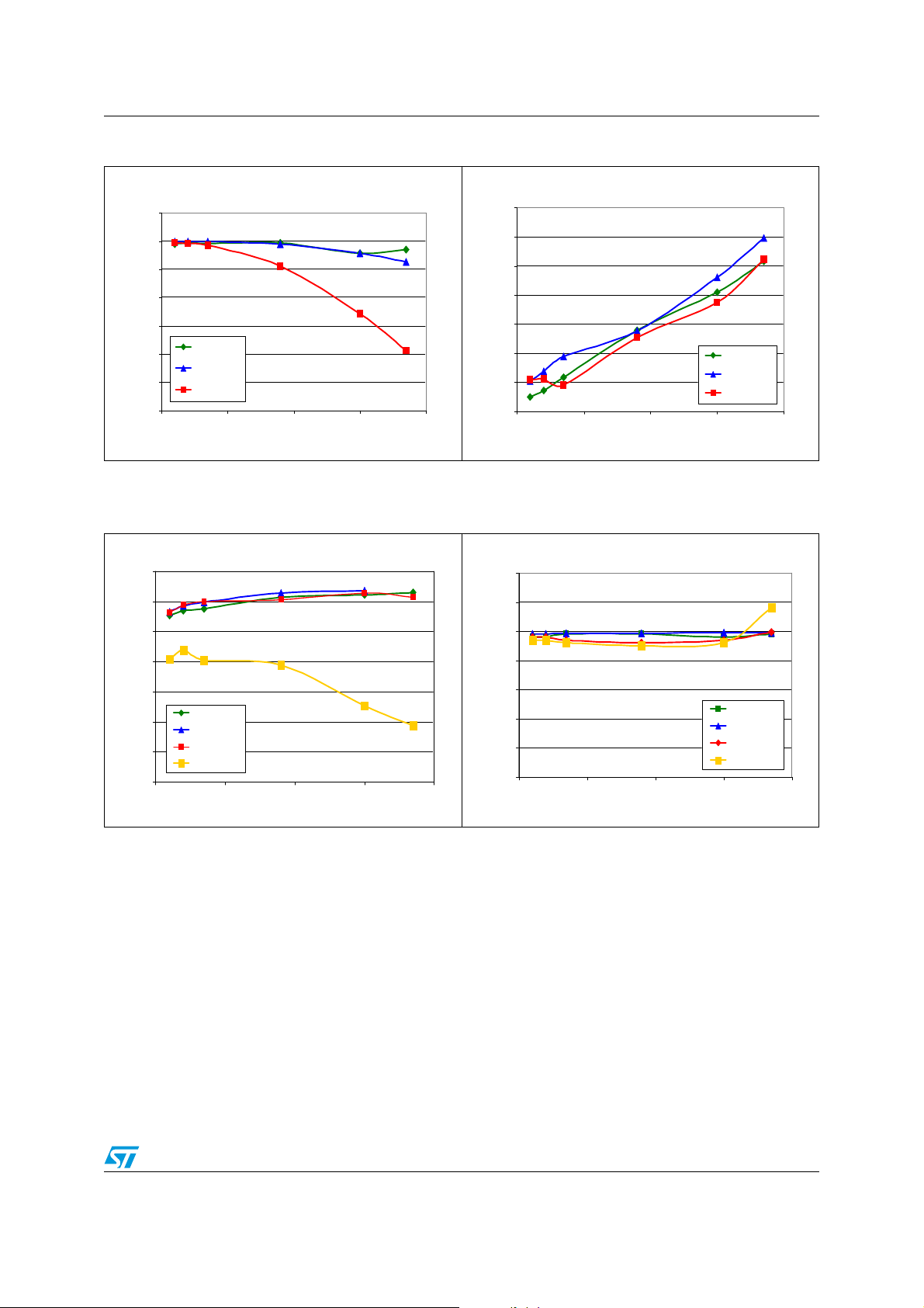
AN2782 Test results and significant waveforms
Figure 28. Power factor vs. Vin and load Figure 29. THD vs. Vin and load
1.05
1.00
0.95
0.90
PF
0.85
0.80
0.75
0.70
Pout = 400W
Pout = 200W
Pout = 70W
80 130 180 230 280
Vin (Vac)
35
30
25
20
15
THD (%)
10
5
0
80 130 180 230 280
Vin (Vac)
Pout = 400W
Pout = 200W
Pout = 70W
Figure 30. Efficiency vs. Vin and load Figure 31. Static Vout regulation vs. Vin and
100
404
load
95
90
85
ξ
80
75
70
65
Pout = 400W
Pout = 200W
Pout = 70 W
Pout = 15W
80 130 180 230 280
Vin (Vac)
The power factor (PF) and the total harmonic distortion (THD) have been measured too and
the results are illustrated in
Figure 28, 29, 30, 31. As shown, the PF at full load and half load
remains close to unity throughout the input voltage mains range while, when the circuit is
delivering 70 W, it decreases at high mains range. THD is low, remaining within 30% at
maximum input voltage.
The efficiency is very good at all load and line conditions. At full load it is always significantly
higher than 90%, making this design suitable for high-efficiency power supplies.
The measured output voltage variation at different line and load conditions is shown in
Figure 28, 29, 30, 31. As shown, the voltage is perfectly stable over the entire input voltage
range. Just at 265Vac and light load, there are negligible deviations of 1 V due to the
intervention of the burst mode (for the “static OVP”) function.
403
402
401
400
Vout (Vdc)
399
398
397
80 130 180 230 280
Vin (Vac)
Pout = 400W
Pout = 200W
Pout = 70W
Pout = 15W
Doc ID 14763 Rev 2 33/39
Page 34

Test results and significant waveforms AN2782
For user reference, waveforms of the input current and voltage at the nominal input voltage
mains and different load conditions are shown in
Figure 32 through Figure 37.
Figure 32. EVL6562A-400W: input current
waveform at 100 V - 50 Hz - 400 W
load
Figure 34. EVL6562A-400W: input current
waveform at 100 V - 50 Hz - 200 W
load
Figure 33. EVL6562A-400W: input current
waveform at 230 V -50 Hz - 400 W
load
Figure 35. EVL6562A-400W: input current
waveform at 230 V - 50 Hz - 200 W
load
34/39 Doc ID 14763 Rev 2
Page 35

AN2782 Test results and significant waveforms
Figure 36. EVL6562A-400W: input current
waveform at 100 V - 50 Hz - 70 W
load
Figure 37. EVL6562A-400W: input current
waveform at 230 V - 50 Hz - 70 W
load
Doc ID 14763 Rev 2 35/39
Page 36

L6562A layout hints AN2782
8 L6562A layout hints
The layout of any converter is a very important phase in the design process that sometimes
does not get enough attention from the engineers. Even if it the layout phase sometimes
looks time-consuming, a good layout does indeed save time during the functional debugging
and the qualification phases. Additionally, a power supply circuit with a correct layout needs
smaller EMI filters or less filter stages which allows consistent cost savings.
The L6562A does not need any special attention to the layout, simply the general layout
rules for any power converter must be carefully applied. Basic rules are listed below which
can be used for other PFC circuits having any power level, working either in TM or with an
FOT-control mode.
1. Keep power and signal RTN separated. Connect the return pins of components
carrying high current such as input capacitors, sense resistors, or output capacitors as
close as possible. This point is the RTN star point. A downstream converter or ballast
must be connected to this return point.
2. Minimize the length of the traces relevant to the boost inductor, boost rectifier and
output capacitor.
3. Keep signal components as close as possible to the L6562A pins. Specifically, keep the
tracks relevant to pin #1 (INV) net as short as possible. Components and traces
relevant to the error amplifier have to be placed far from traces and connections
carrying signals with high dv/dt like the MOSFET drain.
4. Connect heat sinks to power GND.
5. Place an external copper shield around the boost inductor and connect it to power
GND.
6. Please connect the RTN of signal components including the feedback and MULT
dividers close to the L6562A pin #6 (GND).
7. Connect a ceramic capacitor (100÷470 nF) to pin #8 (Vcc) and to pin #6 (GND), close
to the L6562A. Connect this point to the RTN star point 1.
36/39 Doc ID 14763 Rev 2
Page 37

AN2782 Reference
9 Reference
1. “A New Continuous-Time Model for Current-Mode Control with Constant Frequency,
Constant On-Time and Constant Off-Time, in CCM and DCM”, IEEE Power Electronics
Specialists Conference Record, San Antonio, Texas, pp. 382-389, 1990
2. “Current Mode Control”, Venable Technical Paper #5, www.venableind.com
3. “Fixed off-time Control of PFC pre-regulators”, 10th European Conference on Power
Electronics and Applications, EPE2003, Toulouse, France, paper 382
4. “L6562A, Transition-Mode PFC Controller”, datasheet, www.st.com
5. “Filter Inductor and Flyback Transformer Design for Switching Power Supplies”,
UNITRODE Power Supply Design Seminar Manual, 1994 (SEM-1000)
6. “L6561, Enhanced Transition Mode Power Factor Corrector”, AN966, www.st.com
7. “Design fixed off-time controlled PFC pre-regulators with the L6562”, AN1792
8. “400W FOT-controlled PFC pre-regulator with the L6563”, AN2485
9. “A systematic Approach to Frequency Compensation of the Voltage loop in boost PFC
pre-regulator”, Abstract
10. “Control loop modelling of L6561-based TM PFC”, AN1089
Doc ID 14763 Rev 2 37/39
Page 38

Revision history AN2782
10 Revision history
Table 1. Document revision history
Date Revision Changes
20-Aug-2008 1 Initial release
05-Mar-2010 2 Updated Coverpage, Section 3 and equation (28)
38/39 Doc ID 14763 Rev 2
Page 39

AN2782
Please Read Carefully:
Information in this document is provided solely in connection with ST products. STMicroelectronics NV and its subsidiaries (“ST”) reserve the
right to make changes, corrections, modifications or improvements, to this document, and the products and services described herein at any
time, without notice.
All ST products are sold pursuant to ST’s terms and conditions of sale.
Purchasers are solely responsible for the choice, selection and use of the ST products and services described herein, and ST assumes no
liability whatsoever relating to the choice, selection or use of the ST products and services described herein.
No license, express or implied, by estoppel or otherwise, to any intellectual property rights is granted under this document. If any part of this
document refers to any third party products or services it shall not be deemed a license grant by ST for the use of such third party products
or services, or any intellectual property contained therein or considered as a warranty covering the use in any manner whatsoever of such
third party products or services or any intellectual property contained therein.
UNLESS OTHERWISE SET FORTH IN ST’S TERMS AND CONDITIONS OF SALE ST DISCLAIMS ANY EXPRESS OR IMPLIED
WARRANTY WITH RESPECT TO THE USE AND/OR SALE OF ST PRODUCTS INCLUDING WITHOUT LIMITATION IMPLIED
WARRANTIES OF MERCHANTABILITY, FITNESS FOR A PARTICULAR PURPOSE (AND THEIR EQUIVALENTS UNDER THE LAWS
OF ANY JURISDICTION), OR INFRINGEMENT OF ANY PATENT, COPYRIGHT OR OTHER INTELLECTUAL PROPERTY RIGHT.
UNLESS EXPRESSLY APPROVED IN WRITING BY AN AUTHORIZED ST REPRESENTATIVE, ST PRODUCTS ARE NOT
RECOMMENDED, AUTHORIZED OR WARRANTED FOR USE IN MILITARY, AIR CRAFT, SPACE, LIFE SAVING, OR LIFE SUSTAINING
APPLICATIONS, NOR IN PRODUCTS OR SYSTEMS WHERE FAILURE OR MALFUNCTION MAY RESULT IN PERSONAL INJURY,
DEATH, OR SEVERE PROPERTY OR ENVIRONMENTAL DAMAGE. ST PRODUCTS WHICH ARE NOT SPECIFIED AS "AUTOMOTIVE
GRADE" MAY ONLY BE USED IN AUTOMOTIVE APPLICATIONS AT USER’S OWN RISK.
Resale of ST products with provisions different from the statements and/or technical features set forth in this document shall immediately void
any warranty granted by ST for the ST product or service described herein and shall not create or extend in any manner whatsoever, any
liability of ST.
ST and the ST logo are trademarks or registered trademarks of ST in various countries.
Information in this document supersedes and replaces all information previously supplied.
The ST logo is a registered trademark of STMicroelectronics. All other names are the property of their respective owners.
© 2010 STMicroelectronics - All rights reserved
STMicroelectronics group of companies
Australia - Belgium - Brazil - Canada - China - Czech Republic - Finland - France - Germany - Hong Kong - India - Israel - Italy - Japan -
Malaysia - Malta - Morocco - Philippines - Singapore - Spain - Sweden - Switzerland - United Kingdom - United States of America
www.st.com
Doc ID 14763 Rev 2 39/39
 Loading...