

Page 1

AN2781
Application note
UART emulation software in STM8S and STM8A microcontrollers
Introduction
This application note describes how to emulate the UART behavior and functionality using
routines in STM8S microcontrollers. The UART peripheral is emulated on hardware that has
the capture & compare interrupt capability. Such emulation is useful in applications that
require more than one UART, or when the dedicated serial communication hardware
peripherals are being used in another way.
This software solution is suitable for standard full-duplex speeds of up to 57 600 Bd for the
core running at 24 MHz or, of up to 19200 Bd for the core running at 16 MHz. Its main
feature is that it runs in the background with a time reserve, so that the main process stream
can continue and control the rest of the application processes. The higher communication
speeds can be achieved when polling and controlling I/O pins in the main stream, but, as a
result, the control of all other application processes is sidetracked while receiving or sending
a message and the full-duplex capability might even be lost.
Standard data frame formats are supported, as well as options like parity, ninth data bit and
double stop bit. Double data registers, noise detection logic, frame generation and overflow
logic are implemented with minimum MCU hardware usage.
A firmware package is delivered with this document. It contains the complete C source code
so that the user can compile, link or modify it as necessary. It also includes a number of
precompile configurations to help optimize the compiled code.Doc ID 14762
August 2011 Doc ID 14762 Rev 2 1/14
www.st.com
Page 2

Contents AN2781
Contents
1 Principle of the software solution . . . . . . . . . . . . . . . . . . . . . . . . . . . . . . 5
2 User interface . . . . . . . . . . . . . . . . . . . . . . . . . . . . . . . . . . . . . . . . . . . . . . 6
2.1 Application interface . . . . . . . . . . . . . . . . . . . . . . . . . . . . . . . . . . . . . . . . . . 6
2.2 Precompile interface . . . . . . . . . . . . . . . . . . . . . . . . . . . . . . . . . . . . . . . . . . 7
3 Firmware package . . . . . . . . . . . . . . . . . . . . . . . . . . . . . . . . . . . . . . . . . . . 9
4 Test environments . . . . . . . . . . . . . . . . . . . . . . . . . . . . . . . . . . . . . . . . . . 10
5 CPU workload . . . . . . . . . . . . . . . . . . . . . . . . . . . . . . . . . . . . . . . . . . . . . 11
6 Other solutions . . . . . . . . . . . . . . . . . . . . . . . . . . . . . . . . . . . . . . . . . . . . 12
7 Revision history . . . . . . . . . . . . . . . . . . . . . . . . . . . . . . . . . . . . . . . . . . . 13
2/14 Doc ID 14762 Rev 2
Page 3

AN2781 List of tables
List of tables
Table 1. Status register bit definition . . . . . . . . . . . . . . . . . . . . . . . . . . . . . . . . . . . . . . . . . . . . . . . . . 7
Table 2. Auto reload register settings (TIM3_PSCR=0) . . . . . . . . . . . . . . . . . . . . . . . . . . . . . . . . . . . 8
Table 3. List of the files included in the firmware package . . . . . . . . . . . . . . . . . . . . . . . . . . . . . . . . . 9
Table 4. CPU usage and maximum latency times for a speed of 57.6 KBd when the
core runs at the maximum HSE frequency . . . . . . . . . . . . . . . . . . . . . . . . . . . . . . . . . . . . . 11
Table 5. CPU usage and maximum latency times for a speed of 19.2 KBd when the
core runs at the maximum HSI frequency . . . . . . . . . . . . . . . . . . . . . . . . . . . . . . . . . . . . . 11
Table 6. Document revision history . . . . . . . . . . . . . . . . . . . . . . . . . . . . . . . . . . . . . . . . . . . . . . . . . 13
Doc ID 14762 Rev 2 3/14
Page 4

List of figures AN2781
List of figures
Figure 1. Capture & compare timing . . . . . . . . . . . . . . . . . . . . . . . . . . . . . . . . . . . . . . . . . . . . . . . . . . 5
4/14 Doc ID 14762 Rev 2
Page 5
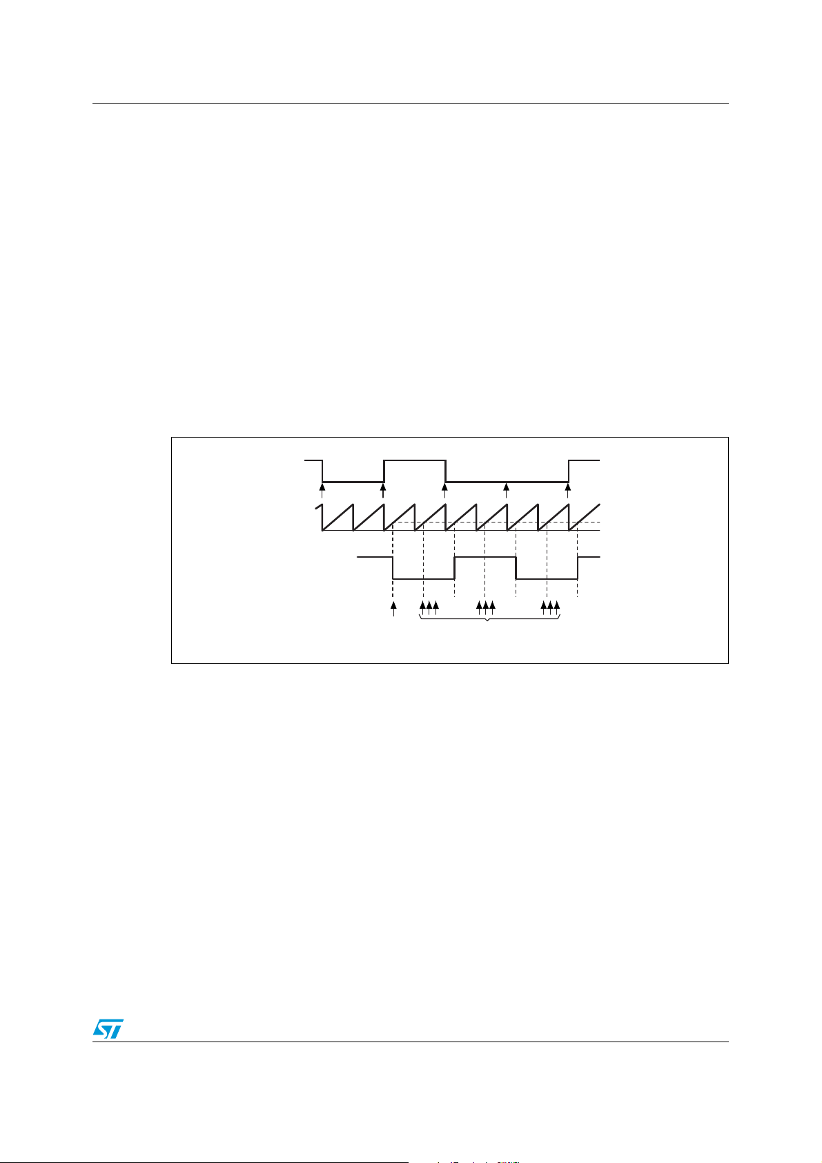
AN2781 Principle of the software solution
Tx
TCC OVF
TCC CC
Rx
Bit sampling (TCC OC)
Start bit detection
(TCC IC)
ai15179
1 Principle of the software solution
All transmit and receive processes run in the background. They are all timed by a single
CPU capture & compare timer. The associated input capture pin is dedicated to receiving
data. Any general-purpose output pin can be used for data output. The overflow period of
the timer equal to half a bit by setting the autoreload register of the timer. Figure 1 illustrates
the timing diagram.
Transmission is based on TCC overflow interrupts. After a byte is stored into the transmit
buffer, an internal transmission request appears and the nearest OVF interrupt is used to
start the current transmission. So the maximum latency for transmission start could be half a
bit. This is because the same timer is used for independent (unsynchronized) transmit and
receive processes. Every pair OVF (overflow) interrupt controls the consecutive edge
changes of the transmitted signal on the dedicated output pin until the end of the frame
transmission. Odd OVF interrupts are discarded. Any CPU pin with the output capability
could be used as a transmit pin.
Figure 1. Capture & compare timing
The receive process uses the capture and compare feature of a single timer channel and its
dedicated pin. Initially, the input capture is performed at the channel. After detecting the first
falling edge, the value captured in the TCC capture registers is then used for compare
purposes because the channel input capture functionality is switched to output compare
(without affecting the output pin of the channel since it is not enabled). Due to the half-a-bit
overflow period of the timer, the nearest output compare event must point to the middle of
the first receive bit (start bit). Three consecutive samples are performed at the input pin at
that moment and if, for each of them, a low level is detected, the correctly received start bit is
evaluated. The receive process then continues watching every next odd output compare
interrupt. The three samples are performed with noise detection logic for the other received
data bits until the end of the current receive frame. All even compare interrupts are
discarded. After the stop bits of the frame are sampled, the dedicated timer channel is
switched back to input capture mode and waits for the next frame start condition. The
detection of noise while the stop bits are being sampled always causes a frame error. If
noise is detected in the start bit, the receive process is aborted and the Rx pin switches
back to input capture mode and waits for the next falling edge capture.
Doc ID 14762 Rev 2 5/14
Page 6

User interface AN2781
2 User interface
2.1 Application interface
The user can control the communication flow via interface routines that check the flow status
flags and call some macros in special cases. All these functions are defined in the swuart.c
file.
The interface is initialized prior to use by calling the init procedure. This ensures the initial
settings of all needed hardware and software.
void uart_init(void)
In addition, after the interface initialization, the receive flow has to be enabled. This can be
done by calling the macro below:
uart_receive_enable
Also, for an immediate interrupt, and to disable the receive process, the following
complementary macro can be used whenever required:
uart_receive_disable
All transmit and receive processes are self-operated and run in the background. For this
reason, the user must make sure to call the appropriate routines at the right time. There are
two basic procedures:
void uart_Tx_timing(void)
and
void uart_Rx_timing(void)
The first one controls the transmit timing and has to be called at equidistant periods of half a
bit. Here, the TCC overflow interrupt is used with the proper prescaler and autoreload
register setting in accordance with the requested baud rate.
The second one controls the receive timing and has to be called in case either the capture
or the compare event on the input pin is generated.
The following functions can be called to control the data flow:
u8 uart_send(u8 b)
and
u8 uart_read(u8 *b)
The first function (send) tries to store a byte b into the internal transmit data buffer and
returns the TRUE code if the storage operation and the start of transmission are successful.
It returns FALSE if the byte could not be temporarily stored into the buffer. The transmit data
buffer is doubled, so that the next data byte to transmit can be written while the previous
byte transmission is still in progress.
The second function (read) copies the received byte stored in the internal receive buffer to
the address given in the parameter field, and returns a copy of the lower nibble of the
internal status register. The read operation should be done before the next data byte is
received, otherwise an overflow error is signaled. If the nine data bit format is used, the
value of the 9
Calling the uart_read() function clears all associated error flags in the status register.
th
bit is also given at status register bit 5, unless this bit is forced to zero.
6/14 Doc ID 14762 Rev 2
Page 7

AN2781 User interface
The contents of this status register can be checked anytime by calling a macro with some
predefined status masks as shown below:
test_status(u8 status mask)
Calling this macro does not affect the contents of the status register. Ta bl e 1 gives the list of
all the masks defined for the status register.
Table 1. Status register bit definition
Bit number Hexadecimal mask Mask definition
0 0x01 receive_buffer_full
1 0x02 receive_noise_error
2 0x04 receive_frame_error
3 0x08 receive_buffer_overflow
4 0x10 receive_in_progress
5 0x20 receive_9th_data_bit
6 0x40 transmit_data_reg_empty
7 0x80 transmit_in_progress
1. The same bit is used to indicate a receive parity error.
(1)
In case of the nine bit data format, the set_Tx_bit9 and clr_Tx_bit9 macros are
defined to control the transmission of the 9
prior to calling the uart_send() routine. As the internal variable keeping the value of the
th
9
bit to be transmitted is not buffered, it is necessary to toggle the transmit_in_progress
flag to check the progress of the operation. Once the previous byte has been completely
transmitted, the set_Tx_bit9 or clr_Tx_bit9 macro is called to change the bit value for
the next byte to be transmitted. The received 9
uart_read() routine.
2.2 Precompile interface
It is possible to set and configure the interface in the precompiling phase by setting a
number of parameters in the “swuart.h” header file provided in the firmware package. In this
way, the code execution time is reduced to a minimum.
The definitions of the two basic parameters (SWUART_TRANSMIT_USED and
SWUART_RECEIVE_USED) involve both main transmit and receive flows at the start of the
user definition section in the header file.
Then, the user has to define the settings of the hardware and registers that correspond to
the associated timer and IO pins. This could be done in the next part of the section. Here,
the TIM3 timer is used with PD0 as the input CC pin. PD2 is used as the output pin. Tab le 2
gives settings for different communication speeds and CPU frequencies with relative errors.
th
data bit. These macros have to be called just
th
data bit is read while calling the
Doc ID 14762 Rev 2 7/14
Page 8

User interface AN2781
Table 2. Auto reload register settings (TIM3_PSCR=0)
Nominal
speed [Bd]
TIM OVF interrupt
rate [µs]
ARR setting
(16 MHz)
Error
ARR setting
(24 MHz)
Error
57600 8.68 - - 208 0.16%
19200 26.04 417 0.08% 625 0
9600 52.08 833 0.04% 1250 0
4800 104.17 1667 0.02% 2500 0
The number of data bits may be between 1 and 9. One or two stop bits may be defined. The
MSB bit may be used as an even parity bit if the PARITY flag is defined as TRUE. The
proper data format is set by using the following variables at the end of the user setting
section: DATA_LENGTH, STOP_BITS and PARITY.
8/14 Doc ID 14762 Rev 2
Page 9

AN2781 Firmware package
3 Firmware package
A complete project is included in the firmware package. This project is designed for the ST
Visual Develop (STVD) development environment and the Cosmic compiler, and has been
tested using the STM8S/128-EVAL evaluation board. To run the project example, you must
have installed STVD (at least version 3.5.0) and the Cosmic compiler for the STM8S family.
Both tools are free for download from the STMicroelectronics and Cosmic websites. Tab le 3
gives the list of the files included in the package.
Table 3. List of the files included in the firmware package
File name File contents
main.c Example of how to handle SWUART, testing routines.
swuart.c All functions.
swuart.h All user and system definitions of SWUART.
stm8s_it.c User interrupt services
stm8_interrupt_vector.c STM8S interrupt vector table.
stm8s_gpio.c Included library peripheral file
stm8s_clk.c Included library peripheral file
stm8s_tim3.c Included library peripheral file
stm8s_gpio.h Peripheral library header file
stm8s_clk.h Peripheral library header file
stm8s_tim3.h Peripheral library header file
stm8s_config.h STM8S hardware configure header
stm8s_map.h STM8S hardware mapping header.
stm8s_type.h Common data type header.
stm8s_it.h Interrupt declaration header
stm8s_lib.h Library peripheral header files
mods0.h Memory model control header
Doc ID 14762 Rev 2 9/14
Page 10

Test environments AN2781
4 Test environments
The functionality of the interface was tested on the STM8S/128-EVAL evaluation board. The
main.c file of the included project contains a simple example of how to handle this software
UART interface in pooling mode. Tx being connected to the Rx pin, the byte transmission
and reception processes are simultaneous. Every received byte is then tested for
correctness after each transmission-reception cycle. Transmission speed is 57600 Bd. A
delay of 45 ms is inserted after each byte transmission-receive cycle. Under normal
operating conditions, the LEDs on the board should be constantly lit with no visible blinking.
The HSE system clock at maximum speed (24 MHz) is activated after initialization.
For testing purposes, the user can awake a test pin service by defining the
TEST_PIN_USED switch in the user setting section of the “swuart.h” header file, and by
selecting the suitable output pin in the file. This pin signals the sampling moment of the
receive service routine, and could be used for other user purposes.
10/14 Doc ID 14762 Rev 2
Page 11

AN2781 CPU workload
5 CPU workload
The interrupt service latency could be critical for both transmit and receive processes,
especially while using a higher communication speed. The user has to handle both
processes by interrupt services of higher priority to prevent significant service latency due to
another interrupt request service. When other interrupts with the same or higher priority are
used while receiving or transmitting, the user has to make sure that these interrupts –
chained in the worst case – would not postpone the transmit and receive services by more
than 10% of the bit rate.
Ta bl e 4 and Tab le 5 give indicative values concerning CPU usage and latency time for other
interrupts. In Ta bl e 4 the communication speed is 57.6 kBd for the CPU running at the
24 MHz HSE (high-speed external) frequency, whereas in Ta b le 5 the communication speed
is 19.2 KBd for the CPU running at the maximum HSI (high-speed internal) frequency of
16 MHz. The CPU usage depends on whether the transmit or receive process is active, the
worst case being when transmit and receive processes take place simultaneously. Then the
two percentages of CPU usage must be added up. The latency time is the maximum time
the CPU spends servicing interrupts during transmit or receive.
When the line is idle, the load is lower on the transmit side but transmission services are still
called at a rate of half a bit to check for the presence of byte transmit requests. So CPU
usage can be saved by simply disabling the corresponding interrupt when no transmission is
needed. The CPU load can also be reduced by 1/3, approximately, on the transmit side if
two separate timers are used to control the transmit and receive processes independently.
Then every bit can be controlled by one interrupt service only instead of the two currently
used. CPU usage on the receive side is zero when the line is idle because the process waits
for the interrupt generated by the falling edge of the start bit.
Table 4. CPU usage and maximum latency times for a speed of 57.6 KBd when the
core runs at the maximum HSE frequency
57600 Bd
24 MHz
Transmit ~25% 3 µs ~15% 2 µs
Receive ~35% 5 µs 0% 0 µs
Table 5. CPU usage and maximum latency times for a speed of 19.2 KBd when the
Data byte on Rx / Tx pin Idle on Rx / Tx pin
CPU usage Latency (max) CPU usage Latency (max)
core runs at the maximum HSI frequency
19200 Bd
16 MHz
Transmit ~12% 5 µs ~7% 4 µs
Receive ~17% 9 µs 0% 0 µs
Data byte on Rx / Tx pin Idle on Rx / Tx pin
CPU usage Latency (max) CPU usage Latency (max)
Doc ID 14762 Rev 2 11/14
Page 12

Other solutions AN2781
6 Other solutions
In this application note, emulation is implemented using the Rx pin with the input capture
capability. For lower speeds, however, any other pin with the interrupt capability can be used
as the Rx pin. If the second solution is adopted, the user then has to copy the contents of
the timer registers to the compare registers on the falling edge of the incoming start bit. The
user should also enable or disable the interrupts depending on whether a receive operation
is in progress.
Even though the code is executed and tested for the STM8S core, any other device with
similar capture and compare capability may be used. It is possible to use two separate
timers to control the receive and transmit processes independently, too. It is especially
useful when different speeds are used for transmission and reception, when immediate
transmission start with no delay is critical, or in case the CPU usage should be decreased.
12/14 Doc ID 14762 Rev 2
Page 13

AN2781 Revision history
7 Revision history
Table 6. Document revision history
Date Revision Changes
12-Sep-2008 1 Initial release.
25-Aug-2011 2 Updated to refer to STM8S and STM8A products
Doc ID 14762 Rev 2 13/14
Page 14

AN2781
Please Read Carefully:
Information in this document is provided solely in connection with ST products. STMicroelectronics NV and its subsidiaries (“ST”) reserve the
right to make changes, corrections, modifications or improvements, to this document, and the products and services described herein at any
time, without notice.
All ST products are sold pursuant to ST’s terms and conditions of sale.
Purchasers are solely responsible for the choice, selection and use of the ST products and services described herein, and ST assumes no
liability whatsoever relating to the choice, selection or use of the ST products and services described herein.
No license, express or implied, by estoppel or otherwise, to any intellectual property rights is granted under this document. If any part of this
document refers to any third party products or services it shall not be deemed a license grant by ST for the use of such third party products
or services, or any intellectual property contained therein or considered as a warranty covering the use in any manner whatsoever of such
third party products or services or any intellectual property contained therein.
UNLESS OTHERWISE SET FORTH IN ST’S TERMS AND CONDITIONS OF SALE ST DISCLAIMS ANY EXPRESS OR IMPLIED
WARRANTY WITH RESPECT TO THE USE AND/OR SALE OF ST PRODUCTS INCLUDING WITHOUT LIMITATION IMPLIED
WARRANTIES OF MERCHANTABILITY, FITNESS FOR A PARTICULAR PURPOSE (AND THEIR EQUIVALENTS UNDER THE LAWS
OF ANY JURISDICTION), OR INFRINGEMENT OF ANY PATENT, COPYRIGHT OR OTHER INTELLECTUAL PROPERTY RIGHT.
UNLESS EXPRESSLY APPROVED IN WRITING BY TWO AUTHORIZED ST REPRESENTATIVES, ST PRODUCTS ARE NOT
RECOMMENDED, AUTHORIZED OR WARRANTED FOR USE IN MILITARY, AIR CRAFT, SPACE, LIFE SAVING, OR LIFE SUSTAINING
APPLICATIONS, NOR IN PRODUCTS OR SYSTEMS WHERE FAILURE OR MALFUNCTION MAY RESULT IN PERSONAL INJURY,
DEATH, OR SEVERE PROPERTY OR ENVIRONMENTAL DAMAGE. ST PRODUCTS WHICH ARE NOT SPECIFIED AS "AUTOMOTIVE
GRADE" MAY ONLY BE USED IN AUTOMOTIVE APPLICATIONS AT USER’S OWN RISK.
Resale of ST products with provisions different from the statements and/or technical features set forth in this document shall immediately void
any warranty granted by ST for the ST product or service described herein and shall not create or extend in any manner whatsoever, any
liability of ST.
ST and the ST logo are trademarks or registered trademarks of ST in various countries.
Information in this document supersedes and replaces all information previously supplied.
The ST logo is a registered trademark of STMicroelectronics. All other names are the property of their respective owners.
© 2011 STMicroelectronics - All rights reserved
STMicroelectronics group of companies
Australia - Belgium - Brazil - Canada - China - Czech Republic - Finland - France - Germany - Hong Kong - India - Israel - Italy - Japan -
Malaysia - Malta - Morocco - Philippines - Singapore - Spain - Sweden - Switzerland - United Kingdom - United States of America
www.st.com
14/14 Doc ID 14762 Rev 2
 Loading...